Corresponding author: S. Burger
URL: http://www.zib.de/en/numerik/computational-nano-optics.html
URL: http://www.jcmwave.com
Email: burger@zib.de
3D finite element simulation of optical modes in VCSELs
Abstract
We present a finite element method (FEM) solver for computation of optical resonance modes in VCSELs. We perform a convergence study and demonstrate that high accuracies for 3D setups can be attained on standard computers. We also demonstrate simulations of thermo-optical effects in VCSELs.
keywords:
3D VCSEL simulation, optical mode solver, thermal lensing effect, finite element methodThis paper will be published in Proc. SPIE Vol. 8255 (2012) 82550K (Physics and Simulation of Optoelectronic Devices XX; Bernd Witzigmann, Marek Osinski, Fritz Henneberger, Yasuhiko Arakawa, Editors, DOI: 10.1117/12.906372), and is made available as an electronic preprint with permission of SPIE. One print or electronic copy may be made for personal use only. Systematic or multiple reproduction, distribution to multiple locations via electronic or other means, duplication of any material in this paper for a fee or for commercial purposes, or modification of the content of the paper are prohibited.
1 Introduction
Vertical-cavity surface-emitting lasers (VCSELs) are light sources with unique properties and potential applications of great interest [1]. Solution of Maxwell’s equations for realistic 3D VCSELs is a challenging task [2]. Since the VCSEL resonator is realized by distributed Bragg reflectors (DBR), the geometry inherits a pronounced multiscale structure. The devices are relatively large (thousands of cubic wavelengths) and contain subwavelength DBR layers, very thin active zones and structured apertures. Further, the infinite exterior adjacent to the VCSEL containing also a layered structure has to be modeled to obtain realistic predictions of radiation loss and lasing threshold. A variety of methods has been used to compute optical VCSEL modes. These include FEM, finite difference time-domain methods (FDTD), modal expansion and approximative methods [3, 4, 2, 5]. In most standard approaches the optical problem is restricted to purely 1D or to cylindrically symmetric structures. Nevertheless, many realistic 3D devices cannot be restricted in this way. This is the reason why reliable full 3D simulations become so important. Accuracy limitations of state-of-the-art 3D solvers, including also FEM solvers, have recently been discussed [2, 5].
The finite element method is very well suited for simulation of nano-optical systems and devices [6, 7]. Its main features are the capability of exact geometric modeling due to usage of unstructured meshes and high accuracy at low computational cost. The finite element method offers great flexibility to approximate the solution: different mesh sizes and polynomial ansatz functions of varying degree can be combined to obtain high convergence rates. As a result, very demanding problems can be solved on standard workstations [8]. We demonstrate that a FEM eigenmode solver with higher-order finite elements, adaptive meshing and a rigorous implementation of transparent boundary conditions is a powerful method for 3D VCSEL mode computation.
2 Mathematical Background
The main physical effects in a VCSEL are associated to time scales ranging over several orders of magnitude. Since the frequency of the optical modes is much higher than those of all other effects, a time-harmonic ansatz for the electric field is well-justified:
| (1) |
where denotes the frequency. Using this ansatz in Maxwell’s equations, the following second order equation for the electric field can be derived:
| (2) |
In this equation no exterior current or charge density sources are present. Physically, the light field of a VCSEL is created by coupling of the electron system in the active layer to the eigenmodes of the structure. In Maxwell’s equations this usually enters via the complex permittivity tensor (in all relevant optical materials the magnetic permeability is a constant). The resonance problem then consists of finding pairs , such that Maxwell’s equations (2) on the given geometry are fulfilled. Furthermore, the so called radiation condition has to be satisfied which requires that the resonance modes are purely outward radiating. For solving equations (2) we use the FEM package JCMsuite developed by ZIB and JCMwave [6].

3 VCSEL model and simulation results
The aim of this paper is to demonstrate that very low numerical errors can be reached in full 3D VCSEL simulation. In order to quantify the error of a numerical solution we compare it to a reference solution. Because for the full 3D VCSEL problem no accurate quantitative results are available as independent reference, we use a cylindrically symmetric VCSEL setup in this convergence study. A very accurate solution to this problem can be obtained using a 2D solver in cylindrical coordinates [7]. Restriction of 3D resonance mode computations to a 2D cross section due to the cylindrical symmetry leads to substantial savings in computational time and memory requirements. The 3D, rotationally symmetric solution can also be compared to results from the literature [3]. With the reference solution at hand we perform simulation of the same physical setup using a full 3D FEM model. Numerical accuracy of the 3D results from this model is then obtained from comparison to the reference solution.
In a further sub-section, we demonstrate 3D simulation of the thermal lensing effect in a VCSEL.
3.1 2D reference solution
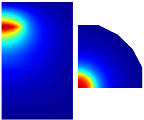
As physical model we choose a VCSEL setup as described by Bienstman et al. [3]. The laser consists of two DBR mirrors with alternating AlGaAs-GaAs layers. The InGaAs quantum well layer (gain material) is embedded in the central GaAs cavity region. An AlOx aperture is placed in the upper region of the lowest AlGaAs layer of the top mirror. The whole structure is situated on a GaAs substrate. Figure 1a shows a 2D cross section through the cylindrically symmetric setup. Note that the layered structure extends infinitely in radial direction and modal confinement is reached through the finite AlOx aperture and the finite active region.
We use a 2D FEM solver in cylindrical coordinates to obtain the near field solution and the complex eigenfrequency . From we derive the resonance wavelength , where denotes the speed of light, and the damping factor , which quantifies the gain/loss of the cavity mode. Figure 1b shows the electric field intensity distribution of the fundamental VCSEL mode in a pseudo-color representation.
We have computed solutions to the same physical setup using different numerical resolutions, where we have varied finite element degree and the mesh refinement. With increasing and increasing mesh refinement also the number of unknowns of the FEM problem, , increases. Using the solution with highest and highest refinement (, 4 successive adaptive grid refinements) as reference we can attribute relative numerical errors to the computed resonance wavelengths and damping factors. Figure 2 shows how these converge with increasing . We have also checked convergence with respect to the numerical parameters of the perfectly matched layers (PML) [6]. We observe that very high accuracies can be reached with relative errors below for the resonance wavelength. Note that the relative error of the damping factor is larger due the much smaller total value of the imaginary part of the fundamental eigenvalue. However, also here we reach relative accuracies below 0.001%.
3.2 Full 3D computation
For full 3D computation of the same VCSEL setup as before we discretize the VCSEL geometry using a 3D prismatoidal mesh. Figure 3 (left) shows a visualization of the mesh discretizing the geometry. Note that due to mirror symmetries of the device we can restrict the computational domain to one quarter of the full VCSEL, on the mirror faces boundary conditions corresponding to the symmetry of the fundamental mode are applied. Further, transparent boundary conditions, realized with perfectly matched layers are applied. Figure 3 (right) shows a cross section through the computed 3D field distribution (). As expected the field distribution agrees perfectly with the field distribution of the reference solution and the resonance wavelengths agree to high precision.
Again we perform a convergence study where we vary finite element degree . The relative errors are defined as deviations from the 2D cylindrically symmetric reference solution (see above), normalized to the reference solution result. Figure 4 shows that we reach an accuracy of the resonance wavelength well below and an accuracy of the damping factor below . Computational times for the full 3D simulations are few minutes on a standard workstation (3 min (), 6 min (), resp. 30 min ()).
In the previous we have simulated a ”cold cavity” VCSEL, i.e., without gain in the active zone. Next we demonstrate the accuracy of laser threshold computation. For this we perform computations with increasing gain in the active zone (imaginary part of the complex refraction index of the quantum well layer, ). Figure 4b shows the expected linear dependence of the damping factor on material gain . We observe that threshold is reached at a refractive index . This value is obtained from 3D simulation at both investigated accuracy levels, as well as from the 2D cylindrically symmetric reference simulation. The agreement corresponds to the accuracy of the damping factor better than 1% relative deviation as displayed in Fig. 4.
Now, that we have characterized the accuracy level which can be reached by the 3D FEM solver for typical VCSEL setups we turn to a “real”, i.e., non-rotationally-symmetric VCSEL geometry. Figure 5 shows a visualization of the mesh and the fundamental mode of a photonic-crystal VCSEL in a setup as described in [2]. We have used simulation accuracy settings as in the previous results. We therefore expect that the numerical accuracy of the wavelength is of the order of and the numerical accuracy of the damping factor is of the order of , c.f., Fig. 4. This is a significantly higher accuracy than reached in the benchmark of Dems et al. [2]. A main difference in our implementation, compared to the FEM implementation in Dems et al. [2], is the usage of higher-order elements, and of adaptive transparent boundary conditions [6].
3.3 Thermo-optical simulations
Limitations of the output profile quality of VCSELs can be due to unconverted pump power in the active region which leads to a local heating and through thermo-optical coupling to inferior laser mode properties. In this subsection we present 3D thermo-optical simulations based on the stationary heat conduction equation
where denotes the thermal conductivity, denotes the temperature and is the thermal source density. We couple this equation to the optical simulation via the thermo-optical correction of the temperature dependent relative permittivity , where is the thermo-optical coefficient and is a reference temperature.
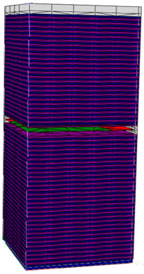
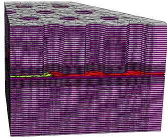
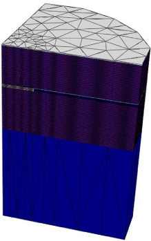
We investigate the same VCSEL geometry and material parameters as in the previous Section 3.2. For the thermal simulation we need to expand the computational domain (GaAs substrate) in order to set suitable boundary conditions, i.e., to fix the boundary temperature of the computational domain, , at K. We define a heat source in the oxide aperture and in the cavity by setting the thermal source density in the according regions and compute the temperature distribution within the VCSEL by solving the stationary heat equation. Fig. 6 shows visualizations of the discretized geometry and of a computed temperature distribution. We then use this temperature distribution to define a locally varying permittivity correction throughout the VCSEL geometry, and compute the optical cavity modes using the Maxwell solver as in Section 3.2.
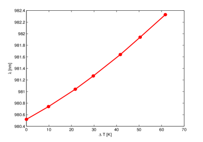
We have performed simulations for various heat source powers: Figure 7 shows the almost linear dependence of the resonance wavelength on the maximum temperature difference in the device. Increasing the maximum temperature in the device through increasing heat source power causes a refractive index change of the DBR structure and a shift of its reflective wavelength. Thus the VCSEL resonance wavelength is shifted.
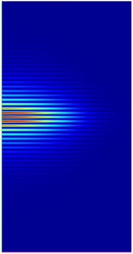
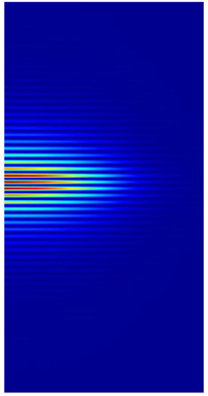
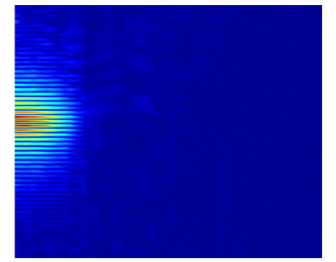
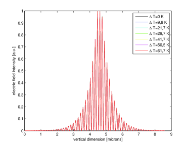
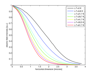
In post-processes, from the near field distribution we exported 1D electric field intensity distributions () in both, vertical and horizontal directions, through the cavity center. The electric field along the vertical dimension is nearly independent on temperature variations, as expected, see Fig. 8a. In the horizontal direction we observe the constriction of the electric field intensity with increasing temperature, see Fig. 8b. Such behaviour is known as thermal lensing effect and a limitation for high-power semiconductor lasers. In specific applications, VCSELs should be designed for low thermal lensing [9].
4 Conclusion
We have presented FEM results for resonance mode computation in VCSELs. Our results for a cylindrically symmetric device demonstrate fast convergence and high accuracy of the method. The resonance wavelength and the corresponding damping factor can be computed very accurately with relative errors below , respectively . The reached accuracies are several orders of magnitude higher than the differences between the results from different models presented in Ref. [3].
Comparison of full 3D simulation results to the 2D solution and a detailed convergence analysis confirm the high accuracy of the method also for full 3D problems with relative errors of the wavelength and the corresponding damping factor below , respectively . To our knowledge results on numerical accuracy of 3D VCSEL simulations on this level have not previously been published (see, e.g., [3, 4, 2]). We have also presented thermo-optical simulations for 3D VCSELs. In future research we plan to investigate more complex 3D device geometries like metal cavity surface-emitting microlasers.
Acknowledgments
We acknowledge funding by the Deutsche Forschungsgemeinschaft (DFG, German Research Foundation) within SFB 787 Halbleiter Nanophotonik.
References
- [1] Iga, K., “Surface-emitting laser - its birth and generation of new optoelectronics field,” IEEE Journal on Selected Topics in Quantum Electronics 6, 1201–1215 (2000).
- [2] Dems, M., Chung, I.-S., Nyakas, P., Bischoff, S., and Panajotov, K., “Numerical methods for modeling photonic-crystal VCSELs,” Optics Express 18, 16042–16054 (2010).
- [3] Bienstman, P., Baets, R., Vukusic, J., Larsson, A., Noble, M. J., Brunner, M., Gulden, K., Debernardi, P., Fratta, L., Bava, G. P., Wenzel, H., Klein, B., Conradi, O., Pregla, R., Riyopoulos, S. A., Seurin, J.-F. P., and Chuang, S. L., “Comparison of optical VCSEL models on the simulation of oxide-confined devices,” IEEE Journal of Quantum Electronics 37, 1618–1631 (2001).
- [4] Nyakas, P., “Full-vectorial three-dimensional finite element optical simulation of vertical-cavity surface-emitting lasers,” Journal of Lightwave Technology 25, 2427–2434 (2007).
- [5] Liu, F., Xu, C., Xie, Y.-Y., Zhao, Z.-B., Zhou, K., Wang, B.-Q., Liu, Y.-M., and Shen, G.-D., “Full 3D FDTD analysis of electromagnetic field in photonic crystal VCSEL,” 3rd International Photonics&Optoelectronics Meetings(POEM2010) 276, 012071 (2011).
- [6] Pomplun, J., Burger, S., Zschiedrich, L., and Schmidt, F., “Adaptive finite element method for simulation of optical nano structures,” phys. stat. sol. (b) 244, 3419–3434 (2007).
- [7] Karl, M., Kettner, B., Burger, S., Schmidt, F., Kalt, H., and Hetterich, M., “Dependencies of micro-pillar cavity quality factors calculated with finite element methods,” Optics Express 17, 1144–1158 (2009).
- [8] Burger, S., Zschiedrich, L., and Schmidt, F., “Numerical investigation of optical resonances in circular grating resonators,” Silicon Photonics V 7606, 760610 (2010).
- [9] Wenzel, H., Crump, P., Ekhteraei, H., Schultz, C., Pomplun, J., Burger, S., Zschiedrich, L., Schmidt, F., and Erbert, G., “Theoretical and experimental analysis of the lateral modes of high-power broad-area lasers,” in [11th International Conference on Numerical Simulation of Optoelectronic Devices (NUSOD) ], 143–144 (2011).