Ink-Jet Printed Graphene Electronics
Abstract
We demonstrate ink-jet printing as a viable method for large area fabrication of graphene devices. We produce a graphene-based ink by liquid phase exfoliation of graphite in N-Methylpyrrolidone. We use it to print thin-film transistors, with mobilities up to95cm2V-1s-1, as well as transparent and conductive patterns, with80 transmittance and30k/ sheet resistance. This paves the way to all-printed, flexible and transparent graphene devices on arbitrary substrates.
I Introduction
Flexible electronics is a rapidly expanding research areaCao2008 . Applications include touch screensZhou2006 , electronic paper (e-paper)Ota1973 ; Gelinck2004 , sensorsSekitani2009 , radio frequency tagsMyny2009 , photovoltaic cellsGranqvist2007 ; Yoon2008 , and electronic textilesSchmied2009 . To date, it mainly relies on two fabrication strategies: one in which substrates bearing thousands of Field-effect Transistors (FETs) are bonded to plastic by transfer printing or pick-and place methodskim2008 ; another in which FETs are prepared directly on the target substrate by several coating, curing and lithographic stepsSingh2006 ; Cao2008 . Rubber stampingRogers2001 , embossingForrest2004 and ink-jet printingBao1999 ; Sirringhaus2000 reduce the number of such fabrication steps.
Ink-jet printing is one of the most promising techniques for large area fabrication of flexible plastic electronicsSirringhaus2000 . A range of components can be printed, such as transistorsForrest2004 ; Sirringhaus2000 ; Sun2006 ; McAlpine2005 ; Singh2010 , photovoltaic devicesPeumans2003 , organic light emitting diodes (OLEDs)Forrest2004 ; Servati2005 ; Singh2010 , and displaysForrest2004 . Ink-jet printing is versatileSingh2010 , involves a limited number of process stepsdeGans2004 , is amenable for mass production, and can deposit controlled amounts of materialdeGans2004 . Drop on demanddeGans2004 ; Dong2006 ink-jet printing has progressed from printing text and graphicsdeGans2004 , to a tool for rapid manufacturingvan Osch2008 , being now an established technique to print Thin Film Transistor (TFT) based on organic conducting and semiconducting inksSirringhaus2000 ; Sekitani2009 ; Yoo2010 . However, their mobilities, 0.5cm2V-1s-1,Sekitani2009 ; Singh2010 are still much lower than standard silicon technology. Several approaches aim to improve this, such as the use of polysiliconShimoda2006 , zinc oxide nanoparticlesNoh2007 and carbon nanotubes (CNTs)Beecher2007 ; Hsieh2009 ; Takenobu2009 ; Okimoto2009 ; Okimoto2010 ; Ha2010 . Metal nanoparticle inks are not stable in ordinary solvents, such as Deionized (DI) Water, Acetone, Isopropyl Alcohol, N-Methylpyrrolidone (NMP), TetrahydrofuranSingh2010 ; Luechinger2008 . They need to be chemically modified in order to be dispersedSingh2010 , using stabilizers, which usually degrade in a couple of yearsSingh2010 ; Luechinger2008 . Metal nanoparticles also tend to oxidize after printingSingh2010 ; Luechinger2008 . Ink-jet printed CNT-TFTs have been reported with up to 50cm2 V-1s-1 and a ON/OFF ratio103.Ha2010
Graphene is the two-dimensional (2d) building block for carbon allotropes of every other dimensionality. It can be stacked into 3d graphite, rolled into 1d nanotubes, or wrapped into 0d fullerenesGeim_rise2007 . It is at the centre of an ever expanding research areaGeim_rise2007 ; Novoselov2004 ; Charlier2008 ; Bonaccorso2010 . Near-ballistic transport and high mobility make it an ideal material for nanoelectronics, especially for high frequency applicationsLin2010 . Furthermore, its optical and mechanical properties are ideal for micro and nanomechanical systems, thin-film transistors, transparent and conductive composites and electrodes, and photonicsGeim_rise2007 ; Bonaccorso2010 ; sunacsnano10 . Graphene was isolated by micromechanical exfoliation of graphiteNovoselovPNAS2005 . This technique is still the best in terms of purity, defects, mobility and optoelectronics properties. However, large scale production approaches are needed for widespread application. These encompass growth by chemical vapor deposition (CVD)Karu1966 ; Obraztsov2007 ; Kim2009 ; Reina2009 ; Li2009 ; Bae2010 , segregation by heat treatment of silicon carbideBerger2006 ; Acheson1896 ; Badami1962 ; Emtsev2009 and metal substratesOshima1997 ; Gamo1997 ; Rosei1983 ; Sutter2008 , liquid phase exfoliation (LPE)Hernandez2008 ; Lotya2009 ; Valles2008 ; Hasan2010 . Amongst these, LPE is ideally suited to produce printable inks.
Graphite can be exfoliated by chemical wet dispersion followed by ultrasonication, both in aqueousLotya2009 ; Hasan2010 and non-aqueous solventsHernandez2008 ; Hasan2010 . Dispersions can be achieved by mild sonication in water with Sodium Deoxycholate, followed by sedimentation based-ultracentrifugationHasan2010 ; Marago2010 . Bile salt surfactants also allow the isolation of flakes with controlled thickness, when combined with density gradient ultracentrifugation (DGU)Greennlett2009 . Exfoliation of graphite intercalated compoundsValles2008 and expandable graphiteLiScience2008 was also reported.
LPE was first achieved through sonication of graphite oxideStankovich2006 , following the Hummers methodHummers1958 . The oxidation of graphite in the presence of acids and oxidantsBrodie1860 ; Staudenmaier1898 disrupts the sp2-network and introduces hydroxyl or epoxide groupsMattevi2009 ; Cai2008 , with carboxylic or carbonyl groups attached to the edgeMattevi2009 ; Cai2008 . These make graphene oxide (GO) sheets readily dispersible in waterEda2010 ; Stankovich2006 and several other solventsGO_organic_08 . Although large GO flakes can be produced, these are intrinsically defectiveStankovich2006 ; he_GO_model_98 , and electrically insulatingStankovich2006 ; Mattevi2009 . Despite several attemptsStankovich2006 ; Mattevi2009 , reduced GO (RGO) does not fully regain the pristine graphene electrical conductivityEda2008 ; Mattevi2009 . It is thus important to distinguish between dispersion processed graphene flakesHernandez2008 ; Lotya2009 ; Valles2008 ; Hasan2010 , retaining the electronic properties of graphene, and insulating GO dispersionsStankovich2006 ; Eda2008 . Several groups reported GO-based inksDua2010 ; Wang2009 ; Luechinger2008 . Ref. Dua2010, ink-jet printed RGO films for sensors applications, while Ref. Luechinger2008, produced RGO-stabilized Cu nanoparticles as low temperature metal colloids, to replace standard metal nanoparticle inks, that require high temperature sintering postprocessingPark2007 . Mobilities up to 90cm2V-1s-1 have been achieved for highly reduced GO films by ink-jet printingWang2009 , with an ON/OFF ratio up to 10.Wang2009
Here we produce a graphene-based ink and demonstrate its viability for printed electronics.
II Results and discussion
III Ink requirements
A key property of inks viable for printing is their ability to generate dropletsReis2000 ; Jang2009 . Ink viscosity, [mPa s], surface tension, [mJ m-2], density, [g cm-3], and nozzle diameter, [m], influence the spreading of the liquid dropsFromm1984 ; Reis2000 ; Jang2009 . These parameters can be arranged into dimensionless figures of merit (FOM), such as the Reynolds (Re)Fromm1984 ; Reis2000 ; Jang2009 , Weber (We)Fromm1984 ; Reis2000 ; Jang2009 , and Ohnesorge (Oh)Fromm1984 ; Reis2000 ; Jang2009 numbers: Re=; We=, Oh=, where [m/s] is the drop velocity.
Refs. Fromm1984, ; Reis2000, ; Jang2009, suggested to use Z=1/Oh as the appropriate FOM to characterize drop formation, 1Z14 being required to get stable drop generationReis2000 ; Jang2009 . For Z1 the high viscosity prevents drop ejectionReis2000 ; Jang2009 , whereas at Z14 the primary drop is accompanied by a number of satellite dropletsReis2000 ; Jang2009 . Moreover, when inks contain dispersed molecules or nano-particles, the latter should be smaller than the nozzle diameter, to prevent cloggingvan Osch2008 ; deGans2004 . Refs. van Osch2008, ; Microfab1999, suggested that the size of such molecules or particles should be at least 1/50 of the nozzle diameter, in order to exclude any printing instability, such as clustering of the particles at the nozzle edge, which may deviate the drop trajectory, or result in agglomerates that will eventually block the nozzle.
The ejected drop behavior on the substrate can be efficiently described by fluid dynamics. When a small liquid droplet is in contact with a flat surface, partial wetting results in a finite angle between the liquid and the substratedeGennes1985 , known as contact angle, Shafrin1960 ; deGennes1985 ; Israelachvili1991 . The lower drop size limit is given byReis2000 ; Jang2009 . Thus, e.g., for a typical =50m, =20, =58 and 45∘, we get 85-90m. The distance from the substrate must be optimized to guarantee both homogeneous printing and the highest resolution, barring any unusual jetting conditions, such as perturbations from the surrounding environment and diversion of the drop trajectoryReis2000 ; Derby2003 ; Singh2010 . Furthermore, a substrate very close to the nozzle causes secondary drops to scatter off during the impact of the primary dropSingh2010 ; Park2010 , due to the initial drop jetting pressure, thus affecting the homogeneity of the final printed featuresPark2010 . The final assembly of printed nano-particle inks depends on the substrate Surface Energy (SE)deGans2004 ; van Osch2008 , as well as the ink viscosity and surface tensiondeGans2004 .
When a drop of an ink containing dispersed particles evaporates on a surface it commonly leaves a dense, ring-like, deposit along its perimeterdeGans2004 ; van Osch2008 . This is the so-called ”coffee ring effect”Deegan1997 , i.e. a distortion of the drops during solvent drying due to the interplay of ink viscosity and solute transport via solvent motion (arising from surface tension interaction between solvent and substrate)Deegan1997 ; Singh2010 . This is one of the most important phenomena affecting the homogeneity of ink-jet printed dropsDeegan1997 ; Singh2010 . In order to prevent this, it is necessary to ”freeze” the drops geometry immediately after they form an homogeneous and continuous film on the substrateSingh2010 .
Here we use an ink-jet printer with a nozzle diameter50m, thus we need to have flakes less than 1m across. By tuning , and we will target a Z within the optimal range. We print on Si/SiO2 (to probe the electrical properties of the ink) and borosilicate (Pyrex 7740-Polished Prime Grade) glass substrates (to test the ink as transparent conductor), both with a roughness Rz15nm. Our aim is to obtain ink-jet printed drops on the substrate, with homogeneous flakes and uniform morphology, i.e. with roughness comparable to the substrate. We obtain this by varying the contact angle and optimizing the substrate wettability.
In order to reduce the coffee ring effect we need both a solvent with boiling point (Tc [∘C]) and heat of vaporization (Vc [kJ/mol]) higher than waterDeegan1997 ; Derby2003 ; Singh2010 , and a substrate that promotes adhesionOsthoff2007 . Thus, we use NMP as solvent for two main reasons. First, it has higher boiling point (202∘C)HandchemLide and heat of vaporization (54.5kJ/mol)HandchemLide , than water (100∘C and 40kJ/mol). Second, NMP is the best solvent to get high-yield, surfactant-free exfoliation of graphiteHernandez2008 ; Hasan2010 . We then test several surface treatments to optimize substrate adhesion. After printing, NMP is removed by thermal annealing at 170∘C for 5 minutes.
III.1 Graphene-based printable ink
We prepare the graphene-based printable ink as follows. Graphite flakes (NGS Naturgraphit) are sonicated (Decon bath, 100W) in NMP for 9 hours. The un-exfoliated flakes are left to settle for 10 mins after sonication. The decanted dispersions are then ultracentrifuged using a TH-641 swinging bucket rotor in a Sorvall WX-100 Ultra-centrifuge at 10,000 rpm (15,000g) for an hour and filtered to remove flakes1m, that might clog the nozzle. The resulting ink is characterized by Optical Absorption Spectroscopy (OAS), High Resolution Transmission Electron Microscopy (HRTEM), Electron diffraction and Raman spectroscopy.
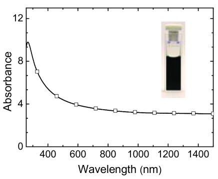
A Perkin-Elmer Lambda 950 spectrometer with 1nm resolution is used for OAS measurements. OAS can be used to estimate the concentration of grapheneHernandez2008 ; Lotya2009 ; Marago2010 using the Beer-Lambert Law according to the relation , where A is the absorbance, l [m] is the light path length, c [g/L] the concentration of dispersed graphitic material and [L g-1 m-1] the absorption coefficient. Fig.1 plots an OAS spectrum of our ink diluted to 10%. The ink is diluted to avoid strong scattering losses at higher concentrations, which could cause deviation of the measured value of A from the Beer-Lambert law. The spectrum in Fig.1 is mostly featureless, as expected due to the linear dispersion of the Dirac electronssunacsnano10 ; makprl08 ; kravetsprb10 ; Bonaccorso2010 ; Nair2008 ; Casiraghi2007 , the peak in the UV region being a signature of the van Hove singularity in the graphene density of stateskravetsprb10 . From 1390Lg-1m-1 at 660nm, as for Refs. Lotya2009, ; Hasan2010, , we estimate c0.110.02g/L.
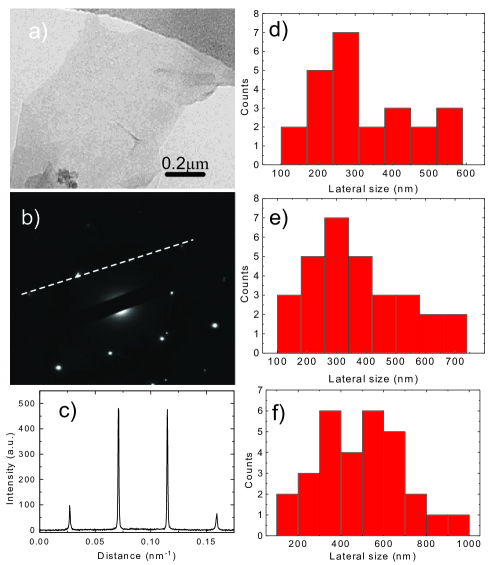
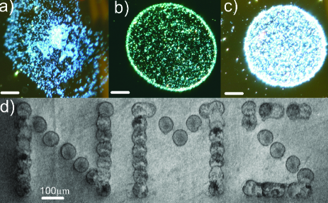
We disperse drops of our ink on Holey carbon Transmission electron microscopy (TEM) grids for analysis using a Tecnai T20 high resolution TEM, with an acceleration voltage of 200KV operating in phase contrast mode. Fig.2a is HRTEM image of a Single Layer Graphene (SLG) flake from the ink, while Fig.2b is a normal-incidence electron diffraction of the same flake of Fig.2a. It shows the expected sixfold symmetryMeyer_nature2007 ; Meyer_SSC2007 ; Ferrari2006 . The peaks are labeled with the corresponding Miller-Bravais (hkil) indexes. For Few Layer Gaphene (FLG) flakes with Bernal (AB) stacking, the intensity ratio is1, while for SLG 1Meyer_nature2007 ; Ferrari2006 . We use this to distinguish SLG from FLGsHernandez2008 ; Marago2010 . Fig.2c plots the diffraction intensity measured along the line section through the (110), (010), (010), (110) axis, reported in Fig.2b. The inner peaks, (010) and (010), are1.5 times the outer ones, (110) and (110), indicating that the flake is SLGMeyer_nature2007 . The analysis of the edges also gives a reliable information on the number of layers and can be used to investigate a large number of flakesMeyer_nature2007 , from zoomed-in high resolution edge imagesHernandez2008 ; Khan2010 . If SLG folds or several SLGs stack one on the other, selected area diffraction is used to distinguish contentious cases.
These combined analysis show that our ink mostly consists of SLGs, Bi-Layers (BLG) and FLGs, with lateral size300-1000nm. We find that35% SLGs are larger than 300nm (Fig.2d);40% BLGs are larger than 350nm (Fig.2e);55% FLGs are larger than 450nm (Fig.2f). In particular, we have33% SLG with c0.11g/L. Previous works on LPE of graphite in NMP reported up to28% SLG for c0.18g/LHasan2010 and 21% for c1.8g/LKhan2010 . Ref. Valles2008, also reported exfoliation of intercalated graphite in NMP, with20% SLGs for c0.01g/L. Thus, our ink has higher SLG yield with respect to previous works, but lower c than Ref.Khan2010, . This higher c was achieved by long time (up to 460h) ultrasonicationKhan2010 . However Ref. Khan2010, reported defects and reduction of size as a result. Our combination of low-power sonication (25W) and ultracentrifugation is ideal for high-yield of defect-free SLGs.
Stable dispersions require the Gibbs free energy of mixing, , to be zero or negativehansenbook , where , K being the temperature, the enthalpy of mixing and and the entropy change in the mixing processHernandez2008 ; hansenbook . For graphene and nanotubes, is smallHernandez2008 ; Bergin2008 . Therefore, for dispersion and stabilization of graphene in solvents, needs to be very small. This can be achieved by choosing a solvent whose surface energy is very close to that of grapheneHernandez2008 . The surface energy of NMP satisfies this requirement and allows efficient exfoliation of graphite. Graphite can also be efficiently exfoliated in water with the use of bile salt surfactants. Ref. Lotya2010, reported20%SLGs and c0.3g/L SLGs, while Ref. Marago2010, reported60% SLGs for c0.012g/L. The yield can be increased up to80% by density gradient ultracentrifugationGreennlett2009 . The flake size of LPE graphene in water-surfactant dispersions is on average smaller(200nmLotya2010 , 30nmMarago2010 ) than thus far reported for NMP(1mHasan2010 ; Hernandez2008 ). The viscosity at room temperature of NMP (1.7mPasHandchemLide ) is higher than water (1mPasHandchemLide ). Larger flakes in a higher viscosity medium (such as NMP) experience higher frictional forceWilliams1958 ; Schuck2000 and sedimentation coefficientSvedberg1940 ; Schuck2000 , making it more difficult for them to sediment during ultracentrifugation. This reduces the SLG yield in NMP compared to water.
The centrifuged dispersions are drop-cast onto a Si wafer with 300nm thermally grown SiO2 (LDB Technologies ltd.) and annealed at 170∘C to remove NMP. These samples are then used for Raman measurements, collected with a Renishaw 1000 at 457, 514.5 and 633nm and a 100 objective, with an incident power1mW. Fig.3a plots a typical Raman spectrum of the ink at 514.5nm. Besides the G and 2D peaks, it shows significant D and D’ intensities and the combination mode D+D’2950cm-1. The G peak corresponds to the E2g phonon at the Brillouin zone centre. The D peak is due to the breathing modes of sp2 rings and requires a defect for its activation by double resonance (DR)Ferrari2006 ; Ferrari2000 ; Tuinstra1970 . The 2D peak is the second order of the D peak. This is a single band in SLGFerrari2006 , whereas it splits in four in BLG, reflecting the evolution of the band structureFerrari2006 . The 2D peak is always seen, even when no D peak is present, since no defects are required for the activation of two phonons with the same momentum, one backscattering from the otherFerrari2006 . DR can also happen intra-valley, i.e. connecting two points on the same cone around K or K’Ferrari2000 ; Tuinstra1970 ; Piscanec2004 . This gives the D’ peak. The 2D’ is the second order of the D’ peak.
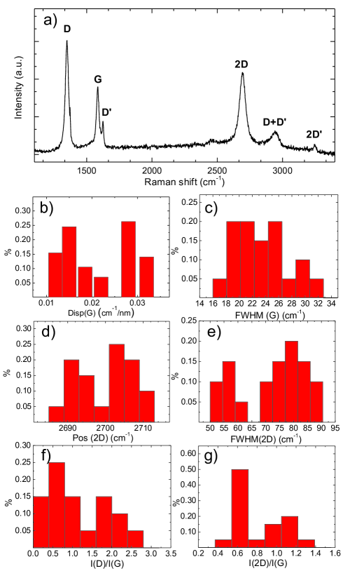
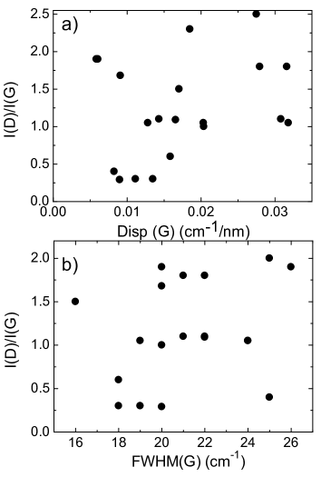
We assign the D and D’ peaks to the edges of the sub-micrometer flakesCasiraghi2009 , rather than to the presence of a large amount of disorder within the flakes. This is further supported by the plot of the G peak dispersion, Disp(G)(Fig.3b)). This is defined as Disp(G) = , where is the laser excitation wavelength. Disp(G) is generated from the linear fit the plot of the G peak position, Pos(G), as a function of the laser excitation wavelength. In disordered carbons Pos(G) increases as the excitation wavelength decreases, from IR to UVFerrari2000 , thus Disp(G) increases with disorderFerrari2001 ; Ferrari2000 . The full width at half maximum of the G peak, FWHM(G), always increases with disorderFerrari2003 ; Cancado2011 . Thus, combining the intensity ration of the D and G peaks, I(D)/I(G), with FWHM(G) and Disp(G) allows us to discriminate between disorder localized at the edges, and disorder in the bulk of the samples. In the latter case, to higher I(D)/I(G) would correspond higher FWHM(G) and Disp(G). Figs.4 a,b) show that Disp(G), I(D)/I(G) and FWHM(G) are not correlated, a clear indication that the major contribution to the D peak comes from the sample edges. Also, Disp(G) is nearly zero for all samples, compared to the values bigger than 0.1cm-1/nm expected for disordered carbonsFerrari2001 ; Ferrari2004 , another indication of the lack of large structural disorder within our flakes. The distribution of 2D peak positions, Pos(2D), shown in 3d, has two maxima2692 and 2705cm-1, similar to FWHM(2D) (3e). This is consistent with the samples being a distribution of SLG, BLG and FLGs, but with a significant fraction of SLGs. We note that for the flakes with the smallest Pos(2D) and FWHM(2D), the ration of the 2D and G integrated areas, A(2D)/A(G), is at most 3.5, implying a doping of at least 1013cm-2.Basko2009 ; Das2008 ; Pisana2007
We now estimate , and for our ink, in order to check its viability for ink-jet printing. can be evaluated as (1+2.5)Kaye1997 ; Derby2003 , where is the viscosity of the pure solvent and the volume fraction of particles in the dispersion. We assume 0.8mPas, the viscosity of pure NMP at 80∘CHandchemLide ; Kauffman2001 (the temperature of the drops ejected from our printer, as specified in Ref. Epson2011, ). We take =1-, where VolNMP [0.972 mm3] is the volume of 1mg pure NMP and Volink [0.94 mm3] is the volume of 1mg of our ink, both measured by a micropipette (2nL precision), at room temperature and pressure. We thus get 0.03, and 0.96mPas. From the same measurement we also obtain 1.06gcm-3 and derive 50mJ m-2 from tensiometer measurements. Given these parameters, and our nozzle diameter50m, we get Z1.7, which falls within the range suitable for printingReis2000 ; Jang2009 , but close to the lower boundary of allowed Z,Fromm1984 ; Reis2000 ; Jang2009 thus implying a lower probability of secondary drops ejectionReis2000 ; Kaye1997 ; Derby2003 . However, high viscosity may generate nanoparticle re-aggregationKaye1997 .
III.2 Ink-jet printed features
The final layout of printed nano-particle inks depends on substrate SEdeGans2004 ; van Osch2008 , ink viscosity and surface tensiondeGans2004 .
To investigate the influence of surface treatments, we print our ink on pristine, HMDS coated and O2 plasma treated Si/SiO2. A modified Epson Stylus 1500 ink-jet printer equipped with an Epson S020049 cartridge is used to print the dispersions under a constant nitrogen flow, followed by annealing at 170∘C for 5 minutes to remove the NMP. The nozzle is placed1mm above the substrate. HMDS is deposited by spin coating for 40s at 1000rpm, followed by annealing at 80∘C for 2 min. Alternatively the substrates are cleaned by a RF O2 plasma at 200W and 410-1 Torr for 2 min.
We use optical micrographs to visualize the ink-jet printed drops, Figs.5a,b,c. The bright green/blue color of the printed features is due to the use of dark field imaging. These reveal that HMDS constrains the drops to 90m diameter (Fig.5c), smaller than on the other substrates (100m and 150m for pristine, Fig.5b, and plasma treated SiO2, Fig.5a). As discussed above, we use NMP as solvent to reduce the coffee ring effect compared to low boiling point solvents (e.g. water, chloroform)Deegan1997 ; Derby2003 ; Singh2010 . However, we still observe coffee-rings when printing on pristine SiO2 (Fig.5b), while Fig.5c reveals a higher flake uniformity, and no coffee-rings on HMDS treated SiO2. Fig.5d a representative printed pattern, showing the ability to fabricate complex layouts.
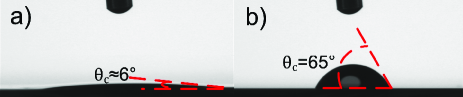
Thus, HMDS appears to prevent coffee-rings. To understand this, we measure the substrates SE and investigate the printed stripes morphology, before and after surface treatment. We perform contact angle measurements with a A KSV CAM200 system. The contact angle is measured by dispensing 1l DI water on the substrates. The surface tension is measured by the DuNouy-Padday techniquePadday1971 . This consists in using a rod few millimeters diameter immersed in the dispersion, followed by pull out. The rod is attached to a scale or balance via a thin metal hook that measures the maximum pull force. This is recorded as the probe is first immersed 1mm into the solution and then slowly withdrawn from the interface. The contact angle, , depends on the liquid surface tensionShafrin1960 ; deGennes1985 ; Israelachvili1991 and the substrate critical surface tensionShafrin1960 ; deGennes1985 ; Israelachvili1991 , according to the Young’s relationdeGennes1985 ; Israelachvili1991 ; Young1805 : --cos=0, where [mJ m-2] is the solid-vapor surface tension, is the solid-liquid surface tension and is the liquid-vapor surface tension.
Figs.6a,b show ink drops printed onto pristine and HMDS treated Si/SiO2, with 6∘ and65∘, indicating that the pristine substrate SE is modified following HMDS treatment. was measured73mJ m-2 in Ref.Shafrin1967, for DI water, whereas 116.5mJ m-2 and40mJ m-2 were reported for pristineThomas1996 and HMDS treatedGlendinning1991 Si/SiO2. Consequently, 43.9mJ m-2 and 9.1mJ m-2 for pristine and HMDS treated Si/SiO2, respectively. A higher implies a higher SEGhatee2005 . Indeed, our correspond to SEs73.9 and39.1mJ m-2 for pristine and HMDS treated Si/SiO2. A small results in the drop rapid spreading on the substratedeGennes1985 , as seen in pristine SiO2. On the other hand, HMDS provides higher , since it lowers (thus the substrate SE), therefore reducing the wettabilityMarmur2003 ; Shafrin1960 .
When ink-jet printing stripes, the inter-drop (i.e. centre to centre) distance is an important parameterDuineveld2003 . For a large distance, individual drops are deposited on the substrateDuineveld2003 ; Reis2000 ; Derby2003 . As the inter-drop distance decreases, these merge into a lineDuineveld2003 . Thus, in order to obtain a continuous line we need an inter-drop distance smaller than the drop diameterDuineveld2003 . On the other hand, Refs.Kaye1997, ; Derby2003, reported that a very small inter-drop distance can result in particle aggregation on the substrate, thus a non-uniform stripe (i.e. irregular edges). We thus select an inter-drop distance suitable to have continuous lines, avoiding at the same time non-uniformities and irregular edges.
Figs.7a,b,c are optical images of printed stripes on pristine, O2 plasma treated and HMDS treated Si/SiO2, whereas Figs.7d,e,f plot the respective Atomic Force Microscope (AFM) topographies. The stripe in Fig.7a is100-110m wide, has an average thickness70nm and an irregular flake distribution, with aggregation of flakes. That in Fig.7b is wider (130-140m), with aggregates at the edges, and an average thickness55nm. The stripe in Fig.7c has a more uniform and regular distribution of flakes,85-90m wide and90nm thick. The width narrows going from the O2 plasma treated to the HMDS treated Si/SiO2, due to the SE decrease. Figs.7d,e show stripes with voids and irregular flake distribution, with R30-40nm. Fig.7f presents a more homogeneous network with R15nm. Thus, Rz is lower when is higher, because the poor wettability of drops with higher reduces the stripe diameter (as shown in Figs.7a,b,c), confining the flakes onto a smaller area. The uniformity of stripes printed on the HMDS treated substrate corroborates the above considerations on the SE changes. In fact, the presence of silane in HMDSOsthoff2007 promotes the adhesion of metallic particles to the substrateOsthoff2007 ; Gamerith2007 . Analogously, HMDS may promote the adhesion of graphene to the substrate, thus resulting in a uniform network.
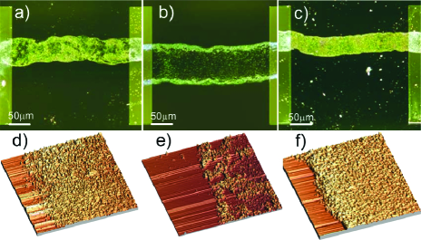
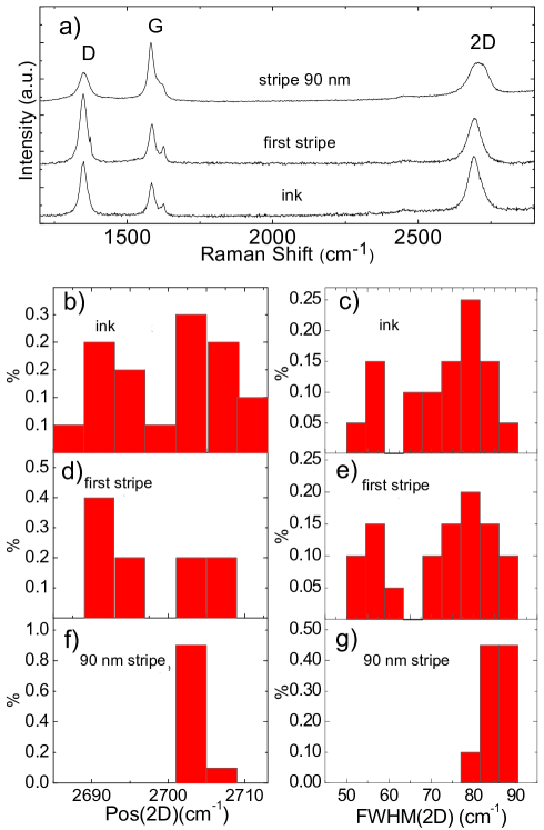
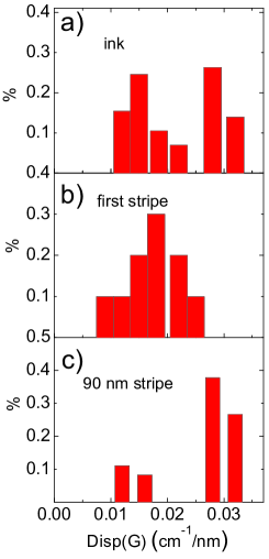
Fig.8a compares a typical Raman spectrum of a flake in the ink, with a measurement on the first stripe and on a stripe 90 nm thick, after 30 printing repetitions. Figs.8b,c,d,e,f,g,9 compare the Pos(2D), FWHM(2D) and Disp(G) distributions. The data show that the first stripe has very similar characteristics to the ink, as expected. However, the spectra after 90 repetitions show a Pos(2D) and FWHM(2D) distribution more typical of a multi-layer sample, having lost any direct signature of SLG. Note however that the 2D peak shape, even for the 90nm stripe, remains distinctly different from that of graphite. A similar aggregation of flakes was previously observed for thick films derived from graphene solutionsHernandez2008 . In all cases Disp(G) remains similar, and very low, again showing the lack of large amounts of defects within the flakes.
III.3 Transparent and conductive patterns
We now investigate the viability of our ink to print transparent and conductive patterns. We characterize the sheet resistance Rs [/] and Transmittance T [%] of our stripes when placed on a transparent substrate. We thus use pristine, O2 and HMDS treated borosilicate glass, with Rz15nm similar to SiO2 on Si, but with T99% (Pyrex 7740-Polished Prime Grade). T is measured on samples ink-jet printed on borosilicate glass (followed by annealing at 170∘C for 5 mins to remove the NMP) by scanning a 514.5nm laser beam with 100m steps. The transmitted beam is measured with a photodiode. A microscope equipped with 100 long distance objective focuses the laser to2m. The incident power is kept at8mW. The transmitted power is measured by a Ophir Nova II power meter with 0.1W resolution.
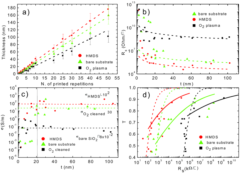
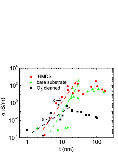
Fig.10a shows that for our stripes the experimentally measured thickness (t) increases linearly as a function of printing repetitions, with a slope defined by the surface treatment. Fig.10b plots the four-probe measured Rs as a function of t. For large t, Rs settles to34,500,105k/ for HMDS treated, pristine and O2 treated glass, respectively. For t20nm, Rs increases for all substrates. For a thin film, R, where [S/m] its conductivitySmits1958 . Thus, from Fig.10b and =(R, we get the data in Fig.10c. is constant for t20nm, in the case of HMDS treated, pristine and plasma treated glass, with an average102,30,10-1S/m, respectively. Thus, stripes on HMDS treated glass have an higher combined with a more regular network of flakes, compared to the other two substrates. When t20nm, decreases for all substrates. A similar trend was reported for CNT films on SiO2 (produced by vacuum filtration)Hu2004 ; Geng2007 , ink-jet printed CNT patterns on SiO2Takenobu2009 ; Okimoto2010 , graphene films on SiO2,DeSmall2009 ; DeACS2010 and Polyethylene-terephthalate(PET),DeSmall2009 ; DeACS2010 as well as Ag nanowire films, produced by vacuum filtration on SiO2DeACS2010 . Refs. Hu2004, ; Geng2007, ; DeSmall2009, ; DeACS2010, explained this decrease of for small t, due to percolation.
The percolation theoryKirkpatrick1973 predicts , for a network of conductive particles, to scale asKirkpatrick1973 :
| (1) |
where [g/mm2] is the concentration of conductive particles per unit area, [g/mm2] is the critical concentration of flakes corresponding to the percolation threshold and is the percolation exponent. Eq.1 can be rewritten in terms of t, rather than Hu2004 as:
| (2) |
where is the critical thickness and is the percolation exponent. Fig.10c shows two regimes for as a function of t: a percolative linear behavior for t20nm and a constant for t20nm. This can be explained considering that our films stop behaving like bulk materials below a critical thickness ().
The exponent can be estimated by a linear fit of the log10 plot of vs t, in the percolation region (t20nm), Fig.11. We get 4 for stripes on HMDS treated and pristine glass, while 3 for O2 treated glass. These values indicate percolation, as reported by Refs.Kogut1979, ; Stauffer1985, ; Johner2008, ; DeACS2010, for networks with various geometries. is expected to increase with particle sizeKogut1979 ; Johner2008 and decrease with Kogut1979 ; Johner2008 . Assuming a similar particle size, since the same ink is used for all cases, we deduce that 4 points to a bigger than 3. This indicates formation of a more uniform network on HMDS treated and pristine glass compared to O2 treated glass.
We also determine the minimum concentration necessary to achieve the bulk conductivity regime. To do so, we assume XXC, because the bulk regime needs a tight network of interconnected flakesStauffer1985 ; Doherty2009 ; DeACS2010 . Given our 0.11g/L, volume per printed drop10nLEpson2011 , and a dried drop size on the three substrates of90,100,130m, we estimate 410-2,10-2 and0.710g/mm2 for stripes printed on HMDS, pristine and plasma treated glass, respectively. Consequently, from Eq.1, for stripes on HMDS treated glass (102S/m) is higher than on pristine (40S/m) and plasma treated glass(0.1S/m).
Fig.10d shows T as a function of Rs. The dashed lines are a plot of the relation T= expected for stripes with conductivity, where Z0=377 is the free-space impedance, G610 is the universal optical conductance of grapheneKuzmenko2008 . The solid lines are a plot of T= expected in the percolative regimeDeACS2010 , where is the percolative Figure of Merit . Our experimental T deviates from the dashed lines for T75%. We assign this to the percolative regime where deviates from a bulk-like behavior. Also in this case, printing on HMDS treated glass gives the highest T for a given Rs.
III.4 Ink jet printed devices
Ink-jet printed TFTs based on organic semiconducting polymers have been widely investigatedSirringhaus2000 ; Ong2004 ; Arias2004 . The current state of the art devices have ranging from 0.01 to0.5cm2V-1s-1, with ON/OFF ratios up to 105.Ong2004 ; Arias2004 ; Wu2005 Several Inkjet printed TFTs using various carbon nanomaterials have been reported. For example, fullerene-based TFTs were discussed in Refs. Kaneto2007, ; Morita2010, , with up to 0.01cm2V-1s-1 and an ON/OFF ratio10. TFTs printed from CNT-based inks have been presented by several groupsBeecher2007 ; Hsieh2009 ; Takenobu2009 ; Okimoto2009 ; Ha2010 . The highest thus far is50cm2V-1s-1 combined with an ON/OFF ratio 103, but measured at 10-6 Torr and 100KHa2010 . Ink-jet printed TFTs from GO-based inks were discussed in Refs. Dua2010, ; Wang2009, , with up to90cm2V-1s-1 for an ON/OFF ratio of 10 (measured at room conditions), after GO reduction.
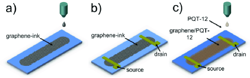
We print our TFTs as for Fig.12a, and contact them with chromium-gold source and drain pads (Fig.12b). The transfer characteristics are measured (at room conditions) at different drain voltages (Vd=-2,-4,-8V). is derived from =, where L [m] and W [m] are the channel length and width respectively, Ci is the gate dielectric capacitance (10nF/cm2)Oh2009 . We get 95cm2V-1s-1 for an ON/OFF ratio10 at Vd=-2V, comparable to that reported in Ref. Wang2009, for ink-jet printed RGO TFTs. in our devices is almost four orders of magnitude higher than printed fullerene-based TFTsKaneto2007 ; Morita2010 (for the same ON/OFF ratio) and more than two orders higher than ink-jet printed CNTsBeecher2007 ; Takenobu2009 (for a ON/OFF ratio of 10). However, the ON/OFF ratio in our TFTs is lower than the state of the art for CNTs (but measured at 10-6 Torr and 100K) at similar Ha2010 . We note that ink-jet printed electronics requires high at room conditionsSingh2010 ; Singh2006 . So far CNT ink-jet printed devices measured at room conditions have no larger than 1cm2V-1s-1 (at ON/OFF10)Takenobu2009 , which is two orders of magnitude smaller than our jet printed TFTs.
Organic semiconducting inksOng2004 ; Arias2004 ; Wu2005 suffer from low , limited by variable range hopping between the isolated polymer chainsSirringhaus1998 . The overall charge conduction in crystalline organic semiconducting thin films is determined by both intra-chain and inter-chain charge transportSong2010 . The former is much faster than inter-chain hoppingSong2010 ; Sirringhaus1998 . Many groups have tried to improve interchain hoppingWhiting2009 ; Klauk_book2006 ; Beecher2007 ; Hsieh2009 . Ref. Whiting2009, proposed a chemical modification of the semiconducting organic ink by electron acceptors, while embedding Au nano-particles in the semiconducting organic ink was proposed by Ref. Klauk_book2006, . Embedding CNTs in the semiconducting inkBeecher2007 ; Hsieh2009 allowed us to get V-1s-1 at room conditions.
We combine our graphene-ink with one of the most commonly used organic polymers for ink-jet printing, Poly[5,5’-bis(3-dodecyl-2-thienyl)-2,2’-bithiophene] (PQT-12)Ong2004 ; Arias2004 ; Wu2005 in order to investigate its viability as interchain hopping enhancer (similarly to Au nanoparticles and CNTs). PQT-12 is widely used due to the higher environmental stability (up to 300 days at room conditionsChason2005 ), with respect to other organic semiconducting inksKlauk_book2006 ; Chason2005 . Graphene can bridge the polymer chains, allowing a more efficient charge transport.
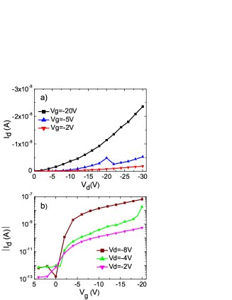
We fabricate a graphene/PQT-12 TFT following the steps shown in Figs.12a,b,c. Fig.13a plots its output characteristics at Vg=-2,-5,-20 V. For each Vg, Vd is swept from 0 to -30 V in steps of 2V. At Vd=-2V, we get 0.17cm2V-1s-1 and an ON/OFF ratio4105. This is about ten times that of ink-jet printed CNTs/PQT-12 TFTsBeecher2007 ; Hsieh2009 at ON/OFF105. When compared to pure organic semiconducting polymers, our is 20 times higher than ink-jet printed PQT-12Arias2004 ; Wu2005 , and twice the highest reported for ink-jet printed TFTs made of pure (Poly(2,5-bis(3-tetradecyllthiophen-2-yl)thieno[3,2-b]thiophene)Kawase2005 ; Klauk_book2006 ; Parmer2008 ; Singh2010 . Thus, the combination of our graphene-ink with organic semiconducting inks is promising for high performance printed electronics.
IV Conclusions
We demonstrated ink-jet printing of graphene. Liquid phase exfoliated graphene is an ideal and low cost material for the fabrication of transparent conductive inks. Our graphene-ink was used to print TFTs with up to95cm2V-1s-1. It was also combined with PQT-12 to fabricate devices with 0.2cm2V-1s-1 and ON/OFF ratios4105. This demonstrates the viability of graphene-inks for flexible and transparent electronics.
V acknowledgements
We acknowledge funding from the Royal Society Brian Mercer Award for Innovation, the ERC grant NANOPOTS, EPSRC grants EP/GO30480/1 and EP/F00897X/1, EU Grants RODIN and GENIUS, King’s college, Cambridge. ACF is a Royal Society Wolfson Research Merit Award holder.
References
- (1) Q. Cao, H. S. Kim, N. Pimparkar, J. P. Kulkarni, C. J. Wang, M. Shim, K. Roy, M. A. Alam, J. A. Rogers, Nature 454, 495 (2008).
- (2) L. Zhou, A. Wanga, S.C. Wu, J. Sun, S. Park, T. N. Jackson, Appl. Phys. Lett. 88, 083502 (2006).
- (3) I. Ota, J. Ohnishi and M. Yoshiyama, M. Proc. IEEE 61, 832 (1973).
- (4) G. H. Gelinck, H. E. A. Huitema, E. van Veenendaal, E. Cantatore, L. Schrijnemakers, J. B. P. H. van der Putten, T. C. T. Geuns, M. Beenhakkers, J. B. Giesbers, B.-H. Huisman, E. J. Meijer, E. M. Benito, F. J. Touwslager, A. W. Marsman, B. J. E. van Rens, D. M. de Leeuw, Nat. Mater. 3, 106 (2004).
- (5) T. Sekitani, T. Yokota, U. Zschieschang, H. Klauk, S. Bauer, K. Takeuchi, M. Takamiya, T. Sakurai, T. Someya, Science 326, 1516 (2009).
- (6) K. Myny, S. Steudel, P. Vicca, M. J. Beenhakkers, N. A. J. M. van Aerle, G. H. Gelinck, J. Genoe, W. Dehaene, P. Heremans, Solid State Electron. 53, 1220 (2009).
- (7) C. G., Granqvist, Sol. Energ. Mat. Sol. C. 91, 1529 (2007).
- (8) J. Yoon, A. J. Baca, S.-I. Park, P. Elvikis, J. B. Geddes, L. Li, R. H. Kim, J. Xiao, S. Wang, T.-H. Kim, M. J. Motala, B. Y. Ahn, E. B. Duoss, J. A. Lewis, R. G. Nuzzo, P. M. Ferreira, Y. Huang, A. Rockett, J. A. Rogers, Nat. Mater. 7, 907 (2008).
- (9) B. Schmied, J. Gunther, C. Klatt, H. Kober, E. Raemaekers, Smart Textiles 60, 67 (2009).
- (10) D. Kim, A. Jong-Hyun, K. Hoon-Sik, L. Keon Jae, K. Tae-Ho, Y. Chang-Jae, R. G. Nuzzo, J. A. Rogers, IEEE Electr. Device Lett. 29, 73 (2008).
- (11) T. B. Singh, N. S. Sariciftci, Annu. Rev. Mater. Res. 36, 199 (2006).
- (12) J. A. Rogers, Z. Bao, K. Baldwin, A. Dodabalapur, B. Crone, V. R. Raju, V. Kuck, H. Katz, K. Amundson, J. Ewing, P. Drzaic, P. Natl. Acad. Sci. U.S.A. 98, 4835 (2001).
- (13) S. R. Forrest, Nature 428, 911 (2004).
- (14) Z. Bao, J. A. Rogers, H. E. Katz, J. Mater. Chem. 9, 1895(1999).
- (15) H. Sirringhaus, T. Kawase, R. H. Friend, T. Shimoda, M. Inbasekaran, W. Wu, E. P. Woo, Science 290, 2123 (2000).
- (16) Y. G. Sun, E. Menard, J. A. Rogers, H. S. Kim, S. Kim, G. Chen, I. Adesida, R. Dettmer, R. Cortez, A. Tewksbury, Appl. Phys. Lett. 88, 3 (2006).
- (17) M. C. McAlpine, R. S. Friedman, C. M. Lieber, Proc. IEEE 93, 1357 (2005).
- (18) M. Singh, H. M. Haverinen, P. Dhagat, G. E. Jabbour, Adv. Mater. 22, 673 (2010).
- (19) P. Peumans, S. Uchida, S. R. Forrest, Nature 425, 158 (2003).
- (20) P. Servati, A. Nathan, Proc. IEEE 93, 1257(2005).
- (21) B. J., DeGans, P. Duineveld, U. Schubert, Adv. Mater. 16, 203 (2004).
- (22) H. M. Dong, W. W. Carr, J. F. Morris, Phys. Fluids 18, 16 (2006).
- (23) T. H. J. van Osch, J. Perelaer, A. W. M. de Laat, U. S. Schubert, Adv. Mater. 20, 343 (2008).
- (24) J. E. Yoo, K. S. Lee, A. Garcia, J. Tarver, E. D. Gomez, K. Baldwin, Y. Sun, H. Meng, T.Q. Nguyen, Y.L. Loo, Proc. Natl. Acad. Sci. U.S.A. 107, 5712 (2010).
- (25) T. Shimoda, Y. Matsuki, M. Furusawa, T. Aoki, I. Yudasaka, H. Tanaka, H. Iwasawa, D. Wang, M. Miyasaka, Y. Takeuchi, Nature 440, 783 (2006).
- (26) Y. Y. Noh, X. Cheng, H. Sirringhaus, J. I. Sohn, M. E. Welland, D. J. Kang, Appl. Phys. Lett. 91, 043109 (2007).
- (27) P. Beecher, P. Servati, A. Rozhin, A. Colli, V. Scardaci, S. Pisana, T. Hasan, A. J. Flewitt, J. Robertson, G. W. Hsieh, F. M. Li, A. Nathan, A. C. Ferrari, W. I. Milne, J. Appl. Phys. 102, 043710 (2007).
- (28) G. W. Hsieh, F. M. Li, P. Beecher, A. Nathan, Y. L. Wu, B. S. Ong, W. I. Milne, J. Appl. Phys. 106, 7 (2009).
- (29) T., Takenobu, N. Miura, S.Y. Lu, H. Okimoto, T. Asano, M. Shiraishi, Y. A. Iwasa, App. Phys. Expr. 2, 025005 (2009).
- (30) H. Okimoto, T. Takenobu, K. Yanagi, Y. Miyata, H. Shimotani, H. Kataura, Y. Iwasa, Adv. Mater. 22, 3981(2010).
- (31) H. Okimoto, T. Takenobu, K. Yanagi, Y. Miyata, H. Kataura, T. Asano, Y. Iwasa, J. J. App. Phys. 48, 4 (2009).
- (32) M. Ha, Y. Xia, A. A. Green, W. Zhang, M. J. Renn, C. H. Kim, M. C. Hersam, C. D. Frisbie, ACS Nano 4, 4388 (2010).
- (33) N. Luechinger, A., E. K. Athanassiou, W. J. Stark, Nanotechnol. 19, 445201 (2008).
- (34) A. K. Geim, K. S. Novoselov, Nat. Mater. 6, 183 (2007).
- (35) K. S. Novoselov, A. K. Geim, S. V. Morozov, D. Jiang, Y. Zhang, S. V. Dubonos, I. V. Grigorieva, A. A. Firsov, Science 306, 666 (2004).
- (36) J. C. Charlier, P. C. Eklund, J. Zhu, A. C. Ferrari, Topics Appl. Phys. 111, 673 (2008).
- (37) F. Bonaccorso, Z. Sun, T. Hasan, A. C. Ferrari, Nat. Photon. 4, 611 (2010).
- (38) Y. M. Lin, C. Dimitrakopoulos, K. A. Jenkins, D. B. Farmer, H. Y. Chiu, A. Grill, P. Avouris, Science 327, 662 (2010).
- (39) Z. Sun, T. Hasan, F. Torrisi, D. Popa, G. Privitera, F. Wang, F. Bonaccorso, D. M. Basko, A.C. Ferrari, ACS Nano 4, 803 (2010).
- (40) K. S. Novoselov, D. Jiang, F. Schedin, T. J. Booth, V. V. Khotkevich, S. V. Morozov, A. K. Geim, PNAS 102, 10451 (2005).
- (41) A. E. Karu,M. Beer, J. Appl. Phys. 37, 2179 (1966).
- (42) A. N. Obraztsov, E. A. Obraztsova, A. V. Tyurnina, A. A. Zolotukhin, Carbon 45, 2017 (2007).
- (43) K. S. Kim, Y. Zhao, H. Jang, S. Y. Lee, J. M. Kim, K. S. Kim, J.-H. Ahn, P. Kim, J.Y. Choi, B. H. Hong, Nature 457, 706 (2009).
- (44) A. Reina, X. Jia, J. Ho, D. Nezich, H. Son, V. Bulovic, M. S. Dresselhaus, J. Kong, Nano Lett. 9, 30 (2009).
- (45) X. S. Li, W. W. Cai, J. H. An, S. Kim, J. Nah, D. X. Yang, R. Piner, A. Velamakanni, I. Jung, E. Tutuc, S. K. Banerjee, L. Colombo, R.S. Ruoff, Science 324, 1312 (2009).
- (46) S. Bae, H. Kim, Y. Lee, X. Xu, J.-S. Park, Y. Zheng, J. Balakrishnan, T. Lei, H. Ri Kim, Y. I. Song, Y.J. Kim, K. S. Kim, B. Ozyilmaz, J.H. Ahn, B. H. Hong,S. Iijima, Nat. Nano. 5, 574 (2010).
- (47) C. Berger, Z. M. Song, X. B. Li, X. S. Wu, N. Brown, C. Naud, D. Mayou, T. B. Li, J. Hass, A. N. Marchenkov, E. H. Conrad, P. N. First,W. A. de Heer, J. Phys. Chem. B 108, 19912 (2006).
- (48) E. G. Acheson, US patent 615 (1896).
- (49) D. V. Badami, Nature 193, 569 (1962).
- (50) K. V. Emtsev, A. Bostwick, K. Horn, J. Jobst, G. L. Kellogg, L. Ley, J. L. McChesney, T. Ohta, S. A. Reshanov, J. Rohrl, E. Rotenberg, A. K. Schmid, D. Waldmann, H. B. Weber,T. Seyller, Nat. Mater. 8, 203 (2009).
- (51) C. Oshima, A. Nagashima, J. Phys.: Condens. Matter 9, 1 (1997).
- (52) Y. Gamo, A. Nagashima, M. Wakabayashi, M. Terai, C. Oshima, Surf. Sci. 374, 61 (1997).
- (53) R. Rosei, M. De Crescenzi, F. Sette, C. Quaresima, A. Savoia, P. Perfetti, Phys. Rev. B 28, 1161 (1983).
- (54) P. W. Sutter, J. I. Flege, E. A. Sutter, Nat. Mater. 7, 406 (2008).
- (55) Y. Hernandez, V. Nicolosi, M. Lotya, F. M. Blighe, Z. Sun, S. De, I. T. McGovern, B. Holland, M. Byrne, Y. K. Gun’Ko, J. J. Boland, P. Niraj, G. Duesberg, S. Krishnamurthy, R. Goodhue, J. Hutchison, V. Scardaci, A. C. Ferrari, J. N. Coleman, Nat. Nanotech. 3, 563 (2008).
- (56) M. Lotya, Y. Hernandez, P. J. King, R. J. Smith, V. Nicolosi, L. S. Karlsson, F. M. Blighe, S. De, Z. Wang, I. T. McGovern, G. S. Duesberg, J. N. Coleman, J. Am. Chem. Soc. 131, 3611 (2009).
- (57) C. Valles, C. Drummond, H. Saadaoui, C. A. Furtado, M. He, O. Roubeau, L. Ortolani, M. Monthioux and A. Penicaud, J. Am. Chem. Soc 130, 15802 (2008).
- (58) T. Hasan, F. Torrisi, Z. Sun, D. Popa, V. Nicolosi, G. Privitera, F. Bonaccorso, A. C. Ferrari, Phys. Stat. Sol. B 247, 2953 (2010).
- (59) O. M. Marago, P. H. Jones, F. Bonaccorso, V. Scardaci, P. G. Gucciardi, A. G. Rozhin, A. C. Ferrari, ACS Nano 4, 7515 (2010).
- (60) A. A. Green, M. C. Hersam, Nano Lett. 9, 4031 (2009).
- (61) X. L. Li, X. R. Wang, L. Zhang, S. W. Lee, H. J. Dai, Science 319, 1229 (2008).
- (62) S. Stankovich, R. D. Piner, S. T. Nguyen, R. S. Ruoff, Carbon 44, 3342 (2006).
- (63) W. S. Hummers, R. E. Offeman, J. Am. Chem. Soc. 80, 1339 (1958).
- (64) B. C. Brodie, Ann. Chim. Phys. 59, 466 (1860).
- (65) L. Staudenmaier, Ber. Deut. chem. Ges. 31, 1481 (1898).
- (66) C. Mattevi, G. Eda, S. Agnoli, S. Miller, K. A. Mkhoyan, O. Celik, D. Mastrogiovanni, G. Granozzi, E. Garfunkel, M. Chhowalla, Adv. Funct. Mater. 29, 2577 (2009).
- (67) W. W. Cai, R. D. Piner, F. J. Stadermann, S. Park, M. A. Shaibat, Y. Ishii, D. X. Yang, A. Velamakanni, S. J. An, M. Stoller, J. H. An, D. M. Chen, R. S. Ruoff, Science 321, 1815 (2008).
- (68) G. Eda, M. Chhowalla, Adv. Mater. 22, 2392 (2010).
- (69) J. I., Paredes, S. Villar-Rodil, A. Martinez-Alonso, J. M. D. Tascon, Langmuir, 24, 10560 (2008).
- (70) H., He, J. Klinowski, M. Forster, A. Lerf, Chem. Phys. Lett., 287, 53 (1998).
- (71) G. Eda, G. Fanchini, M. Chhowalla, Nat. Nanotech. 3, 270 (2008).
- (72) V. Dua, S. Surwade, S. Ammu, S. Agnihotra, S. Jain, K. Roberts, S. Park, R. Ruoff, S. Manohar, Angew. Chem. Int. Ed. 49, 2154 (2010).
- (73) S. Wang, P. K. Ang, Z. Wang, A. L. L. Tang, J. T. L. Thong, K. P. Loh, Nano Lett. 10, 92 (2009).
- (74) B. K. Park, D. Kim, S. Jeong, J. Moon, J. S. Kim, Thin Solid Films 515, 7706 (2007).
- (75) N. Reis, B. Derby, MRS. Symp. Proc. 624, 65 (2000).
- (76) D. Jang, D. Kim and J. Moon, Langmuir 25, 2629 (2009).
- (77) J. E. Fromm, IBM J. Res. Dev., 28, 322 (1984).
- (78) http://www.microfab.com/equipment/technotes/technote99-02.pdf.
- (79) P. G. De Gennes, Rev. Mod. Phys. 57, 827 (1985).
- (80) E. G. Shafrin, W. A. Zisman, J. Phys. Chem. 64, 519 (1960).
- (81) J. Israelachvili, Intermolecular and Surface Forces; Academic press, New York, (1991).
- (82) B. Derby, N. Reis, MRS. Bull. 28, 815 (2003).
- (83) J. S. Park, J. P. Kim, C. Song, M. Lee, J. S. Park, J. P. Kim, C. Song, M. Lee, Displays 31, 164 (2010).
- (84) R. D. Deegan, O. Bakajin, T. F. Dupont, G. Huber, S. R. Nagel, T. A. Witten, Nature 389, 827 (1997).
- (85) R. C. Osthoff, S.W. Kantor, Organosilazane Compounds John Wiley & Sons, Inc.; (1997)
- (86) D. R. Lide, In Handbook of Chemistry and physics 86th ed.; CRC Press Inc.; Boca Raton, FL, (2005)
- (87) K. F. Mak, M. Y. Sfeir, Y. Wu, C. H. Lui, J. A. Misewich,T. F. Heinz, Phys. Rev. Lett. 101, 196405 (2008).
- (88) V. G. Kravets, A. N. Grigorenko, R. R. Nair, P. Blake, S. Anissimova, K. S. Novoselov, A. K. Geim, Phys. Rev. B 81, 155413 (2010).
- (89) R. R. Nair, P. Blake, A. N. Grigorenko, K. S. Novoselov, T. J. Booth, T. Stauber, N. M. R. Peres, A. K. Geim, Science 320, 1308 (2008).
- (90) C. Casiraghi, A. Hartschuh, E. Lidorikis, H. Qian, H. Harutyunyan, T. Gokus, K. S. Novoselov, A. C. Ferrari, Nano Lett., 7, 2711 (2007).
- (91) J. C. Meyer, A. K. Geim, M. I. Katsnelson, K. S. Novoselov, T. J. Booth, S. Roth, Nature 446, 60 (2007).
- (92) J. C. Meyer, A. K. Geim, M. I. Katsnelson, K. S. Novoselov, D. Obergfell, S. Roth, C. Girit, A. Zettl, Solid State Commun. 143, 101 (2007).
- (93) A. C. Ferrari, J. C. Meyer, V. Scardaci, C. Casiraghi, M. Lazzeri, F. Mauri, S. Piscanec, D. Jiang, K. S. Novoselov, S. Roth, A. K. Geim, Phys. Rev. Lett. 97, 4 (2006).
- (94) U. Khan, A. O’Neill, M. Lotya, S. De, J. N. Coleman, Small 6, 864 (2010).
- (95) C. M. Hansen, Hansen Solubility Parameters: A User’s Handbook, CRC Press Inc., Boca Raton, FL (2007)
- (96) S. D. Bergin, V. Nicolosi, P. V. Streich, S. Giordani, Z. Sun, A. H. Windle, P. Ryan, N. P. P. Niraj, Z.-T. Wang, L. Carpenter, W. J. Blau, J. J. Boland, J. P. Hamilton, J. N. Coleman Adv. Mater. 20, 1876 (2008).
- (97) M. Lotya, P. J. King, U. Khan, S. De, J. N. Coleman, ACS Nano 4, 3155 (2010).
- (98) J. W. Williams, K. E. Van Holde, R. L. Baldwin, H. Fujita, Chem. Rev. 58, 715 (1958).
- (99) P. Schuck, Biophys. J. 78, 1606 (2000).
- (100) T. Svedberg, K. O. Pedersen, The Ultracentrifuge, Oxford University press, London (1940)
- (101) A. C. Ferrari, J. Robertson, Phys. Rev. B 61, 14095 (2000).
- (102) F. Tuinstra, J. L. Koenig, J. Chem. Phys. 53, 1126 (1970).
- (103) S. Piscanec, M. Lazzeri, F. Mauri, A. C. Ferrari, J. Robertson, Phys. Rev. Lett. 93, 4 (2004).
- (104) C. Casiraghi, A. Hartschuh, H. Qian, S. Piscanec, C. Georgi, A. Fasoli, K. S. Novoselov, D. M. Basko, A. C. Ferrari, Nano Lett. 9, 1433 (2009).
- (105) A. C. Ferrari, J. Robertson, Phys. Rev. B 64, 13 (2001).
- (106) L.G. Cancado, A. Jorio, E. H. Ferreira, F. Stavale, C. A. Achete, R. B. Capaz, M. V. O. Moutinho, A. Lombardo, T. S. Kulmala, A.C. Ferrari, Nano Lett., 11, 3190 (2011).
- (107) A. C. Ferrari, S. E. Rodil, J. Robertson, Phys. Rev. B 67, 155306 (2003)
- (108) Ferrari A. C., Surf. Coat. Tech. 180-181, 190 (2004).
- (109) D. M. Basko, S. Piscanec, A. C. Ferrari, Phys. Rev. B 80, 165413 (2009).
- (110) A. Das, S. Pisana, B. Chakraborty, S. Piscanec, S. K. Saha, U. V. Waghmare, K. S. Novoselov, H. R. Krishnamurthy, A. K. Geim, A. C. Ferrari, A. K. Sood, Nat. Nano. 3, 210 (2008).
- (111) S. Pisana, M. Lazzeri, C. Casiraghi, K. S. Novoselov, A. K. Geim, A. C. Ferrari, F. Mauri, Nat. Mater. 6, 198 (2007).
- (112) B. H. Kaye, Powder mixing; Chapman & Hall; London, (1997).
- (113) G. W. Kauffman, P. C. Jurs, J. Chem. Inf. Comp. Sci. 41, 408 (2001).
- (114) http://www.epson.com/cgi-bin/Store/Landing/ InkTechCartridges.jsp
- (115) T. Young, Philos. T. R. Soc. Lon. 95, 65 (1805).
- (116) E. G. Shafrin, W. A. Zisman, J. Phys. Chem. 71, 1309 (1967).
- (117) R. R. Thomas, F. B. Kaufman, J. T. Kirleis, R. A. Belsky, J. Electrochem. Soc., 143, 643 (1996).
- (118) W. B. Glendinning, J. N. Helbert, Handbook of VLSI microlithography: principles, technology, and applications, Noyes, New Jersey, (1991).
- (119) M. H. Ghatee, L. Pakdel, Fluid Phase Equilibr. 234, 101 (2005).
- (120) A. Marmur, Langmuir 19, 8343 (2003).
- (121) P. C. Duineveld, J. Fluid Mech. 477, 175 (2003).
- (122) S. Gamerith, A. Klug, H. Scheiber, U. Scherf, E. Moderegger, E. J. W. List, Adv. Func. Mater. 17, 3111 (2007).
- (123) F. M. Smits, Bell Sys. Tech. Jour. 37, 711 (1958)
- (124) L. Hu, D. S. Hecht, G. Gruner , Nano Lett. 4, 2513 (2004).
- (125) H. Z. Geng, K. K. Kim, K. P. So, Y. S. Lee, Y. Chang, Y. H. Lee J. Am. Chem. Soc. 129, 7758 (2007).
- (126) S. De, P.J. King, P.E. Lyons, U. Khan, J. N. Coleman, ACS Nano 4 7064 (2010).
- (127) S. De, J. N. Coleman, Small 6, 458 (2009).
- (128) S. Kirkpatrick, Rev. Mod. Phys. 45, 574 (1973).
- (129) D. Stauffer, A. Aharony, Introduction to percolation theory, Taylor&Francis: London, (1985).
- (130) P. M. Kogut, J. P. Straley, J. Phys. C 12, 2151 (1979).
- (131) N. Johner, C. Grimaldi, I. Balberg, P. Ryser, Phys. Rev. B 77, 174204 (2008)
- (132) E. M. Doherty, S. De, P. E. Lyons, A. Shmeliov, P. N. Nirmalraj, V. Scardaci, J. Joimel, W. J. Blau, J. J. Boland, J. N. Coleman, Carbon 47, 2466 (2009)
- (133) A. B. Kuzmenko, E. Van Heumen, F. Carbone, D. van der Marel, Phys. Rev. Lett. 100, 117401 (2008).
- (134) B. S. Ong, Y. Wu, P. Liu, S. Gardner, J. Am. Chem. Soc. 126, 3378 (2004)
- (135) A. C. Arias, S. E. Ready, R. Lujan, W. S. Wong, K. E. Paul, A. Salleo, M. L. Chabinyc, R. Apte, R. A. Street, Y. Wu, P. Liu, B. Ong, Appl. Phys. Lett. 85, 3304 (2004).
- (136) Y. Wu, P. Liu, B. S. Ong, T. Srikumar, N. Zhao, G. Botton, S. Zhu, Appl. Phys. Lett. 86, 142102 (2005)
- (137) K. Kaneto, M. Yano, M. Shibao, T. Morita, W. Takashima, Jap J. App. Phys. 46, 1736 (2007)
- (138) T. Morita, V. Singh, S. Oku, S. Nagamatsu, W. Takashima, S. Hayase, K. Kaneto, Jap. J. App. Phys. 49, 04161 (2010)
- (139) J. H. Oh, H. W. Lee, S. Mannsfeld, R. M. Stoltenberg, E. Jung, Y. W. Jin, J. M. Kim, J.-B. Yoo, Z. Bao, PNAS 106, 6065 (2009).
- (140) H. Sirringhaus, N. Tessler, R. H. Friend, Science 280, 1741 (1998)
- (141) Y. J. Song, J. U. Lee, W. H. Jo, J. Song, J. U. Lee, W. H. Jo, Carbon 48, 389 (2010)
- (142) G. L. Whiting, A.C. Arias, Appl. Phys. Lett. 95, 253302 (2009)
- (143) H. Klauk, Organic Electronics, Wiley-VCH: Weinheim, (2006); Chapter 4.
- (144) M. Chason, P.W. Brazis, J. Zhang, K. Kalyanasundaram, D. R. Gamota, Proc. IEEE 93, 1348 (2005)
- (145) T. Kawase, S. Moriya, C. J. Newsome, T. Shimoda, Jap. J. App. Phys. 44, 3649 (2005)
- (146) J. E. Parmer, A. C. Mayer, B. E. Hardin, S. R. Scully, M. D. McGehee, M. Heeney, I. McCulloch, Appl. Phys. Lett. 92, 113309 (2008)
- (147) J. F. Padday, Phyl. Trans. R. Soc. Lond. A 269, 265 (1972)