Defect evolution and interplay in n-type InN
Abstract
The nature and interplay of intrinsic point and extended defects in n-type Si-doped InN epilayers with free carrier concentrations up to cm-3 are studied using positron annihilation spectroscopy and transmission electron microscopy and compared to results from undoped irradiated films. In as-grown Si-doped samples, - complexes are the dominant III-sublattice related vacancy defects. Enhanced formation of larger - clusters is observed at the interface, which speaks for a high concentration of additional in the near-interface region and coincides with an increase of the dislocation density in that area.
InN possesses a strong propensity for n-type conductivity which can
be explained by an exceptionally high Fermi stabilization
energy King et al. (2008) well above the conduction band minimum.
Taming the conductivity is one requirement for exploiting the
material’s high potential for electronic and opto-electronic
devices Monemar (1999). Therefore, a deep understanding of the
defect landscape in n-type InN is required. Ab-initio
calculations predict that hydrogen acts as an effective donor
impurity in InN Janotti and de Walle (2008), while and
should be the dominant intrinsic donor and acceptor
type point defects Stampfl et al. (2000). Additionally, high densities
of extended defects are commonly found in as-grown material and have
been correlated with an electron accumulation layer at InN
interfaces Piper et al. (2006). In this letter, we use positron
annihilation spectroscopy (PAS) and transmission electron microscopy
(TEM) to study the evolution and interplay of native point and
extended defects in highly n-type InN under different conditions.
Si-doped InN layers Schaff et al. (2004) with free electron
concentrations from - cm-3 are investigated and compared to results from an
undoped (cm-3 before irr.) irradiated InN
film Jones et al. (2007) before (cm-3) and
after annealing (cm-3). All films were
deposited by plasma-assisted molecular beam epitaxy (PAMBE) as
500nm thick layers on c-plane sapphire substrates with a GaN
buffer
layer Jones et al. (2007); Schaff et al. (2004).
TEM measurements of thin cross-sectional samples were performed
using a JEOL 2010 operating at an acceleration voltage of
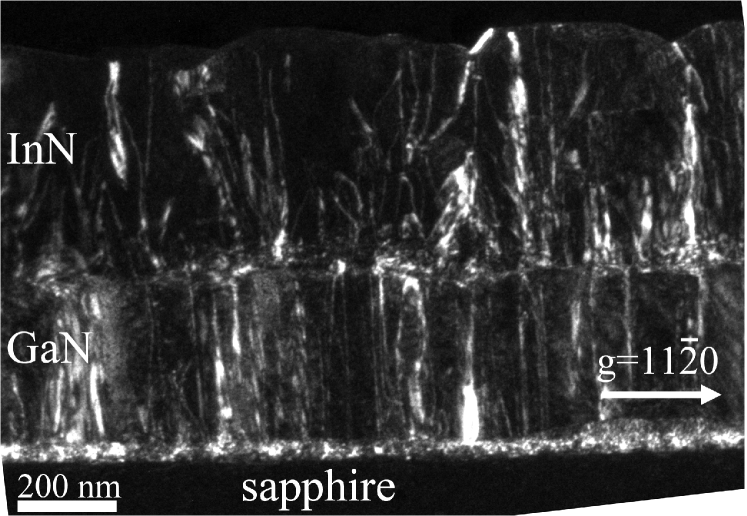
200 kV Arroyo Rojas Dasilva et al. (2010). Fig. 1 shows a TEM micrograph
obtained in weak beam (WB) conditions with g=11-20 for a
representative Si-doped sample. Edge and mixed type dislocations are
visible distributed throughout the InN layer with an average density
of cm-2 and cm-2,
respectively. An agglomeration of dislocations close to the InN/GaN
interface can be noticed. The density of screw type dislocations is
cm-2 which corresponds to 6% of the
total dislocation density. Additionally, a high density (cm-1) of stacking faults was revealed for WB
conditions Arroyo Rojas Dasilva et al. (2010) with g=10-10 (not shown here). In the
irradiated InN film, earlier TEM results Liliental-Weber
et al. (2007)
showed irradiation-induced formation dislocation loops in addition
to a significant density of planar defects introduced during growth.
After annealing at 475 ∘C the density of dislocation loops
increased from cm-2 to cm-2 Liliental-Weber
et al. (2007); Jones et al. (2007). Vacancy
agglomeration after annealing was proposed as reason for this
increase.
We applied PAS to investigate vacancy-type point defects and their
nature in the InN samples. Using a mono-energetic positron beam,
depth-dependent Doppler broadening spectra were recorded at room
temperature to probe the momentum distribution of annihilating
electron-positron pairs. Details on the experimental technique and
setup can be found elsewhere Saarinen et al. (1998); Rauch et al. (2011).
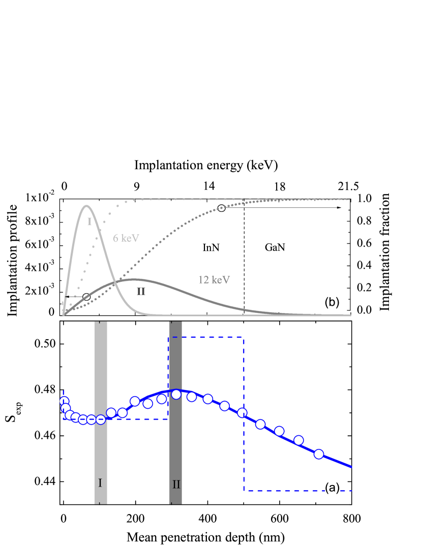
Fig. 2(a) shows the measured S-parameters of
a representative Si-doped sample for positron implantation energies
from 0-20 keV. After annihilation at surface-specific states for low
implantation energies, the S-parameter drops quickly to a local
minimum at 6 keV. Comparison with the positron implantation
profile at that energy [Fig. 2(b)] reveals
that this point is representative for annihilations from the first
150nm of the sample, with a mean implantation depth of
=100nm. Deeper inside the sample, the S-parameter increases
to a local maximum at 12 keV (corresponding to a mean
implantation depth of =310nm) and positrons probe a wide
region reaching the interface to the GaN buffer layer. For higher
implantation energies a significant amount of positrons annihilate
in the GaN buffer layer pulling the measured S-parameter towards the
value of the GaN lattice. The solid curve in
Fig. 2(a) shows a fit of the measured
spectrum using the multi-layer fitting program
VEPFIT van Veen et al. (1995). It reveals that the experimental spectrum
can be well described assuming a two-layer structure of the
S-parameter inside the InN film (see dashed line) with a 300 nm
thick near-surface and 200 nm thick near-interface layer and a
positron diffusion length of 5 nm.
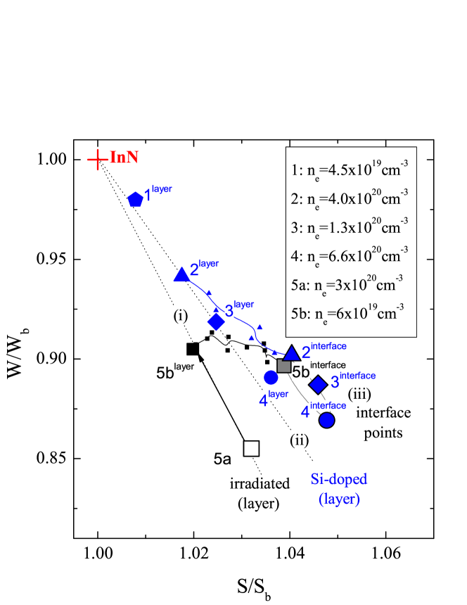
Representative for the near-surface (”layer”) and near-interface
(”interface”) areas, the measured S and W parameter at 6 and 12 keV
are plotted in Fig. 3 together with accordingly determined
values of the remaining samples. All points are normalized by the
value of an InN reference sample for which no positron trapping at
open volume defects is observed Rauch et al. (2011). Samples 1 and 5a
did not exhibit any depth-profile and therefore only one set of
parameters is displayed. For all Si-doped samples (samples 1-4), the
”layer” points fall on one line through the reference value of the
InN lattice. Hence Saarinen et al. (1998), one dominant vacancy-type
positron trap is present in this area with increasing
(room-temperature) annihilation fraction from sample 1-4. For the
”interface” points, a deviation from the ”layer” line is visible due
to increasing S-parameters and comparably less pronounced decrease
in the W-parameters. Therefore, a different dominant vacancy-type
positron trap has to be expected here. The slope defined by the
irradiated sample before annealing (sample 5a) is
steeper Tuomisto
et al. (2007a) than for the as-grown samples. Upon
rapid thermal annealing (RTA) Jones et al. (2007) (sample 5b), a
profile in the depth dependent spectrum of the S-parameter is
developed Reurings et al. (2010) with a layer and interface-specific
value. The near-surface ”layer”-point is shifted closer toward the
InN lattice point but remains on the same line as the as-irradiated
sample. This indicates a decrease in annihilation fraction at the
same positron trap as before annealing. The ”interface” point,
however, deviates strongly after annealing and is moved close to the
interface points of the Si-doped samples.
We find 3 different dominant vacancy-type positron traps in the InN
samples, i.e., defects created by high-energy particle irradiation
(i), defects dominant at the near-surface area of as-grown Si-doped
samples (ii), and defects responsible for the observed changes at
the interfaces of both Si-doped as well as RTA-treated, irradiated
samples (iii). A comparison of high-resolution coincidence Doppler
broadening spectra with density functional theory (DFT) calculations
of positron trapping and annihilation in InN
reveals Rauch et al. (2011) that these positron traps can be
identified as (i) isolated In vacancies (), (ii)
mixed In-N divacancies (-), and (iii)
bigger - () vacancy
complexes, respectively. High-energy particle irradiation introduces
isolated as dominant vacancy-type positron traps in
InN. Subsequent annealing leads to a re-arrangement of vacancy
defects Reurings et al. (2010), as observable in both TEM and positron
annihilation measurements. become mobile at or below
the annealing temperature and start to move toward the surface and
the interface with the GaN buffer, respectively, where they either
recombine, anneal out (at the surface) or form complexes with
residual (interface). Based on the employed annealing
temperature of 475∘C, we can
estimate Limpijumnong and Van de
Walle (2004) an upper limit of for the migration barrier of the . This is in
good agreement with the calculated value of 1.6 eV Duan and Stampfl (2009)
and indicates that isolated are mobile during InN
growth (assuming usual growth temperatures of C
for, e.g., MBE).
No isolated are observed in our
measurements of as-grown Si-doped InN. Instead, we find
- complexes. Hence, we conclude that
in-grown are stabilized through the formation of
complexes with . This is supported by recent DFT
results Duan and Stampfl (2009) which predict a positive binding energy
between and . Vacancy-stabilization
through the formation of vacancy-donor complexes has been observed
also in GaN (Ref. Tuomisto
et al. (2007b), and references therein) and
AlN Mäki et al. (2011). The increased incorporation of
complexes with increasing free electron concentration suggests
strongly that -related defects act as a source of
compensation in n-type InN, which is in line with theoretical
results Stampfl et al. (2000). The enhanced formation of larger
- complexes toward the interface with
the GaN buffer layer (in irradiated material after annealing as well
as Si-doped samples) indicates that the InN/GaN interface is
attractive for vacancy defects. An additional high density of
in that area could provide the proximity required for
the promotion of efficient vacancy -
clustering. However, neutral and positively charged isolated
and -complexes can not be detected in
PAS measurements Rauch et al. (2011). Duan et al. have
calculated Duan and Stampfl (2008) a positive binding energy between single
under n-type conditions and a strong tendency for the
formation of larger clusters. Hence, the formation of
- complexes could occur through a
precursor state of
-, in accordance to what has been
proposed earlier in Mg-doped InN Uedono et al. (2009).
Based on the TEM data, the observed increase in vacancy clustering
at the InN/Gan interface coincides with elevated dislocation
densities in that area. In order to assess the effect of
dislocations on the formation energies of point defects in their
vicinity we performed DFT calculations of strained InN lattices. We
found that typical strain associated with screw dislocations (0-15%
shear) decreases the formation energies of and
only slightly by 30 meV, and hence should not
play any major role. Investigations on the effects of edge
dislocations are under way. Besides strain-related influences on the
defect formation energies, additional dislocation-related vacancy
formation mechanisms such as dislocation movement and/or decoration
of dislocations might be possible. In GaN, recent theoretical
calculations Kraeusel and Hourahine (unpublished) suggest stable configurations of
vacancies inside dislocation cores and a correlation between vacancy
densities and dislocations was found Oila et al. (2003). It should be
noted that dislocations might also directly affect the positron
annihilation signal Tengborn et al. (2006) by, e.g., forming shallow
traps for positrons. The exceptionally low values of the positron
diffusion length in the InN samples do support the presence of such
additional positron trapping centers with annihilation
characteristics close to the bulk. Detailed theoretical
investigations on positron trapping and annihilation at dislocations
in wurtzite semiconductors are currently being performed.
In summary, combining results from PAS and TEM we find that isolated
are only present in irradiated InN films and anneal
out at temperatures of ∘C if not stabilized by
other point defects. Stabilization of occurs through
complex formation with .
- complexes are the dominant
vacancy-type positron trap in as-grown InN samples. Toward the
interface between the InN layer and the GaN buffer, enhanced
formation of bigger vacancy clusters with increasing number of
is observed in both as-grown and irradiated material
after annealing and coincides with increased dislocation densities
in that area. This indicates that the InN/GaN interface is strongly
attractive for vacancy defects and points at elevated concentrations
of additional and
-complexes in that area.
The authors wish to thank T. Veal for helpful discussions. This work
has been supported by the European Commission under the 7th
Framework Program through the Marie Curie Initial Training Network
RAINBOW, Contract No. PITN-Ga-2008-213238, and the Academy of
Finland.
References
- King et al. (2008) P. D. C. King, T. D. Veal, P. H. Jefferson, S. A. Hatfield, L. F. J. Piper, C. F. McConville, F. Fuchs, J. Furthmüller, F. Bechstedt, H. Lu, et al., Phys. Rev. B 77, 045316 (2008).
- Monemar (1999) B. Monemar, J. Mater. Sci. Mater. Electron. 10, 227 (1999).
- Janotti and de Walle (2008) A. Janotti and C. G. Van de Walle, 92, 032104 (2008).
- Stampfl et al. (2000) C. Stampfl, C. G. Van de Walle, D. Vogel, P. Krüger, and J. Pollmann, Phys. Rev. B 61, R7846 (2000).
- Piper et al. (2006) L. F. J. Piper, T. D. Veal, C. F. McConville, H. Lu, and W. J. Schaff, Appl. Phys. Lett. 88, 252109 (2006).
- Jones et al. (2007) R. E. Jones, S. X. Li, E. E. Haller, H. C. M. van Genuchten, K. M. Yu, J. W. Ager III, Z. Liliental-Weber, W. Walukiewicz, H. Lu, et al., Appl. Phys. Lett. 90, 162103 (2007).
- Schaff et al. (2004) W. J. Schaff, H. Lu, L. F. Eastman, W. Walukiewicz, K. M. Yu, S. Keller, S. Kurtz, B. Keyes, and L. Gevilas, in State-of-the-Art Program on Compound Semiconductors XLI and Nitride and Wide Bandgap Semiconductors for Sensors, Photonics, and Electronics V, edited by H. M. Ng and A. G. Baca (Electrochemical Society, Honolulu, HI, 2004), vol. 2004-06 of The Electrochemical Society Proceedings Series, p. 358.
- Arroyo Rojas Dasilva et al. (2010) Y. Arroyo Rojas Dasilva, M. P. Chauvat, P. Ruterana, L. Lahourcade, E. Monroy, and G. Nataf, J. Phys. Cond. Matt. 22, 355802 (2010).
- Liliental-Weber et al. (2007) Z. Liliental-Weber, R. Jones, H. van Genuchten, K. Yu, W. Walukiewicz, J. W. Ager III, E. Haller, H. Lu, and W. Schaff, Physica B 401-402, 646 (2007).
- Saarinen et al. (1998) K. Saarinen, P. Hautojärvi, and C. Corbel, Positron Annihilation Spectroscopy of Defects in Semiconductors, vol. 51A of Semiconductors and Semimetals (Academic Press, New York, 1998).
- Rauch et al. (2011) C. Rauch, I. Makkonen, and F. Tuomisto, Phys. Rev. B 84, 125201 (2011).
- van Veen et al. (1995) A. van Veen, H. Schut, M. Clement, J. M. M. de Nijs, A. Kruseman, and M. R. IJpma, Appl. Surf. Sci. 85, 216 (1995).
- Tuomisto et al. (2007a) F. Tuomisto, A. Pelli, K. M. Yu, W. Walukiewicz, and W. J. Schaff, Phys. Rev. B 75, 193201 (2007a).
- Reurings et al. (2010) F. Reurings, C. Rauch, F. Tuomisto, R. E. Jones, K. M. Yu, W. Walukiewicz, and W. J. Schaff, Phys. Rev. B 82, 153202 (2010).
- Limpijumnong and Van de Walle (2004) S. Limpijumnong and C. G. Van de Walle, Phys. Rev. B 69, 035207 (2004).
- Duan and Stampfl (2009) X. M. Duan and C. Stampfl, Phys. Rev. B 79, 174202 (2009).
- Tuomisto et al. (2007b) F. Tuomisto, T. Paskova, R. Kroger, S. Figge, D. Hommel, B. Monemar, and R. Kersting, Appl. Phys. Lett. 90, 121915 (2007b).
- Mäki et al. (2011) J.-M. Mäki, I. Makkonen, F. Tuomisto, A. Karjalainen, S. Suihkonen, J. Räisänen, T. Y. Chemekova, and Y. N. Makarov, Phys. Rev. B 84, 081204 (2011).
- Duan and Stampfl (2008) X. M. Duan and C. Stampfl, Phys. Rev. B 77, 115207 (2008).
- Uedono et al. (2009) A. Uedono, H. Nakamori, K. Narita, J. Suzuki, X. Wang, S. B. Che, Y. Ishitani, A. Yoshikawa, and S. Ishibashi, J. Appl. Phys. 105, 054507 (2009).
- Kraeusel and Hourahine (unpublished) S. Kraeusel and B. Hourahine Phys. Status Solidi A DOI:10.1002/pssa.201100097 (2011).
- Oila et al. (2003) J. Oila, J. Kivioja, V. Ranki, K. Saarinen, D. C. Look, R. J. Molnar, S. S. Park, S. K. Lee, and J. Y. Han, Appl. Phys. Lett. 82, 3433 (2003).
- Tengborn et al. (2006) E. Tengborn, M. Rummukainen, F. Tuomisto, K. Saarinen, M. Rudzinski, P. R. Hageman, P. K. Larsen, and A. Nordlund, Appl. Phys. Lett. 89, 091905 (2006).