Magnetic field dependence of Pauli spin blockade: a window into the sources of spin relaxation in silicon quantum dots
Abstract
We investigate spin relaxation in a silicon double quantum dot via leakage current through Pauli blockade as a function of interdot detuning and magnetic field. A dip in leakage current as a function of magnetic field on a mT field scale is attributed to spin-orbit mediated spin relaxation. On a larger ( mT) field scale, a peak in leakage current is seen in some, but not all, Pauli-blocked transitions, and is attributed to spin-flip cotunneling. Both dip and peak structure show good agreement between theory and experiment.
Electron spins confined in semiconductor quantum dots (QDs) are attractive candidates for quantum information processing Loss and DiVincenzo (1998). Coherent manipulation of individual and coupled electron spin states has been mainly investigated in GaAs-based double QD (DQD) devices Koppens et al. (2006); Petta et al. (2005); Pioro-Ladriere et al. (2008). However, nuclear spins of the host material cause decoherence of the electron spin via strong hyperfine coupling Khaetskii et al. (2002). To reduce this effect, group IV materials, such as carbon, silicon (Si), and silicon-germanium (SiGe), have been investigated Churchill et al. (2009a); Lim et al. (2009); Xiao et al. (2010); Hu et al. (2007); Simmons et al. (2011) because their most abundant isotopes have zero nuclear spin. Silicon systems, in particular, have an advantage for future integration because of their compatibility with conventional Si metal-oxide-semiconductor devices.
Toward spin qubits in Si systems, it is necessary to understand the spin relaxation mechanism. Pauli spin blockade (PSB) Ono et al. (2002); Johnson et al. (2005) is a valuable tool for investigating spin relaxation in confined systems. In DQDs of several materials, the spin relaxation mechanism has been characterized by analyzing the leakage current in the PSB regime Koppens et al. (2005); Pfund et al. (2007); Churchill et al. (2009b); Kodera et al. (2009), where hyperfine interaction and/or spin-orbit interaction dominate the spin relaxation. For Si systems, a PSB has been reported for a DQD in metal-semiconductor-oxide structures and an electrostatically formed DQD in Si/SiGe heterostructures Shaji et al. (2008); Liu et al. (2008). However, the relaxation mechanism in Si DQDs has not yet been experimentally clarified. More recently, magnetic field dependences of the leakage current in a PSB regime have been demonstrated in a pure Si DQD Lai et al. (2010), where a current peak was explained by field-dependent cotunneling.
In this Letter, we investigate leakage current in a PSB regime using a lithographically defined Si DQD. By changing magnetic field, we observed a dip of the leakage current at zero magnetic field, presumably the result of spin-orbit-mediated spin relaxation. In addition, magnetic field dependences at a different charge triple point exhibit a leakage current peak at zero magnetic field. This peak can be understood as a signature of spin-flip cotunneling processes.
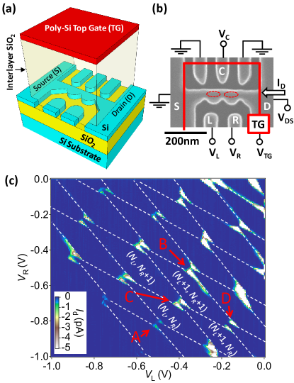
Figure 1(a) shows a schematic of a Si DQD. Three constrictions between the source (S) and drain (D), and five side gates were patterned by electron beam lithography on a 60-nm-thick (100) Si-on-insulator (SOI) layer, where the thickness of the buried oxide was 400 nm. Reactive ion etching was used to transfer the resist pattern onto the SOI, followed by formation of the gate oxide via thermal oxidation for 30 min at 1000 ℃ and low-pressure chemical vapor deposition (LPCVD). Then, a wide poly-Si top gate (TG) formed by LPCVD was used as an ion implantation mask for the formation of the n-type S and D regions. Finally, 300-nm-thick aluminum contact pads were formed by electron beam evaporation. Figure 1(b) shows a scanning electron microscope image of the device, where the DQD is defined by tunnel barriers at the three constricted regions Yamahata et al. (2009).
Electrons were attracted to the Si (100) surface by applying a positive TG voltage, . Electrochemical potentials of the left and right QDs were modulated by applying voltages and to side gates L and R. The tunnel coupling between the two QDs was controlled by voltage applied to side gate C. All measurements were carried out in a 3He refrigerator with a base temperature of 250 mK.
The honeycomb charge stability [Fig. 1(c)] reflects the formation of a DQD van der Wiel et al. (2003). Charging energies of the left and right QDs were estimated to be and meV, respectively, from the spacings of the Coulomb peaks, implying that the QDs have almost the same size. In addition, from the distribution of the current peaks due to resonant tunneling at triple point A in Fig. 1(c), the quantum level spacing, , of the left and right QD was estimated to be 310 and 260 eV, respectively EPA . In confirmation, can be approximated as , where gives effective mass here, is Planck’s constant, and is the area of the QD Kouwenhoven et al. (1997), with spin and valley degeneracies included. This equation determines to be between 260 and 380 eV for our device geometry EPA , in good agreement with the experimental estimation. We conclude that the QD is formed between the two constricted regions indicated by the ovals in Fig. 1(b).
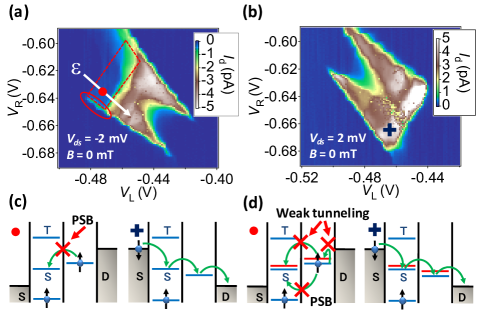
Current rectification in DQDs due to a PSB appears at a triple point with only one bias polarity Johnson et al. (2005). We observed such current rectification with a negative bias voltage at triple point B in Fig. 1(c), as indicated by the trapezoid in Fig. 2(a), whereas no current rectification appeared with positive bias as shown in Fig. 2(b). In addition, the current rectification is lifted along the outer edge of the PSB regime indicated by the circle in Fig. 2(a) because of electron exchanges between the DQD and the right lead, comparable to PSB seen in GaAs DQDs Johnson et al. (2005).
Since Si DQDs normally have doubly degenerate valleys due to confinement in the direction perpendicular to the Si surface, the valley degeneracy could lift a PSB. However, the fact that a PSB is observed indicates either a lifting of valley degeneracy or weak tunneling between valleys Culcer et al. (2010). In the former case, once two spins occupy the (1, 1) triplet state as shown in Fig. 2(c), the current flow is suppressed due to the PSB until relaxation from (1, 1) triplet to (1, 1) singlet occurs. In the latter case, even if degenerate valleys exist as shown in Fig. 2(d), the PSB is not lifted because intra-dot and inter-dot tunnelings between valleys are weak.
PSB features were observed at adjacent triple points, marked B, C, and D in Fig. 1(c). This is not expected for simple spin- PSB. Since the DQD has many electrons, spin- ground states can exist, leading to scenarios for consecutive PSB Johnson et al. (2005). Blockade where valley degeneracy plays a role can also lead to consecutive PSB-like features. Even when a spin doublet is formed in DQDs, the current flow could be suppressed because of weak tunneling between valleys discussed above EPA .
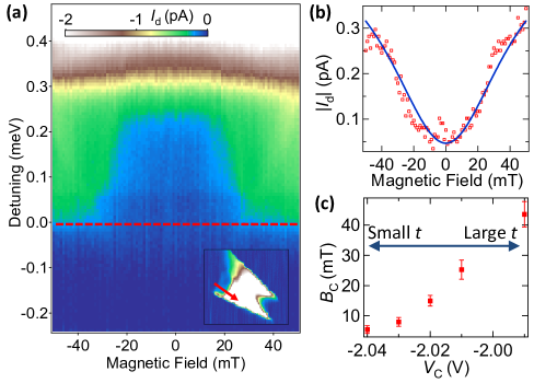
Figure 3(a) shows the leakage current in the PSB regime at triple point C in Fig. 1(c) as a function of magnetic field applied normally to the DQD with a detuning, , corresponding to the arrow shown in the inset. A strong current dip was observed at , whereas the current with opposite bias does not change as a function of magnetic fields EPA . Similar current dips have been observed for DQDs in InAs nanowires Pfund et al. (2007); Nadj-Perge et al. (2010) and carbon nanotubes Churchill et al. (2009b) and can be attributed to spin-orbit induced relaxation Danon and Nazarov (2009), which is suppressed at due to a Van Vleck cancellation Pfund et al. (2007); Khaetskii and Nazarov (2001). A Lorentzian line shape, with characteristic width , is predicted theoretically Danon and Nazarov (2009). The squares in Fig. 3(b) correspond to the absolute values of the leakage current in the PSB regime along the dashed line in Fig. 3(a). Fits to the Lorentzian form (the blue curve in Fig. 3(b)) yield good agreement between theory and experiment. Furthermore, as the inter-dot tunneling between the two QDs is enhanced by changing , the value of extracted from the fit increases, as plotted in Fig. 3(c). This result is also consistent with the theory, which predicts proportional to inter-dot tunnel coupling Danon and Nazarov (2009). These results suggest that spin-orbit effects dominate spin relaxation in these devices.
Another possible mechanism leading to a dip in current leakage around is spin-valley blockade with short-range disorder Pályi and Burkard (2010), where the current dip as a function of magnetic-field-induced valley splitting is predicted. However, we have no independent evidence that the required B-dependent valley splitting exists. The physics of the valley in Si DQDs deserves further experimental and theoretical study.
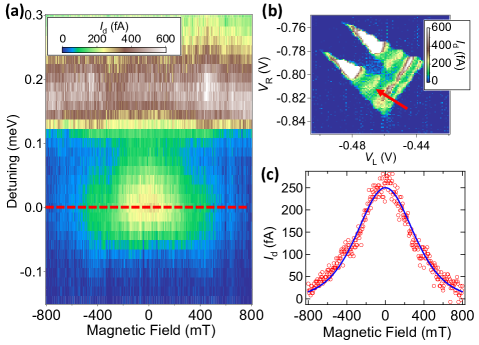
For some triple points, we observe a peak, rather than dip, in PSB leakage current on a larger field scale. As an example, the field dependence of the leakage current at triple point A in Fig. 1(c) is shown in Fig. 4(a). The arrow in the magnified plot of triple point A shown in Fig. 4(b) corresponds to the detuning axis in Fig. 4(a). Among the 15 triple points that show PSB [Fig. 1(c)], nine show a zero-field current dip and two show a peak. We also observed current peaks outside a current dip in some cases.
In GaAs DQDs, zero-field peaks in leakage current were attributed to hyperfine-induced spin relaxation Koppens et al. (2005); Jouravlev and Nazarov (2006). However, the contribution of the hyperfine interaction should be small in Si systems, because the dominant 28Si atoms have zero nuclear spin. Using 4.7 % natural abundance of 29Si and lithographic device dimensions EPA gives an expected number of nuclear spins in a Si DQD to be - , corresponding to a fluctuating Overhauser field magnitude - T, where the hyperfine coupling constant eV from NMR measurements Shulman and Wyluda (1956) and for electrons in Si. Since the peak width in Fig. 4(c) is larger than by a factor of 104, the mechanism of the current peaks at is not explained by hyperfine interaction.
Similar peaks were also seen in Si DQD in Ref. Lai et al. (2010), where the peak is well described by spin-flip cotunneling Coish and Qassemi (2011). When ( is Boltzmann’s constant and is the inter-dot tunnel coupling), the spin-flip cotunneling current is given by with where is the coupling of the lead to the left (right) dot, is the depth of the two-electron level Qassemi et al. (2009), and is inter-dot charging energy. Since we observed clear resonant tunneling peaks, is larger than Fujisawa et al. (1998). In addition, if , the current would be much larger than the observed current shown in Fig. 4(b). As a result, so that can be used to fit the current peak. The blue curve in Fig. 4(c) is , which has a good agreement with the data by using , yielding and . Since the current does not vary much along the base of the triangle in Fig. 4(b), we assume . By using expression of with , , , and estimated from the bias triangle shown in Fig. 4(b), we extracted eV. Furthermore, can be extracted to be about eV from the unblocked resonant tunneling peak current () with Eq. (15) in Ref. van der Wiel et al. (2003). These values are similar with those in Ref. Lai et al. (2010) and in an experimentally reasonable range so that the spin-flip cotunneling processes are most likely the mechanism of the peak. It should be noted that, as for the dip in Fig. 3, spin-valley blockade with disorder could also explain the peak, but again we have at present no evidence of the required field-dependent valley splitting Burkard and Pályi .
Acknowledgements.
GY and TK contributed equally to this work. We thank W. A. Coish, G. Burkard, A. Pályi, C. Barthel, J. Medford, and F. Kuemmeth for valuable discussions and K. Usami, T. Kambara, R. Suzuki, and T. Hiramoto for device fabrication. This work was partly supported by a Grant-in-Aid for Scientific Research from the Ministry of Education, Culture, Sports, Science, and Technology of Japan (No. 21710137, No. 19206035, and No. 22246040), JST-PRESTO, and Special Coordination Funds for Promoting Science and Technology.References
- Loss and DiVincenzo (1998) D. Loss and D. P. DiVincenzo, Phys. Rev. A 57, 120 (1998).
- Koppens et al. (2006) F. H. L. Koppens, et al., Nature 442, 766 (2006).
- Petta et al. (2005) J. R. Petta et al., Science 309, 2180 (2005).
- Pioro-Ladriere et al. (2008) M. Pioro-Ladriere, et al., Nat. Phys. 4, 776 (2008).
- Khaetskii et al. (2002) A. V. Khaetskii, D. Loss, and L. Glazman, Phys. Rev. Lett. 88, 186802 (2002).
- Churchill et al. (2009a) H. O. H. Churchill, et al., Phys. Rev. Lett. 102, 166802 (2009a).
- Lim et al. (2009) W. H. Lim, et al., Appl. Phys. Lett. 94, 173502 (2009).
- Xiao et al. (2010) M. Xiao, M. G. House, and H. W. Jiang, Phys. Rev. Lett. 104, 096801 (2010).
- Hu et al. (2007) Y. Hu, et al., Nat. Nanotechnol. 2, 622 (2007).
- Simmons et al. (2011) C. B. Simmons, et al., Phys. Rev. Lett. 106, 156804 (2011).
- Ono et al. (2002) K. Ono, D. G. Austing, Y. Tokura, and S. Tarucha, Science 297, 1313 (2002).
- Johnson et al. (2005) A. C. Johnson, et al., Phys. Rev. B 72, 165308 (2005).
- Koppens et al. (2005) F. H. L. Koppens, et al., Science 309, 1346 (2005).
- Pfund et al. (2007) A. Pfund, I. Shorubalko, K. Ensslin, and R. Leturcq, Phys. Rev. Lett. 99, 036801 (2007).
- Churchill et al. (2009b) H. O. H. Churchill, et al., Nat. Phys. 5, 321 (2009b).
- Kodera et al. (2009) T. Kodera, et al., Phys. Rev. Lett. 102, 146802 (2009).
- Shaji et al. (2008) N. Shaji, et al., Nat. Phys. 4, 540 (2008).
- Liu et al. (2008) H. W. Liu, et al., Phys. Rev. B 77, 073310 (2008).
- Lai et al. (2010) N. S. Lai, et al., Scientific Reports 1, 110 (2011).
- Yamahata et al. (2009) G. Yamahata, et al., Appl. Phys. Express 2, 095002 (2009).
- van der Wiel et al. (2003) W. G. van der Wiel, et al., Rev. Mod. Phys 75, 1 (2003).
- (22) See http://marcuslab.harvard.edu/SiDQDsupp.pdf for supplementary information.
- Kouwenhoven et al. (1997) L. P. Kouwenhoven, et al., Mesoscopic Electron Transport (Springer, 1997), vol. 345 of NATO Science Series E, pp. 105–214.
- Culcer et al. (2010) D. Culcer, Ł. Cywiński, Q. Li, X. Hu, and S. D. Sarma, Phys. Rev. B 82, 155312 (2010).
- Nadj-Perge et al. (2010) S. Nadj-Perge, et al., Phys. Rev. B 81, 201305(R) (2010).
- Danon and Nazarov (2009) J. Danon and Y. V. Nazarov, Phys. Rev. B 80, 041301(R) (2009).
- Khaetskii and Nazarov (2001) A. V. Khaetskii and Y. V. Nazarov, Phys. Rev. B 64, 125316 (2001).
- Pályi and Burkard (2010) A. Pályi and G. Burkard, Phys. Rev. B 82, 155424 (2010).
- Jouravlev and Nazarov (2006) O. N. Jouravlev and Y. V. Nazarov, Phys. Rev. Lett. 96, 176804 (2006).
- Schliemann et al. (2003) J. Schliemann, A. Khaetskii, and D. Loss, J. Phys.: Condens. Matter 15, R1809 (2003).
- Shulman and Wyluda (1956) R. G. Shulman and B. J. Wyluda, Phys. Rev. 103, 1127 (1956).
- Coish and Qassemi (2011) W. A. Coish and F. Qassemi, arXiv:1109.4445 (2011).
- Qassemi et al. (2009) F. Qassemi, W. A. Coish, and F. K. Wilhelm, Phys. Rev. Lett. 102, 176806 (2009).
- Fujisawa et al. (1998) T. Fujisawa, et al., Science 282, 932 (1998).
- (35) G. Burkard and A. Pályi, private communication.