e-mail: sworakowski@pwr.wroc.pl††thanks: Wyb. Wyspianskiego 27, 50-370 Wrocław, Poland\sanitize@url\@emaile-mail: sworakowski@pwr.wroc.pl††thanks: Prosp. Nauky 46, 03680 Kyiv, Ukraine
Bistable organic materials in optoelectrical switches: Two-electrode devices vs organic field effect transistors
Abstract
We present a short overview of research into properties of organic materials and structures that could be used in optoelectrical switches, i.e., switches in which changes in electrical properties are triggered by light of appropriate wavelengths. In particular, we describe the structures acting by virtue of reversible photochemical reactions occurring in photochromic molecular materials.
1 Introduction
One of the topics extensively studied in the domain of organic electronics and photonics is the design and the fabrication of structures that could serve as elements of memories and switches. According to the textbook definition, a switch is a mechanical, electrical, electronic, or optical device for opening or closing a circuit, or for diverting the energy or charge from one part of a circuit to another.
Figure 1 shows schematically the principle of action of a switch: the structure, in its state ‘‘1’’ characterized by certain optical, electrical, magnetic or mechanical parameters and stable for a certain time interval, is converted by an activating stimulus to state ‘‘2’’ (stable or metastable) characterized by another set of parameters. The structure reverts to its initial state by a deactivating stimulus. It is the matter of course that the hearts of such structures should contain a multistable element. The activating and deactivating stimuli can be optical, electrical, or magnetic (e.g., the illumination with radiation triggering a chemical reaction, electrical pulse switching the polarization of a ferroelectric dielectric, pulse of a magnetic field switching the magnetization, etc.
The recent paper by Heremans et al. [1] provides an extensive review of electrically programmable memory devices. In this paper, we present a short overview of research into properties of organic materials and structures that could be used in optoelectrical switches, i.e., switches in which changes in electrical properties would be triggered by light of appropriate wavelengths. In particular, we will concentrate on structures acting by virtue of reversible photochemical reactions occurring in photochromic molecular materials.
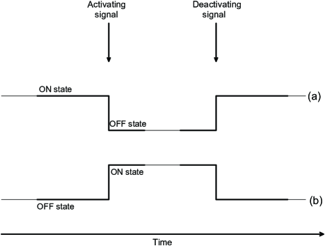
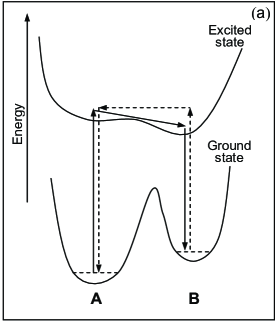
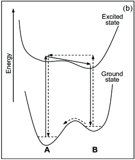
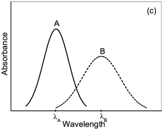
The photochromic molecules are good examples of optically driven bistable systems [2] that may allow one to control the current by the illumination with light activating a reversible photochemical reaction. The light of a given wavelength triggers the reaction by changing electronic properties of a molecule (energies of electronic levels, charge distribution on the molecule, etc.), while an exposure to the radiation of a different wavelength results in a reverse reaction, resulting in the return of the system to its initial state (cf. Fig. 2). Suitably selected thermally stable photochromic molecules are able to remain in their metastable form for a sufficiently long time; hence, the current does not drop down after turning off the illumination. The performance of the switch is determined by the ratio of high-current (on) and low-current (off) states (Fig. 1).
2 Two-electrode Structures
2.1 Photochromic moieties molecularly dispersed in organic semiconductor
The idea of light-triggered electrical switching has been put forward as early as a decade ago [3–6]. Early experiments carried out on two-electrode structures (in sandwich or surface arrangement) [7–11] contained photochromic systems and - or -conjugated semiconducting polymers.
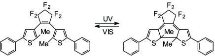
Conceptually, the simplest way to achieve the effect is to graft a suitable photochromic unit into the chain of a conjugated polymer. This idea was developed by Kawai et al. [11] who incorporated photochromic diarylethene directly into the main chain of a semiconducting polymer (Fig. 3). The stable form of diarylethene lacks the conjugation between the two moieties. Hence, the mean free path of charge carriers should not exceed the average distance between the incorporated photochromic groups. The conjugation path opens under UV illumination, resulting in an increase of the mean free path. Thus, electrically, with the stable form in the chain, the system is in the ‘‘OFF’’ state, the UV illumination switches it to the ‘‘ON’’ state, and the illumination with visible light, triggering the reverse photochromic reaction, switches the molecule back to the ‘‘OFF’’ state.
The system put forward by Sworakowski, Nešpurek, and coworkers [3–8] also made use of a single-phase two-electrode system comprising a conjugated polymer matrix and photochromic molecules, either dissolved in the matrix or chemically attached to the polymer chain as side groups (Fig. 4). The transport of charge carriers on chains of a semiconducting polymer can be modulated by traps created and annihilated by photochemically transformed photochromic molecules. The mechanisms of trap formation slightly differ for electron and hole transports [12]. As most organic semiconductors are of the -type, we will limit our discussion to the formation of traps for holes.
One may envisage the formation of two types of traps by photochromic groups attached to polymer chains or by photochromic molecules dissolved in organic semiconducting (polymeric or low molecular weight) matrices: chemical traps and dipolar traps. If the ionization energy of a photochromic species is lower than that of the matrix, then chemical traps for holes are formed on the photochromic dopant. The depth of such traps depends on the difference of the ionization energies of the matrix ( and the dopant (. Neglecting the second-order effects, the depth of a chemical trap may be written as [12]
| (1) |
where the superscript indicates the ionization energy of an isolated molecule. The dipolar traps [13-16] are formed on molecules in a vicinity of the dopant, if the dopant molecule is polar (i.e., possesses a non-zero permanent dipole moment), and the matrix is either non-polar or weakly polar. In this case, the trap depth is approximately equal to the interaction energy of the dipole moment of the dopant and the carrier situated on an adjacent molecule of the matrix. In the simplest case of a non-polar isotropic matrix, the approximate expression reads
| (2) |
where is the unit charge, stands for the dipole moment of the dopant, is the relative electric permittivity of the matrix, is the distance between the charge and the dipolar dopant, and is the angle between the dipole moment and the radius vector of . The trap depth is thus proportional to the dipole moment of the dopant. More exact calculations performed on a model molecular system [14, 15] showed that traps as deep as ca. 0.6–0.7 eV can be created on a molecule adjacent to a dipole (0.6 nm apart) whose electrical moment amounts to 12 D. Experiments performed mainly of -conjugated polymer poly[(methylphenyl)silane] containing photochromic spiropyran (Fig. 4) evidenced the opto-electrical switching; the performance of two-electrode structures appeared, however, moderate [7, 8]. As it seems, the unsatisfactory performance of the switches results from important limitations that must be overcome in practical realization. First of all, certain relations between energy levels of the matrix and the photochromic moieties have to be fulfilled [17]:
i) in order to prevent the simultaneous excitation of the matrix and photochromic molecules, their excitation energies should be separated (;
ii) in order to prevent the energy transfer from the excited state of photochromic molecules to the matrix, the energy of the excited state of the matrix (measured with respect to a common external reference) should be higher that that of the photochrom, i.e., the following condition should be fulfilled:
| (3) |
Moreover, a good performance of the device may only be achieved if other important requirements are met:
iii) good chemical stability even in the short-wavelength part of the spectrum (it would be better to realize the excitation with light of low photon energy);
a
b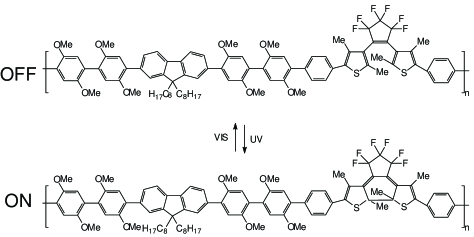
c
a
b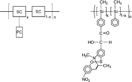
c
iv) fast photochemical reaction with small conformational changes of photochromic molecules – large changes of a molecular conformation make the photochromic reaction slow;
v) the matrix must have free volume enabling conformational changes of the photochromic moieties;
vi) in the case of a binary system consisting of a photochromic additive dissolved in a polymer or low-molecular weight matrix, the mutual miscibility must be sufficiently high;
vii) in order to prevent the uncontrolled thermal reverse reaction, the ground-state energy barrier between two forms of the photochromic system must be sufficiently high;
viii) the difference of dipole moments and/or ionization energies of both forms should be as large as possible.
It must be realized that the simultaneous fulfilment of all these conditions can be quite difficult. Thus, the practical realization of a technologically useful single-phase two-electrode optoelectrical switch is a task that requires much effort, in particular from materials scientists and synthetic chemists.
2.2 Photochromic film on the surface of an organic semiconductor
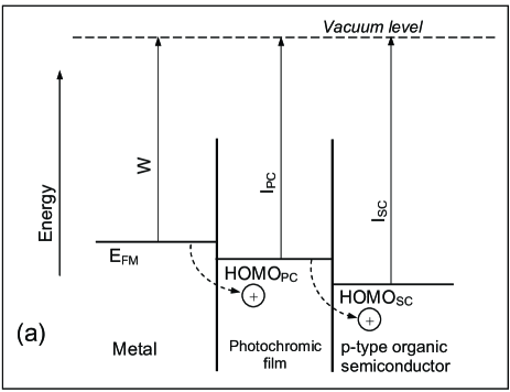
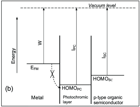
A different approach was proposed by Jakobsson et al. [18]. In their structure (Fig. 5), the photochromic material was placed between an organic semiconductor and a metal; the photochromic reaction resulted in the reversible change of a barrier for the injection of charge carriers, by reversibly modifying the current. Considering a -type semiconductor, the basic parameter is the relation between energies of the HOMO levels (ionization energies if measured with respect to the vacuum level) of stable and metastable forms of the photochromic system and the work function of the metal electrode. In some materials, the ionization energies of two states of the photochromic moieties are quite different (as, for example, is the case of diarylethene and spiropyran). A change of the ionization energy modifies the energy difference between HOMO of the photochromic material and the Fermi level of an electrode, resulting in a change of the injection barrier for holes and, hence, the current flow through the structure [18].
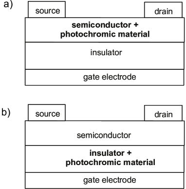
3 Photoswitchable Organic Field Effect Transistors
Organic field effect transistor (OFET) is a three-electrode structure (cf. Fig. 6), in which the current flowing in a semiconductor between two active electrodes (‘‘source’’ and ‘‘drain’’) can be modified by a voltage applied to the third electrode (’’gate’’) separated from the semiconductor by an insulating film [19]. In general, the source-drain current, , is therefore a function of the source-drain voltage, , and gate voltage, . The expressions describing the current-voltage characteristics read
| (4) |
| (5) |
Equation (4) describes the course of the characteristics for low (‘‘linear range’’), whereas Eq. (5) is valid at high (‘‘saturation range’’). In the above equations, is the mobility of charge carriers, is the threshold voltage, is the insulator capacitance, and and stand for the channel length and the width, respectively.
In these structures, the photoswitchable molecules can be placed either in the semiconductor or in the insulator. Experiments with structures in the former architecture (Fig. 6,a) yielded results resembling those obtained with similar systems in the two-electrode arrangement [20]. The result can be easily rationalized: the switching is expected to affect the mobility of charge carriers in the same way as in the two-electrode structures. Thus, the processes responsible for the switching, its reversibility, its rate etc. are very much the same in the materials under study irrespective of the experimental geometry.
3.1 Photochromic species in the OFET insulator
An alternative to the architecture discussed above would be the use of a photoswitchable insulator (Fig. 6,b). This can be realized by either using a photoactive insulator (e.g., an insulating polymer with photochromic pendant groups) or by dissolving photochromic molecules in a neutral insulator. The mechanism(s) responsible for the process will be discussed below.
The structures depicted in Fig. 6,b were studied by Shen et al. [21] and, independently, by Lutsyk et al. [22, 23]. The former group reported on a reversible switching in an OFET containing -type organic semiconductor pentacene, and poly(methyl methacrylate) (PMMA) containing dissolved photochromic spiropyran (Fig. 4,a), acting as photoswitchable gate insulator. The switching was also reported in an OFET containing -type organic semiconductor perfluorinated Cu phthalocyanine [21]. The authors attributed the effect to a reversible change of the electric permittivity.
a
b
c
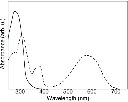
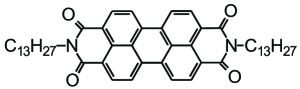
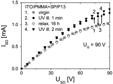
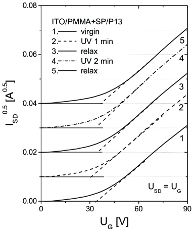
Lutsyk et al. [22, 23] studied the photoswitching in the structure consisting of an -type organic semiconductor tridecyl-substituted bis-perylenediimide (hereafter referred to as P13 – see Fig. 7,a) and PMMA containing dissolved spiropyran. The results, shown in Fig. 7, demonstrate the effective switching triggered by light. The photoswitching ratio was found dependent on the gate voltage amounting to ca. 7–8 at the lowest voltages and decreasing to ca. 1.3 at the highest voltages.
Two processes can account for the light-induced reversible modulation of the current in the structures under consideration:
i) reversible change in the capacitance of the insulator;
ii) reversible modification of the insulator-semiconductor interface.
Both processes stem from a reversible change of the dipole moment of photochromic species (admixed molecules or side groups chemically attached to the polymer chain) located either in the bulk of the insulator or at the semiconductor-insulator interface.
3.1.1. Photochromic dipoles at the
insulator-semiconductor interface
The importance of switchable polar species located on the surface of an organic semiconductor has been discussed in several publications. Shen et al. [24] deposited photochromic spiropyran molecules on the surface of -type and -type semiconductors in OFET. In -type transistors, an increase of the source-drain current after the UV illumination and a decrease of the current after visible light SP was observed, whereas the opposite effect was detected in -type devices: the current decreased after the UV illumination and rose after the exposure to visible light. The effect has been explained by assuming the contribution of a local (negative) gate voltage yielded by the dipoles created upon irradiation, resulting in an increase of the current in -type devices, and to a decrease of the current in -type OFETs. Spiropyran grafted to single-walled carbon nanotubes in transistors also showed the photoswitching effect [25]: the current dropped after the UV illumination. The phenomenon has been explained by the creation of dipole traps for charge carriers by highly polar photomerocyanine molecules produced by the photochromic reaction. However, spiropyran grafted to polyaniline chains showed the opposite photoswitching behavior: an increase of the current under the UV irradiation. The effect has been explained assuming the contribution from a local field, complementary to the gate field, appearing due to the creation of a highly polar form of the photochromic system [26].
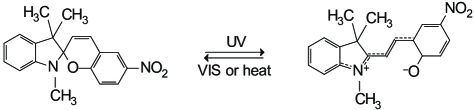
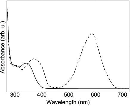
Recent reports on the reversible switching of the current in an OFET containing PMMA insulator doped with spiropyran also pointed to the effect of photochromic molecules located at the interface [22, 23]. Due to a strong interaction of interface dipoles with charge carriers in the channel (Eq. 2), interfacial charged states can be formed. A fraction of photochromic molecules dispersed in the insulator situated at the insulator–semiconductor interface creates local states on adjacent semiconductor molecules [15, 24]. The semiconductor molecules situated in a vicinity of suitably oriented dipoles (i.e., those for which ) will act as dipolar traps [15]. The remaining ones may only scatter the approaching carriers. In the first approximation, the depth of a dipolar trap will be equal to the charge-dipole interaction energy, i.e., will be described by Eq. (2). Let us consider an example: photochromic spiropyran (Fig. 4,a) admixed to PMMA. In its stable form, spiropyran (SP) has the dipole moment of ca 5.4 D. The illumination with UV light converts the stable form into metastable photomerocyanine (MR) having the dipole moment of ca. 11 D [6]. Taking the distance from the interfacial dipoles to the first molecular layer of the semiconductor equal to ca. 0.35 nm, the maximum depth of dipolar traps, given by Eq. (2) with , estimated for SP dipoles is not higher than 0.35 eV, increasing to ca. 0.7 eV after the conversion of SP to merocyanine by the UV illumination.
Changes in the parameters characterizing the interface traps affect the threshold voltage (. The threshold voltage is related to the parameters of the semiconductor and the insulator by the equation [19]
| (6) |
where stands for the surface potential of the semiconductor, is a potential supplied by the floating gate, and is a sum of the space charge in the semiconductor and a charge accumulated in the interface states. Consequently, one may expect changes in due to surface potentials and charges and the bulk capacitance. It comes from the above equation that an increase in the depth and/or density of traps should result in an increase in and/or , and in an increase in . The bulk effect will be tackled in the subsequent section.
The presence of the interface traps affects also the shapes of the current-voltage characteristics in the subthreshold region (i.e., for [19]. The current-voltage dependences in the subthreshold range of voltages are usually characterized by the subthreshold swing describing the slope of the characteristics:
| (7) |
According to [19], the latter parameter is given by the equation
| (8) |
where is the capacitance of the depletion layer of the semiconductor, is the capacitance of the insulator, and is the capacitance associated with the interface traps. It comes from Eq. (8) that, at 300 K, the lowest available value of amounts to ca. 60 mV/decade; the experimentally obtained values of the parameter are usually higher by a half to one order of magnitude. Two parameters appearing in Eq. (8), and can be reversibly modified by the photochromic reaction, thus influencing the slope of the current–voltage characteristics. The conclusion finds a support in the results of calculations published by Scheinert et al. [27] who performed simulations of the I-V characteristics in an OFET showing that the introduction of traps at the semiconductor-insulator interface results in an increase of the current in the subthreshold region and practically does not affect the current at . The increase of the subthreshold current was found dependent on the density and the depth of interface states [27]. Changes in the subthreshold currents during the reversible conversion of spiropyran into merocyanine, reported in an earlier paper of the present authors [23], have been explained by the transformation of shallow dipolar traps associated with spiropyran molecules into deep interfacial states associated with merocyanine molecules. One can thus infer that, in OFETs with polar dopants admixed to insulators, a contribution of interface dipoles to the modulation of the source-drain current may be noticed at gate voltages below the threshold voltage.
3.1.2. Photochromic dipoles in the insulator bulk
It follows from Eqs. (4) and (5) that, with other parameters kept constant, the source-drain current is proportional to the capacitance of the insulator. Thus, a reversible change in should result in an appropriate change in the current.
A semiquantitative model describing the dependence of on the dipole moment of polar molecules dispersed in a non-polar dielectric matrix was put forward in [23]. The equation developed from the Onsager theory of dielectrics [28] was written in the form
| (9) |
where is the mole fraction of polar photochromic molecules, is their dipole moment, and , and stand for parameters independent of and . As expected, the electric permittivity of an insulator containing polar molecules should increase with increase in the dipole moment of a dopant and its concentration. However, the predicted changes in significantly (by ca. one order of magnitude) exceed the experimental ones. Apart from the deficiencies of the simple model developed in [23], the explanation of the discrepancy should be sought in material factors such as the aggregation of polar species markedly decreasing their effective dipole moment, incomplete conversion of the stable form of the photochromic system, etc. It should also be noted that a similar discrepancy was reported by Shen et al. [21] who estimated changes in from molecular dynamics calculations.
Changes in the electric permittivity should also affect the threshold voltage via changes in the insulator capacitance: it comes from Eq. (6) that an increase in (i.e., an increase in the capacitance) should result in a decrease in the threshold voltage, contrary to the trend expected of the surface effect. The dependence reported in [23] seems to indicate that the bulk effect plays a decisive role in OFETs comprising PMMA/spiropyran as an insulator and perylene derivative as a semiconductor. shifted to lower values after the transformation of spiropyran to a highly polar form resulting to an increase of of the insulator.
4 Final Remarks
The models described in the present paper and the results of numerous experiments point to a feasibility of construction of a optoelectric switch whose heart would be a photoswitchable molecular system. Various architectures of such devices have been presented; it seems that the three-electrode systems are more suitable, as they allow one to decouple the light-controlled chemical reaction from the transport of charge carriers. Nevertheless, quite stringent conditions must be met regarding the rates of the photochromic conversion and the chemical stability of a system before the devices can be considered usable in technological applications. Thus, the matter requires a concerted effort of synthetic chemists, materials scientists, and engineers.
This work was supported by the European Commission through the Human Potential Programme (Marie-Curie RTN BIMORE, Grant No. MRTN-CT-2006-035859), and by the Wrocław University of Technology.
References
- [1] P. Heremans, G.H. Gelinck, D.-Yu Kim, R. Muller, Y.-Y. Noh, and K.-J. Baeg, Chem. Mater. 23, 341 (2011).
- [2] Molecular Switches, edited by B.L. Feringa (Wiley-VCH, Weinheim, 2001).
- [3] S. Nešpurek and J. Sworakowski, Thin Solid Films 393, 168 (2001).
- [4] S. Nešpurek, P. Toman, J. Sworakowski, and J. Lipinski, Current Appl. Phys. 2, 299 (2002).
- [5] S. Nešpurek, P. Toman, and J. Sworakowski, Thin Solid Films 438-439, 268 (2003).
- [6] 190. P. Toman, W. Bartkowiak, S. Nešpurek, J. Sworakowski, and R. Zalesny, Chem. Phys. 316, 267 (2005).
- [7] S. Nešpurek, J. Sworakowski, C. Combellas, G. Wang, and M. Weiter, Appl. Surface Sci. 234, 395 (2004).
- [8] J. Sworakowski, S. Nešpurek, P. Toman, G. Wang, and W. Bartkowiak, Synth. Metals 147, 241 (2004).
- [9] P. Andersson, N.D. Robinson, and M. Berggren, Adv. Mater. 17, 1798 (2005).
- [10] P. Andersson, N.D. Robinson, and M. Berggren. Synth. Metals 150, 217 (2005).
- [11] T. Kawai, Y. Nakashima, and M. Irie, Adv. Mater. 17, 309 (2005).
- [12] J. Sworakowski, Mol. Cryst. Liq. Cryst. 11, 1 (1970).
- [13] J. Sworakowski, Brazil. J. Phys. 29, 318 (1999).
- [14] J. Sworakowski, Proc. SPIE 37DP, 83 (1999).
- [15] J. Sworakowski, IEEE Trans. on Dielectr. and Electr. Insul. 7, 531 (2000).
- [16] J. Sworakowski, K. Janus, S. Nešpurek, and M. Vala, IEEE Trans. Diel. Electr. Insul. 13, 1001 (2006).
- [17] P. Lutsyk, J. Sworakowski, K. Janus, S. Nešpurek, and A. Kochalska, Mol. Cryst. Liq. Cryst. 522, 211/[511] (2010).
- [18] F.L.E. Jakobsson, Ph. Marsal, S. Braun, M. Fahlman, M. Berggren, J. Cornil, and X. Crispin, J. Phys. Chem. C 113, 18396 (2009).
- [19] S.M. Sze, Physics of Semiconductor Devices, (Wiley-Interscience, New York, 1981).
- [20] P. Lutsyk, K. Janus, and J. Sworakowski, unpublished results.
- [21] Q. Shen, L. Wang, S. Liu, Y. Cao, L. Gan, X. Guo, M.L. Steigerwald, Z. Shuai, Z. Liu, and C. Nuckolls, Adv. Mater. 22, 3282 (2010).
- [22] P. Lutsyk, J. Sworakowski, G. Generali, and M. Muccini, 17th Polish Conference ‘‘Molecular Crystals 2010’’, September 13-17, 2010, Polanica Zdroj–Wroclaw, Poland, Book of abstracts, p. 53.
- [23] P. Lutsyk, K. Janus, J. Sworakowski, G. Generali, R. Capelli, and M. Muccini, J. Phys. Chem. C 115, 3106 (2011).
- [24] Q. Shen, Y. Cao, S. Liu, M.L. Steigerwald, and X. Guo, J. Phys. Chem. C 113, 10807 (2009).
- [25] X. Guo, L. Huang, S. O’Brien, P. Kim, and C. Nuckolls, J. Am. Chem. Soc. 127, 15045 (2005).
- [26] Y. Bardavid, I. Goykhman, D. Nozaki, G. Cuniberti, and Sh. Yitzchaik, J. Phys. Chem. C 115, 3123 (2011).
- [27] S. Scheinert, G. Paasch, M. Schrodner, H.-K. Roth, S. Sensfu, and Th. Doll, J. Appl. Phys. 92, 330 (2002).
-
[28]
C.J.F. Bottcher, Theory of Electric
Polarization (Elsevier, Amsterdam, 1973), Vol. 1.
Received 23.06.11
БIСТАБIЛЬНI ОРГАНIЧНI МАТЕРIАЛИ
В ОПТОЕЛЕКТРИЧНИХ ПЕРЕМИКАЧАХ:
ДВОЕЛЕКТРОДНI ПРИСТРОЇ
ТА ОРГАНIЧНI ПОЛЬОВI
ТРАНЗИСТОРИ
Ю.
Свораковскi, П. Луцик
Р е з ю м е
У данiй роботi наведено короткий огляд
дослiдження властивостей органiчних матерiалiв та
структур, що можуть бути використанi в
оптоелектричних перемикачах, тобто перемикачах, в яких
змiна електричних властивостей вiдбувається за
рахунок освiтлення вiдповiдної довжини хвилi. При
цьому описано структури, що дiють завдяки реверсивнiй
фотохiмiчнiйреакцiї, яка вiдбувається у
фотохромних молекулярних матерiалах.