A 2–20 GHz Analog Lag-Correlator for Radio Interferometry
Abstract
We present the design and testing of a 2–20 GHz continuum band analog lag correlator with 16 frequency channels for astronomical interferometry. The correlator has been designed for future use with a prototype single-baseline interferometer operating at 185–275 GHz. The design uses a broadband Wilkinson divider tree with integral thin-film resistors implemented on an alumina substrate, and custom-made broadband InGaP/GaAs Gilbert Cell multipliers. The prototype correlator has been fully bench-tested, together with the necessary readout electronics for acquisition of the output signals. The results of these measurements show that the response of the correlator is well behaved over the band. An investigation of the noise behaviour also shows that the signal-to-noise of the system is not limited by the correlator performance.
Index Terms:
Correlators, Correlation, Radio Astronomy, Radio Interferometry, Analog Multipliers.I Introduction
The cross-correlator is the heart of an interferometric radio telescope, where the signals from each antenna are combined to form the complex visibility measurements from which the image of the sky is derived. Interferometry, with its inherently high stability and direct measurement of spatial spectra, is a particularly valuable technique for studying fine-scale structure in the Cosmic Microwave Background (CMB). By measuring the power spectrum of the CMB, we can obtain a unique snapshot of the distribution and motions of matter in the Universe 400,000 years after the Big Bang, providing constraints on key cosmological parameters. Results from such observations have helped establish the overall geometry of the Universe, and therefore our understanding of its fate; new observations will test models of the earliest moments in the formation of the Universe.
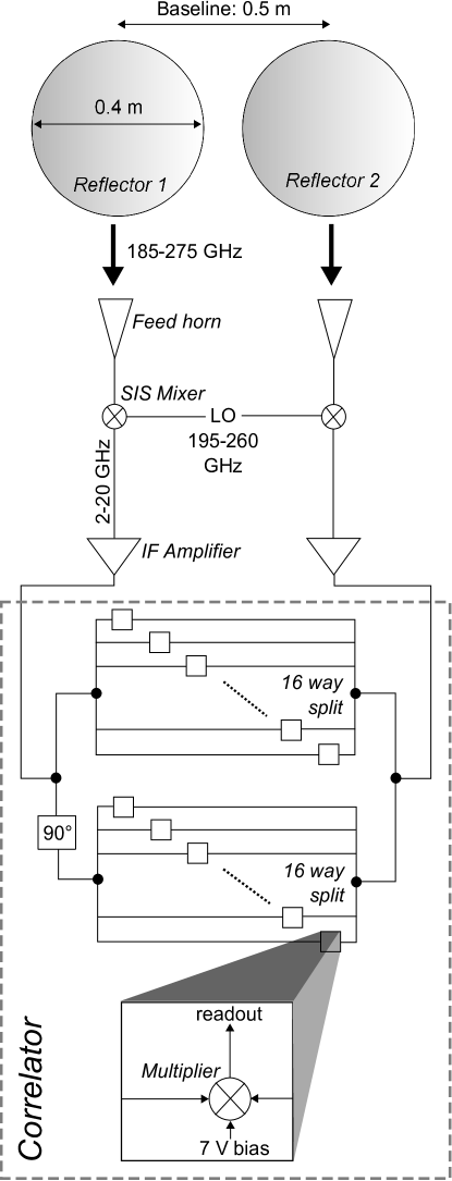
Improvements in front-end receiving systems and in the back-end signal processing systems are needed to help progress the study of the CMB. Increasing the system bandwidth allows more precise radiometry and hence more sensitive measurements. Here we describe a cross-correlator that covers the very wide bandwidths needed to gather signals for measurements of tiny deviations from the CMB’s 2.73 K blackbody radiation temperature. Wide bandwidths are needed to fully exploit the windows in the atmospheric transmission in the millimeter wavebands, which are typically many tens of GHz wide. This correlator operates over the frequency range 2–20 GHz, and is the back-end for a prototype wide-band interferometer, GUBBINS [1], currently under development. This telescope is a millimeter-wave (185–275 GHz) single-baseline interferometer employing SIS mixers and very wide bandwidth low-noise IF amplifiers. A schematic of the instrument is shown in Fig. 1.
Other broadband analog correlators which have been used in experiments devoted to the CMB have bandwidths up to 16 GHz (e.g. [2], [3]). The correlator we discuss here has a combination of broader bandwidth, lower complexity and lower power dissipation than previous correlators used in CMB interferometry, properties that enable the construction of larger interferometric arrays.
II Digital vs. Analog Correlators
Correlators can be implemented using either analog or digital technology. Analog correlators use voltage multiplier circuits and integrators to correlate the two signals, while in digital correlators the signals are digitized, and multiplied and integrated using digital circuits. If the correlated signal must be split into many frequency channels for high resolution spectroscopy, or the path lengths from antennas to the correlator need to be equalized by relatively large time delays, digital correlators are the common choice because of the straightforward hardware requirements. However, analog correlators can offer a more economic solution if there is no requirement for fine frequency resolution or large delays, but very large continuum bandwidth, low power consumption and reduced complexity are required.
For example, we can compare our analog implementation of the single-baseline GUBBINS correlator with an equivalent implmentation using CASPER[4], a hardware/firmware system of digital processing equipment optimized for radio astronomy, which is currently being used for several large correlator projects[5]. A typical CASPER-based implementation would employ samples/sec, 8-bit analog-to-digital converters, each of which can sample a 500-MHz baseband signal. To cover our 2–20 GHz band for two antennas would require 72 such converters, plus a large amount of RF electronics (mixers, LO combs, filters) to split and down-convert the signal bands in to appropriate baseband channels. The signal correlation would be carried out using field-programmable gate arrays (FPGAs), for example the Xilinx Virtex 5 on the ROACH processing board. Each ROACH can host two dual-channel A/D converter cards, so 18 ROACHes would be required. Each ROACH board can provide up to op/sec of processing (with full utilization of the FPGA multipliers). The processing rate required for our correlator is given by the product of the Nyquist data rate ( samples/sec), the number of lag channels (16) and the number of real multiplies per complex multiply (4), giving op/sec. With realistic utilization levels this could be comfortably handled by the 18 ROACHes, provided they were interconnected with an 18-port 10-gigabit ethernet switch. The total cost of this hardware would exceed $100,000.
It can be seen however, that the bottleneck is more in the signal acquisition rather than processing; development of low bitcount digitizers with sampling rates of many tens of gigasamples per second, along with increases in the rate of digital operations on a single device, may eventually swing the economics in favour of a digital solution.
III Correlator Architecture
The key design decisions in the implementation of a very broadband correlator relate to the choice of frequency band, whether the signal band is divided into narrower channels before or after correlation, the type of non-linear element used to perform the multiplication, and the method of physical distribution of the signals to form the required cross-correlations.
Some previous correlators have achieved high bandwidth by splitting the IF band in to multiple sub-bands which are downconverted to a common baseband. For example, the CBI/DASI correlator [2] splits a 2–12 GHz IF band into ten 1–2 GHz bands using filter-mixers. The signals are then correlated using ten identical units in which Gilbert cell multipliers are placed at the intersections of crossing striplines. This method has the advantage of keeping the bandwidth of the individual correlation units small, but the filter-mixer bank is a significant additional complication. Given the recent availability of off-the-shelf microwave components up to 20 GHz, one of our goals was to process a large IF bandwidth without further explicit splitting and downconversion.
The non-linear multiplying element is also a key design choice. Active multipliers (Gilbert cells) [2], balanced mixers [3], and diodes [6] are all possible choices. For this project we use a 20-GHz bandwidth custom-made Gilbert cell multiplier developed specifically for use in astronomical correlators. Individual monolithic microwave integrated circuit (MMIC) chips contain a four-quadrant Gilbert cell multiplier [7] fabricated in InGaP/GaAs heterojunction bipolar transistors (HBT) technology. Transistor speed limits the upper end of the multiplier’s usable response to between 20 and 25 GHz. The frequency response of test amplifiers on the same wafers suggested transistor of about 70 GHz, in reasonable agreement with the foundry’s [8] nominal values for their process at the time of the fabrication in 2002. Integrated bias blocking capacitors at the inputs set the low-frequency response end to about 1 GHz. Resistive matching at the chip edges provides an excellent match across the input band. An integrated differential postamplifier buffers the multiplier output and provides further gain. More detailed information is available in references [9],[10] and [11].
Having chosen to use a single wide IF band we need to provide frequency resolution by means of a lag correlator, in which the outputs of multiple correlations with different lag spacings are Fourier transformed to give the cross-frequency spectrum. In general a lag correlator samples a correlated signal from two antennas at fixed time delays. These are normally set to the Nyquist rate in order to recover the spectrum of a signal with bandwidth . However, depending on the type of interferometer and other hardware restrictions, different delay structures are possible [12]. In general, the relationship between the interferometer antenna diameter , its longest baseline , and the RF and IF frequencies dictates the need for negative and positive, or only positive delay lines. If
| (1) |
then the additional time delay for a signal originating from the edge of the beam instead of the center is much smaller than a single lag delay in the correlator. In this case it is sufficient to sample positive delays only at Nyquist rate, since the centre of the cross correlation function (CCF), the so-called zero lag, is fixed in lag space. All the complex spectral information is contained in the positive half of the CCF. If the inequality (1) does not hold, negative and positive delays have to be used in order not to lose signal at the beam edges, since sources originating at different places in the beam can introduce positive or negative lags that are significant compared to the coherence time. In this case the lags have to be sampled with twice the Nyquist lag spacing.
Both architectures depend on the availability of a broadband 90∘ phase shifter: the complex correlator produces 0∘ and 90∘ correlations (Fig. 1), which correspond to real and imaginary values, respectively. However, a real correlator can be built without the need of a broadband phase shift, using twice the number of 0∘ correlations with half the lag spacing and no 90∘ correlations [6]. Fourier transformation of the measured values results in the same complex power spectrum.
Experience shows that the use of a complex correlator has practical advantages, especially in the commissioning stages of a telescope, since the complex visibility is available before the signal has been Fourier transformed, and a true phase can thus be measured in each lag channel separately. For this reason we decided to build a complex lag correlator, using commercially available 90∘ hybrids, which although relatively expensive are only required one per antenna. Since equation (1) is valid for the GUBBINS telescope, i.e. the baselines are short, we only measure positive lags, using the Nyquist sampling rate.
In the correlator described below, each frequency band is split into 16 complex channels, and so 32 correlations are necessary for a single baseline. All the correlations for each complex component are combined on a single circuit board and two such modules per baseline are required.
The correct time delay of each lag is essential for the frequency bandwidth of the correlator. The number of lags defines the resolution of a frequency channel. The sampling rate of our correlator is set to 20 GHz, therefore the channels covering a total frequency range 0–20 GHz have a width of 1.25 GHz each. In order to suppress aliasing at the upper frequency limit a steep cut-off at 20 GHz is necessary. Alternatively the highest one or two channels can be discarded. For GUBBINS we implemented a filter for signals above 18 GHz. For further details on analog lag correlators see for example [13] or [6].
Since the response of the multiplier chips only drops off slowly below 2 GHz and above 20 GHz, a somewhat higher bandwidth of approximately 1–23 GHz with the appropriate lag spacing and calibration should in principle be possible, but has not been investigated yet.
IV Correlator Design
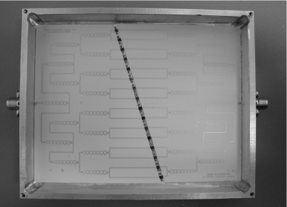
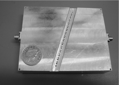
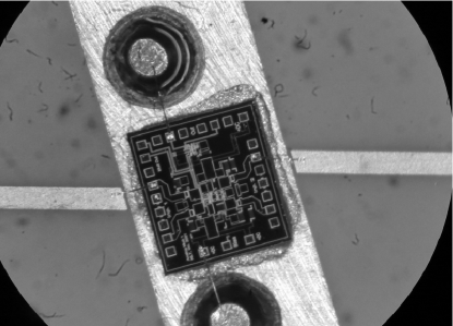
Photos of a single correlator module (half of a complex correlator) can be seen in Fig. 2. On each board two splitter trees of broadband Wilkinson dividers split the incoming signals from the two antennas of a baseline into 16 identical signals. All signals are then correlated after appropriate time delays using the custom-made Gilbert cell multipliers.
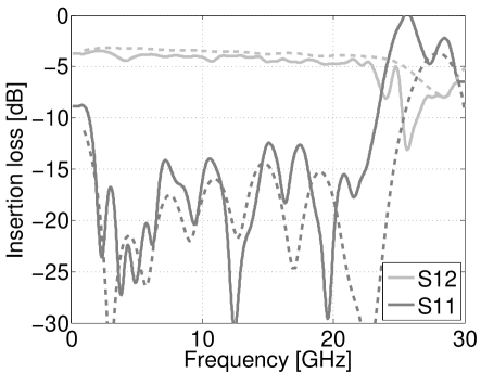
The correlator module shown consists of a single-layer microstrip board on a 10-mil alumina substrate with a dielectric constant of . The two splitter trees contain fifteen Wilkinson power dividers, arranged in a binary tree. The power dividers use seven elements in order to give sufficient bandwidth with adequate insertion loss and matching, and work up to approximately 23 GHz. Lumped element resistors have too large parasitic reactances to work well over this bandwidth so we use thin film resistive sheet to form the resistive elements between the rings which provide for high output isolation. We experimented with Duroid substrates, using OhmegaPly nickel-phosphorus film underneath the copper traces to form the resistive elements by a pure etching process, but we found that the resulting slope of insertion loss with frequency was excessive. Instead we have adopted alumina substrate with deposited tantalum nitride thin-film resistive elements, which gives much better frequency response. Measured results compared to simulations of a single splitter can be seen in Fig. 3.
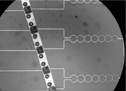
Placed between the two splitter trees are 16 multiplier chips (Fig. 1 and 2). Due to the delay steps they are oriented diagonally to the delay lines. The Nyquist rate here is and corresponds to 7.5 mm delay difference from one multiplier to the next (the lag spacing) in vacuum. Due to the high dielectric constant this is reduced to 2.92 mm on the alumina board. Since the signals are counter-propagating, the horizontal distance between two adjacent multiplier chips is only half that distance i.e. 1.46 mm. The signals from the microstrip lines are directly wire bonded to the input pads of the multiplier chips which have input impedance. There are two metal feed-through pins on either side of each chip. One is used for the bias supply to the multiplier and the other for the low frequency output signal from the multiplier. These connect to a FR4 circuit board, which is mounted on the back of the correlator box, containing further analog gain, buffering and filtering. The signals are then passed via a backplane to a 16-channel digitizer board where the signals are sampled at 14-bits resolution and 2.8 Msamples/sec, and integrated in an FPGA.
V Signals and Phase Switching
The desired correlated signal of the observed astronomical object is in general deeply buried inside uncorrelated noise. The undisturbed extraction of this average correlated signal voltage is the goal of a cross-correlator. Uncorrelated noise in the system has different sources. The main contributions are receiver noise, atmospheric temperature, antenna spillover and ohmic losses in the system.
However, there are many additional sources of signal contamination in the signal path after the antenna, which can be strongly correlated, e.g. pick-up of terrestrial signals, temperature fluctuations, mains pick-up and cross talk between antennas. Therefore a phase-switching system is normally introduced at the earliest possible point in the receiver chain in order for these signals to be eliminated. For this the signals from the different antennas are modulated by orthogonal periodic functions, e.g. Walsh functions.
Phase-switching only suppresses signals with longer coherence time then the repeat period of the switching functions. Therefore, a high phase-switching frequency is preferred. However, for accurate demodulation of the switched signal, the power in the modulated signal must be contained within the video bandwidth of the detectors. If the loss of signal due to filtering is to be less than 0.1%, a basic frequency of about a thousand times lower than the video bandwidth is required.
The multiplier’s video bandwidth is approximately 10 MHz, but in order to reduce the required sampling frequency of the digitizers (which is fixed at 2.8 Msamples/sec for the sampler board available to us) this is filtered down to 800 kHz and therefore a phase switching frequency of less than 1 kHz is required. Further details in the next section about low frequency noise show that this is very well possible. A more detailed discussion of suppression levels that can be obtained by phase switching can be found in [2].
VI RF Measurements
Here we present the results of testing four prototype correlator modules, of which one is shown in Fig. 2.
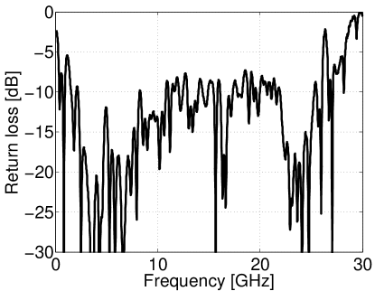
VI-A Return Loss
The return loss at the inputs to the correlator board is shown in Fig. 4. It is well matched across the band of 2–20 GHz.
VI-B Lag Spacing
Regular lag spacing (the electrical path distance between to adjacent multipliers) is important for the performance of the correlator. Variations in the lag spacing result in an irregular Fourier transform, which is not in general inferior to a regular one. However, in the presence of noise, this leads to a reduction in signal-to-noise; some power will be scattered from one frequency channel to another [13]. Calibration schemes can minimize this effect of irregular lag spacing.
As mentioned above, delays between the multipliers should ideally be 7.5 mm in free space, or , which corresponds to about 2.92 mm in alumina. Some degree of distance variation is expected due to, for example, small irregularities in the printing process of the microstrip lines, placing of the multiplier chips and variations in both the dielectric constant of the substrate and the bond length to the multiplier chips. Dispersion in the microstripline transmission lines causes the distance also to vary across the band.
We measure the lags directly by feeding a CW signal into both inputs to the cross-correlator, with an additional delay at one input. When the signal is stepped in frequency the response of a single lag is a sine wave as a function of frequency and the wavelength of this sine wave depends on the lag’s absolute distance from the zero lag. The difference in wavelength for different lags makes it possible to calculate the relative distances very accurately. For more details see [14].
Fig. 5 shows the measured delays between adjacent points of correlation. The average delay step is 7.40 mm which means that the cut-off frequency of the Fourier transform is 20.3 GHz. The biggest relative lag error is 9% and the standard deviation is 3.8%. The lag errors are small and stable with time, which means their effect on the final transformed spectrum can be removed with suitable calibration. Path and phase errors due to the external hybrid and fixed cables are also stable and are removed by the same calibration procedure.
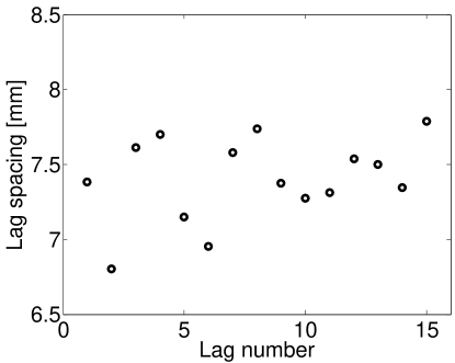
The lag errors are within the expected range and the effect on the recovered signal, namely signal scattering between frequency channels, can be minimized using the correct calibration. Calibration can either employ a set of known frequencies which are used to measure the position (phase) and frequency response (amplitude) of each multiplier, as in these tests, or alternatively a known broadband signal (e.g. an astronomical source) that is swept in delay can be used to measure the same properties. Provided that the lag errors are small compared to the lag spacing, the loss in signal-to-noise in this calibration procedure is small. If the error approaches a whole lag spacing then the information sampled by each lag becomes degenerate and signal-to-noise is permanently lost.
VI-C Frequency Response
The frequency response of the correlator can be seen in Fig. 6. The variation in response between the channels is less than 2 dB. Comparing the correlator passband to the response of an individual multiplier shows that the splitter tree contributes approximately dB to the slope across the frequency band, the multiplier itself about to dB.
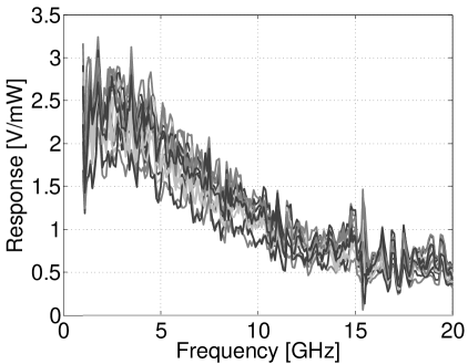
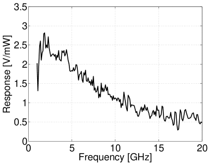
There is a narrow resonance at about 15.5 GHz in several of the channels, whose origin is unclear. This resonance could also be seen in the response of a separate single multiplier chip and therefore is not connected to the splitter tree. The resonance is stronger for lower input power. The common structure between 16 and 18 GHz is also present in the separate individual multiplier chips.
The other small scale variations in the passband are caused in part by measurement noise and amplitude and phase errors in the 90∘ hybrid, which has been used to measure real and imaginary values. Also, some of these variations can be attributed to passband variations of the microstrip circuit, but in general the response is well behaved.
VI-D Power Response
The multiplier detects the correlated noise power, ideally producing the true linear product of the input voltages. If the multiplier is operating close to compression, then even small changes in the power level will result in a change in small-signal responsivity, and hence a change in the effective gain of the system. The power response of the correlator is shown in Fig. 7. The responsivity is constant across the full bandwidth up to well-defined power levels. From these data the maximum input power as a function of frequency can be calculated. The maximum input level for 10% ( dB) deviation from the linear response is shown in the lower plot of Fig. 7. In astronomical observations, where calibration can be used to frequently re-measure the system responsivity, a dB compression can be used as a limit, increasing the maximum input power level by about 2 dB. This changes the noise statistics by an acceptable small amount and a negligible amount of power is converted to harmonics of the orignial signal [15].
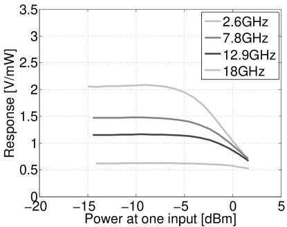
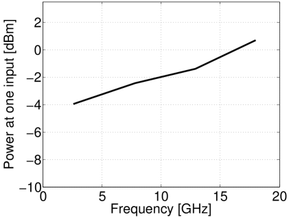
This defines the level and shape of a broadband input signal. For a cross-correlator, where the correlated part of the signal is deeply buried inside the uncorrelated noise from the front end, a broadband signal in the range 2–20 GHz should have a positive slope of 6 dB across the band and a signal level of approximately dBm for dB noise compression and 0.5 dBm for dB noise compression. For signal to noise reasons, as explained in Section VII, the signal should not drop much below dBm.
VI-E Video Bandwidth
The video bandwidth of the correlator is constant across the band but varies slightly between channels. A value of 10 MHz ( dB in output voltage) or 5 MHz ( dB in output power) has been measured.
VII Noise Behaviour
The response of the correlator to an input signal has two components. A correlated noise-like signal of power and spectral density will produce an average (DC) output voltage:
| (2) |
where is the spectral responsivity of the correlator channel. The second component, the noise of the output signal, is:
| (3) |
where and are the video and IF bandwidths, or the output and input bandwidths of the correlator; here 10 MHz and 18 GHz, respectively. The last equation is valid for correlated or uncorrelated noise and therefore in (3) is the spectral power density of the correlated and uncorrelated signals added together.
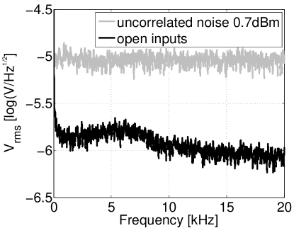
The multipliers also produce intrinsic output noise without input. They are high-noise devices and some care has to be taken to find the correct signal levels and phase switching frequency in order for the overall signal-to-noise not to be dominated by noise contributions from the multipliers. Fig. 8 shows the noise voltage spectrum of one channel with open inputs, along with the equivalent power spectrum when the correlator is fed with uncorrelated broadband noise at the level 0.7 dBm, simulating the (noise-dominated) signal expected from the antennas of an interferometer. All channels have very similar noise levels with a typical voltage spectral density of less than at frequencies above 1–2 kHz, which is a factor of 8–10 lower in voltage (18–20 dB in power) than the thermal noise spectrum due to the signal. The knee frequency for the correlator noise is about 500 Hz, and the correlator noise signal does not exceed the input noise signal above 100 Hz. Therefore provided the signal is modulated by phase switching at a higher frequency than 100 Hz, the correlator will not introduce excess noise to the measurement.
VIII Readout Electronics
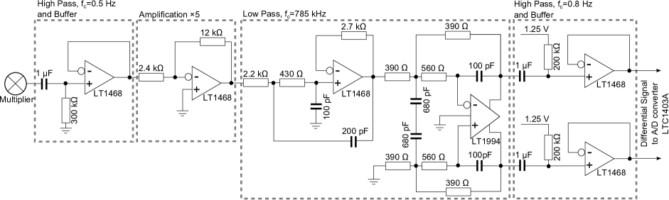
The purpose of the readout electronics is to buffer the output signals from the multipliers, amplify and filter them before they can be digitised by a set of A/D converters. The principal signal chain after the multiplier is shown in Fig. 9.
As described above, the multiplier output contains the phase switched correlated signal buried in uncorrelated noise. In order to have a good rejection of any unwanted correlated signals picked up after the receiver, low leakage between different orthogonal switching functions is necessary. For this the shape of the switching function has to be sampled very accurately. This requires high sampling rates in the A/D converter (here 2.8 Msamples/sec) and careful design of the signal filters.
To avoid aliasing, the analog electronics should filter out signals above 1.4 MHz. However, an undisturbed square wave requires high signal bandwidth and small phase distortions. Therefore a compromise between steep frequency cut-off, low phase distortions and limited circuit complexity had to be found. An active four-pole Bessel filter using a relatively small number of components was implemented.
At the lower end of the frequency band similar restrictions apply. The multiplier signal contains an offset DC voltage, which depends on the bias supply voltage and has to be filtered out. However, a high cut-off frequency produces a droop which distorts the square wave. Therefore the corner frequency of the high pass filter has to be set as low as possible, in our case below 1 Hz.
The detailed circuit layout of the readout electronics is also shown in Fig. 9. The multiplier bias voltage is 7 V and the output DC offset 6 V. The first low-pass filter which blocks this DC level consists of a capacitor of and a resistor of . This is small compared with the input impedance of the first buffer stage and therefore the high-pass 3 dB frequency is 0.5 Hz. However, the relatively high resistor value produces a small DC offset due to the input bias current of the LT1468. This is a maximum of 40 nA and therefore the offset of the first stage is about 12 mV but will be amplified in the second stage.
In the next stage the signal is amplified slightly. For typical IF signal levels the multiplier produces a noise-like random signal of about , and approximately 120 mV peak-to-peak. Since the input range of the ADC is 0 to 2.5 V and the highest peaks of the noise signal should be within this range, we only amplify by a factor of 5.
The next two stages make up a 4-pole active Bessel filter with a 3 dB frequency of 785 kHz and a rejection at the Nyquist frequency of 1.4 MHz of . The first stage is a Sallen-Key design and the second a multiple-feedback filter. In addition the second stage produces a differential signal, since this is required as input by the A/D converter.
After the filter the signal is elevated to a DC level of 1.25 V since the A/D converter’s input range is 0 to 2.5 V. Simultaneously a second high-pass filter blocks any small DC levels of the previous stages. However, the input bias current of the following LT1468 across these last resistors produces a new offset voltage. Since the signal is now differential the input offset current, the difference between the inverting and non-inverting input bias currents, sets the DC offset level. For the LT1468 this is below 50 nA. In fact the component has mainly been chosen for its small input bias current. In any case, this DC offset will be suppressed by phase-switching as long as the variations, for example due to temperature, are slower than the phase switching frequency.
The last buffer is necessary since the bias input current of the A/D converters is comparatively high and would produce a much larger voltage offset. Finally, the A/D conversion is done on a separate board using LTC1403A with 14 bit resolution. The demodulation and further integration of the signal is then done in software in an FPGA on the same board.
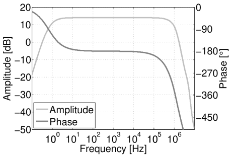
The simulated results of the full readout chain are shown in Fig. 10. The distortion of a square wave through the full readout circuit is very small. The rise time is about , which for a single baseline and 10 kHz phase switching corresponds to a reduction in correlator output of 0.7%. The droop of the signal is only 0.05% of the signal level after .
These values are also important for potential cross talk between different baselines since a distortion of the square wave reduces orthogonality between the phase switch functions. The effect due to rise time can be best reduced by blanking out the response of the correlator for that period. Depending on the number of baselines and therefore the period of the highest order switching function this can reduce the observing time substantially. In the case of a single baseline with 10 kHz phase switching this would reduce observing time by about 1.4%. The droop will invariably increase cross talk between baselines since demodulating a phase switched signal with an orthogonal function does not reject the signal fully. Here it would give a rejection of about .
IX Conclusions
We have presented an ultra-broadband analog Fourier transform correlator. The instrument works well over 2–20 GHz with a possible maximum bandwidth of 1–23 GHz. The frequency band is split into 16 complex channels, each 1.25 GHz wide. The response of the correlator is well behaved over the band and the signal-to-noise of the system is not limited by the cross-correlator. We have also described the low frequency readout electronics necessary to digitise a fully phase-switched astronomical signal.
Acknowledgment
The authors would like to thank J. J. John of the Oxford Physics Central Electronics group for assistance with the readout electronics and Adam Coates for assistance with the noise power spectrum measurements.
References
- [1] P. K. Grimes et al., “A novel heterodyne interferometer for millimeter and submillimeter astronomy,” in 19th International Symposium on Space Teraherz Technology, Groningen, April 2008.
- [2] S. Padin et al., “A wideband analog correlator for microwave background observations,” “ IEEE Trans. Instrum. Meas, vol. 50, pp. 1234–1240, 2001.
- [3] C.-T. Li et al., “AMiBA wide band analog correlator,” “ ApJ, vol. 716, pp. 746–757, 2010.
- [4] D. Werthimer et al., “Open source hardware and gateware for wide-band radio astronomy instrumentation,” in 2009 USNC/URSI Annual Meeting, Jan. 2009.
- [5] A. Parsons et al., “A scalable correlator architecture based on modular fpga hardware, reuseable gateware, and data packetization,” PASP, vol. 120, pp. 1207–1221, Nov. 2008.
- [6] C. M. Holler et al., “A 6-12 GHz analogue lag-correlator for radio interferometry,” Astronomy and Astrophysics, vol. 464, pp. 795–806, 2007.
- [7] B. Gilbert, “A precise four-quadrant multiplier with subnanosecond response,” IEEE J. Solid-State Circuits, vol. 3, pp. 365–373, 1968.
- [8] Global Communication Semiconductors, Inc., Torrance, CA.
- [9] A. I. Harris, “Gilbert cell multiplier measurements from 2-18.5 GHz,” Tech. Rep., January 28 2002. [Online]. Available: http://www.astro.umd.edu/~harris/docs/multmeas1.pdf
- [10] ——, “Gilbert cell multiplier measurements III: Response from 2-30 GHz,” Tech. Rep., June 07 2002. [Online]. Available: http://www.astro.umd.edu/~harris/docs/multmeas3.pdf
- [11] ——, “Maas gilbert cell multiplier measurements V: Chips from the second (production) run,” Tech. Rep., July 02 2003. [Online]. Available: http://www.astro.umd.edu/~harris/docs/mults_5.pdf
- [12] A. R. Thompson, J. M. Moran, and G. W. Swenson, Interferometry and synthesis in radio astronomy. Malabar, FLA: Krieger Pub., 1991.
- [13] A. I. Harris and J. Zmuidzinas, “A wideband lag correlator for heterodyne spectroscopy of broad astronomical and atmospheric spectral lines,” Rev. Sci. Instrum, vol. 72, p. 1531H, 2001.
- [14] C. M. Holler, “Correlator and antenna design for the Arcminute Microkelvin Imager,” Ph.D. dissertation, Cambridge University, Cambridge, United Kingdom, 2003.
- [15] A. I. Harris, “Precision radiometry and the APHID 22 GHz water line monitor,” ALMA Memo #307, May 2000.
| Christian M. Holler was born in southern Germany in 1973. He studied physics at the Ludwig-Maxmilians-Universität in Munich, Germany and earned his Diplom in 1999. In 2003 he received his PhD in the field of astrophysics and instrumentation at the Cavendish Laboratories, Cambridge University, United Kingdom. After returning to Munich, Germany he successfully pursued entrepreneurial work. In early 2007 he joined the experimental cosmology group at the University of Oxford as a postdoctoral research assistant, where he was involved in several instrumentation projects. In September 2009 he was appointed a Professor at the University of Applied Sciences in Esslingen, Germany. |
| Michael E. Jones was born in Wrexham, UK, in 1966 and studied Natural Science and Electrical Science at Cambridge University. He obtained a PhD in Radio Astronomy at the Cavendish Laboratory, Cambridge in 1990 and subsequently worked there as a Research Associate and Senior Research Associate. In 2005 he was appointed first as a Lecturer and then as Professor of Experimental Cosmology at the University of Oxford Department of Physics. |
| Angela C. Taylor was born in Dartford, UK in 1975 and studied Natural Sciences at Cambridge University, earning a PhD in astrophysics at the Cavendish Laboratory Cambridge in 2002. She continued to work in the field of astrophysics and instrumentation as a postdoctoral research assistant at the Cavendish Laboratory until 2005 when she moved to the University of Oxford as a founding member of the experimental cosmology group. Since January 2005 she has been an STFC Postdoctoral Research Fellow and then a Royal Society Dorothy Hodgkin Research Fellow working on a range of experimental cosmology projects at the University of Oxford. |
| Andrew I. Harris received his Ph.D. in Physics from the University of California at Berkeley in 1986. He is a Professor in the Department of Astronomy and an Affiliate Professor in the Department of Electrical and Computer Engineering at the University of Maryland, where he specializes in experimental astrophysics and astronomical instrumentation. |
| Stephen A. Maas earned his Ph.D. in Electrical Engineering from the University of California at Los Angeles in 1984. Since then, he has been involved in research, design, and development of low-noise and nonlinear microwave circuits and systems at the National Radio Astronomy Observatory (where he designed the receivers for the Very Large Array), Hughes Aircraft Co., TRW, and the Aerospace Corp. For several years he was a member of the Electrical Engineering Faculty at UCLA. He is now Director of Technology at AWR, specializing in nonlinear circuit simulation technology. He teaches periodically at UCLA, both regular and extension courses. He is the author of several books on mixers and other nonlinear devices. |