On the Optical Properties of Ag+15 Ion-beam-irradiated TiO2 and SnO2 Thin Films
Abstract
The effects of 200-MeV Ag+15 ion irradiation on the optical properties of TiO2 and SnO2 thin films prepared by using the RF magnetron sputtering technique were investigated. These films were characterized by using UV-vis spectroscopy, and with increasing irradiation fluence, the transmittance for the TiO2 films was observed to increase systematically while that for SnO2 was observed to decrease. Absorption spectra of the irradiated samples showed minor changes in the indirect bandgap from to eV with increasing irradiation fluence for TiO2 while significant changes in the direct bandgap from to eV were observed for SnO2. The observed modifications in the optical properties of both the TiO2 and the SnO2 systems with irradiation can be attributed to controlled structural disorder/defects in the system.
DOI:10.3938/jkps.61.1609
pacs:
78.66.Li, 68.55.-a, 78.20.Ci, 71.20.NrI Introduction
Due to increasing interest in electronics and optoelectronics, among the wide-band-gap semiconductors, TiO2 and SnO2 are being considered as the most promising materials in view of their unique properties and various future technological applications. These applications boast their moderate price, high-volume, nontoxicity and chemical stability. In addition, these materials offer the possibility of integrating their magnetic and electronic properties in spintronic devices by using both the spin and the charge of electrons r1 ; r2 .
TiO2 is a very interesting and versatile material with a wide range of applications, including use in microelectronics due to its high dielectric constant and in optical coatings due to its high refractive index r3 ; r4 ; r5 ; r6 ; r7 ; r8 . It also has excellent optical transmittance in the visible and the near-infrared regions. TiO2 exists in three crystalline polymorphs: rutile, anatase, and brookite with band gap values of , , and eV, respectively r9 . Among the different TiO2 polymorphs, anatase (tetragonal, ) is a metastable phase that contains four shared edges per octahedron (the highest condensation of TiO6 octahedra) and is known to be useful for photocatalysis with response to ultraviolet photons. The rutile (tetragonal, ) is the thermodynamically most stable phase at all temperatures and is formed by sharing two edges per octahedron (the lowest condensation of TiO6 octahedra) with the largest index of refraction. The brookite (orthorhombic, ) is the most distorted phase and shares three edges per octahedron. The properties of TiO2 significantly depend on the crystalline phases, i.e., anatase, rutile, or brookite, and on the morphology of the material r10 .
On the other hand, tin dioxide (SnO2) has been investigated in the view of potential technological applications in catalysis, gas sensor technology, etc. r11 ; r12 ; r13 because of the high carrier density, optical transparency, wideband gap ( eV), and remarkable chemical and thermal stabilities. SnO2 exists in the most important form of the crystalline phase, known as cassiterite, with a rutile (tetragonal, ) structure. Another form of SnO2 with an orthorhombic structure is known to be stable only at high pressures and temperatures.
Many deposition techniques (pulsed laser deposition, sol-gel deposition, etc.) have been employed to synthesize TiO2 and SnO2 thin films, although magnetron sputtering remains the preferred method due to its better coating uniformity, process versatility, large-area coating capability and more freedom in selecting the deposition conditions r14 . Any mechanism that affects the lattice structure of the TiO2 and the SnO2 systems also influences their electronic structures and optical properties. Swift heavy ion (SHI) irradiation is one of the mechanisms that have been used to tailor the material properties by modifying its electronic structure r14 ; r15 ; r16 . Radiation-induced defects produced in the material are well documented to depend entirely upon the energy loss processes, namely, nuclear energy loss (elastic process), and electronic energy loss (inelastic process), involved during the passage of ions through the target material. In the high-energy region, due to dense electronic excitations, SHIs induce point/cluster/columnar defects and structural disorder, depending upon the extent of the electronic energy loss mechanism in the system. Previous studies on the TiO2 and the SnO2 systems only focused on the SHI-induced modifications in the electronic structure, orbital anisotropy and magnetic properties r15 ; r16 . Thus, other properties, such as the optical properties, need further study. This experimental study was conducted to observe the changes in the optical transmittance, absorption and band gaps of TiO2 and SnO2 thin films irradiated with a 200-MeV Ag+15 ion beam at various irradiation fluences ranging from to ions/cm2 which is different from what is largely reported.
II Experiment and Discussion
Pure titanium (II) oxide (TiO) and SnO2 compounds (purity 99.9%) were used as the starting materials for the depositions of the thin films. TiO2 and SnO2 films, approximately -nm thick, were deposited on cleaned sapphire single-crystal substrates by using a RF magnetron sputtering technique. The pure oxide materials were ground into a fine powder in an agate mortar; then, mixtures were pressed in the form of circular targets of mm in diameter by applying a pressure of tons in a hydraulic press. The targets were sintered at C for h. Prior to filling the chamber with sputtering gas, it was evacuated to a base pressure of Torr by using a turbo-molecular pump. The deposition was carried out in a partial pressure of mTorr of an oxygen and Ar gas mixture (1:1), keeping the substrate temperature at C and RF power at W. After deposition, the films were annealed in-situ at C in oxygen for h. The deposited thin films were irradiated with 200-MeV Ag+15 ions at fluences of , , and ions/cm2 at room temperature (RT) by using the 15UD tandem accelerator at the Inter-University Accelerator Center, New Delhi, India.
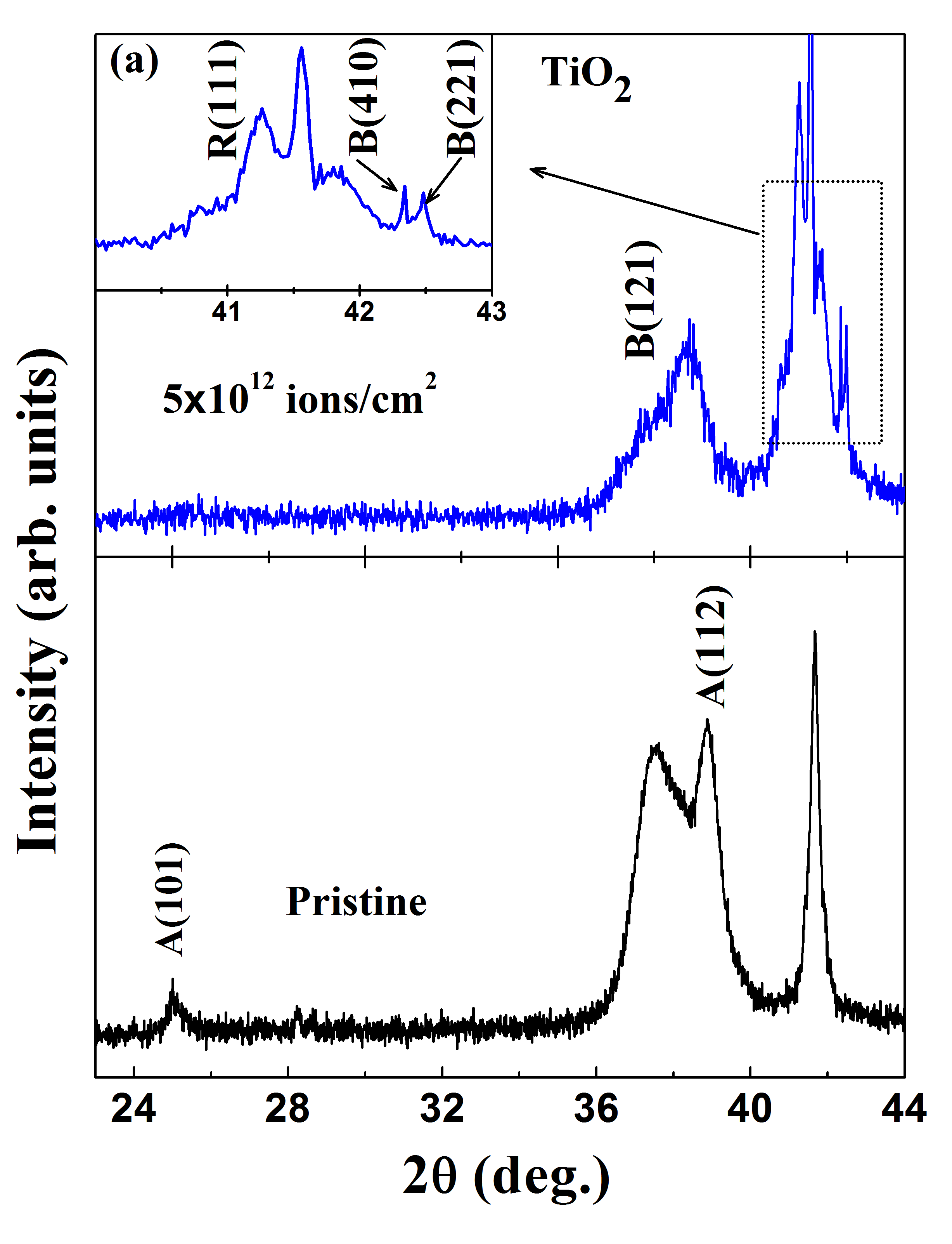
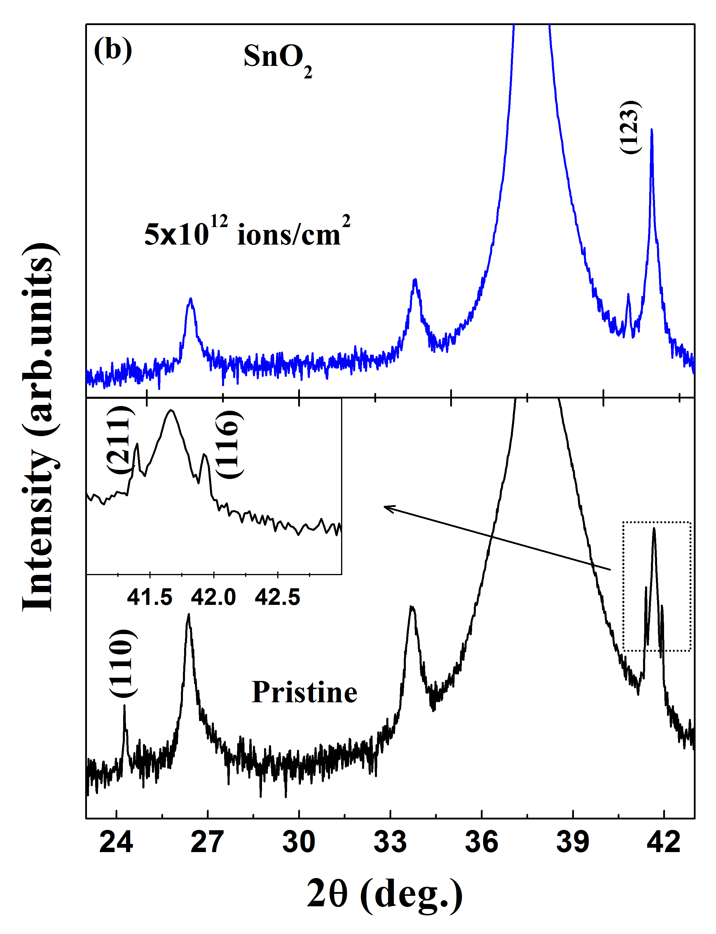
The structural analysis of the pristine and the irradiated TiO2 and SnO2 films was carried out using high-resolution X-ray diffraction (HRXRD) with at the bending magnet 1D XRS KIST-PAL beamline of the Pohang Accelerator Laboratory (PAL), Korea. The HRXRD profiles are shown in Fig. 1(a) for the pristine and the SHI irradiation TiO2 thin films. As shown in Fig. 1(a), the pristine sample has a tetragonal anatase structure (JCPDS, Card No.84-1286) while on irradiation at the highest SHI fluence of ions/cm2, the inset in Fig. 1(a) clearly shows mixed peaks of the brookite (JCPDS, Card No.76-1937) and the rutile phases of TiO2. The appearance of broader brookite peaks clearly indicates that SHI irradiation has induced structural disorder and/or strain in the films r16 . Figure 1(b) shows HRXRD pattern of the pristine and the SHI-irradiated SnO2 thin films collected at RT. For the pristine sample depicted in Fig. 1(b), it is evident that the characteristic peaks at , and correspond to reflections from the (110), (211), and (116) planes of the orthorhombic phase (JCPDS, Card No.78-1063) of SnO2, respectively. The inset in Fig. 1(b) shows the extended view of the diffraction peaks of the pristine sample. At the highest SHI fluence of ions/cm2, the irradiation causes partial amorphization and/or strain in the SnO2 system. The detailed structural verification of the SnO2 orthorhombic structure and the effect of SHI irradiation on its structure is discussed elsewhere r18 .
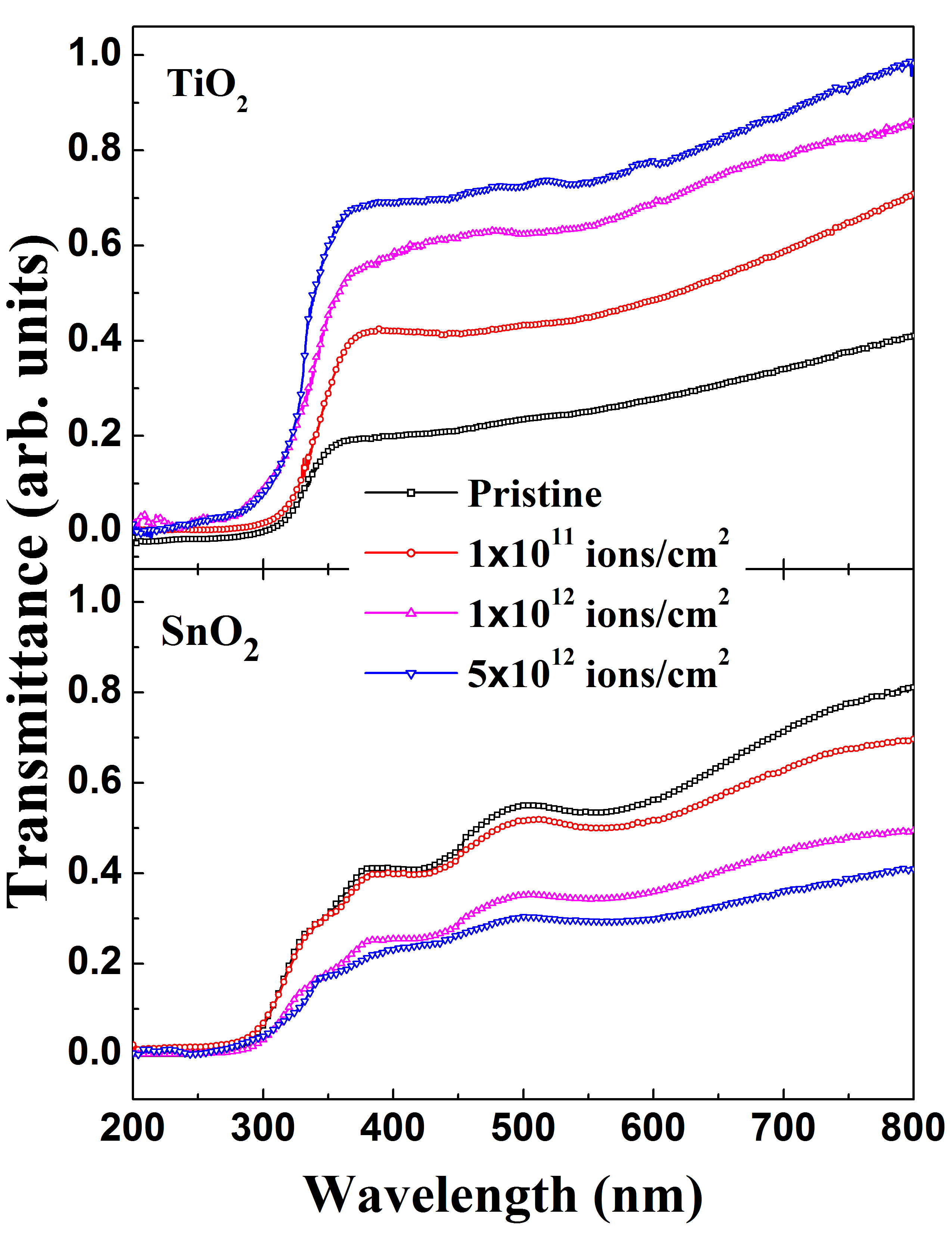
The optical transmittances of the pristine and the irradiated thin films of both oxides were measured by using a Hitachi-U3300 spectrophotometer to collect the transmittance spectra as a function of wavelength in the range of nm at RT with a resolution of nm. Figure 2 presents optical transmittance spectra for the pristine and the SHI-irradiated TiO2 (upper panel) and SnO2 (bottom panel) thin films collected at RT. It is clear from Fig. 2 that the pristine TiO2 film exhibits a transmittance value of about 25% in the visible region at nm. With increasing irradiation (SHI: ions/cm2) fluence, the transmittance increases considerably, which at highest fluence (SHI: ions/cm2) acquires a value of 70%. The increase in the transmittance with increasing SHI fluence signifies that the transparency of the SHI-irradiated TiO2 films is superior to that of the pristine film. On the other hand, the pristine SnO2 film exhibits a systematic decrease in the transmittance with increasing irradiation (SHI: ions/cm2) fluence. In the visible region, the transmittance for the pristine SnO2 film was 50% and decreased to 35% for the highest SHI fluence. Moreover, at nm, the transmittance decreases quickly for all samples for both the oxides materials and approaches zero at nm. This fast decrease in the transmittance is due to strong absorption of light in this region caused by the excitation and the migration of electrons from the valence band to the conduction band. Typical oscillations in the transmittance spectra, particularly for SnO2, may be due to interference of light transmitted through the thin film and the substrate r19 .
Previous studies r16 ; r17 ; r18 revealed that the irradiated TiO2 thin films for the highest SHI fluence exhibited a mixed (dominating brookite + rutile) phase of TiO2 while the SnO2 pristine film was composed of a pure orthorhombic phase of SnO2, and SHI-induced controlled structural disorder (distortion in the SnO6 octahedra) and/or strain in the films. The dominating structure of the brookite phase in the SHI-irradiated TiO2 films and the orthorhombic distortions of the SnO2 lattice could have important implications for the electronic structure and possible optical properties. Therefore, the observed changes in the transmittance of the pristine TiO2 and SnO2 films with SHI fluence can be attributed to TiO6 and SnO6 octahedral distortions, respectively.
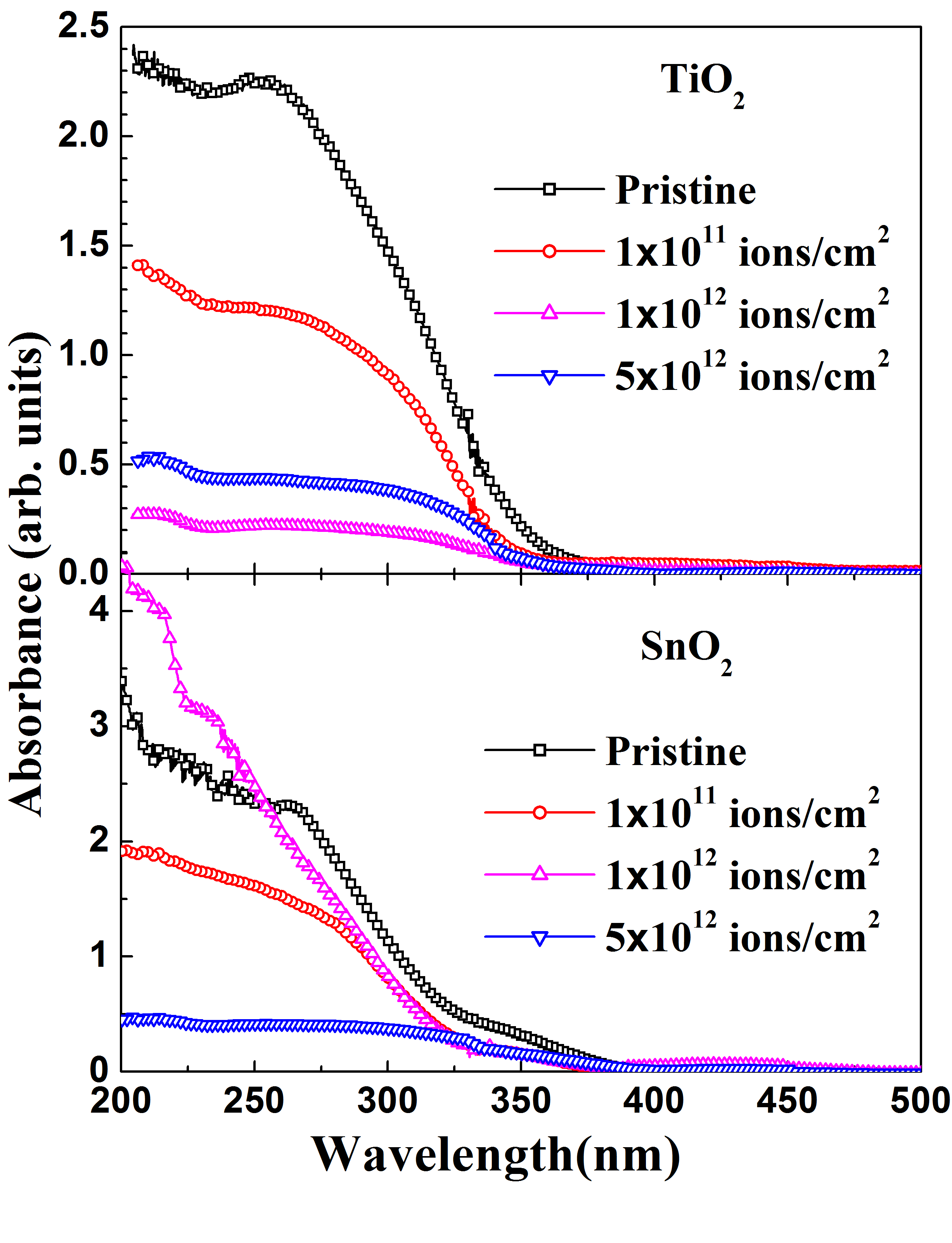
The absorption spectra for the pristine and the irradiated TiO2 and SnO2 films were measured by measuring the absorbance as a function of wavelength at RT. The absorbance is given by
| (1) |
where is the intensity of the incident radiation and is the transmitted intensity. Figure 3 depicts the absorption spectra for the pristine and the SHI-irradiated TiO2 (upper panel) and SnO2 (bottom panel) thin films. The optical absorption spectra of TiO2 showed a clear absorption edge at nm for the pristine TiO2 sample. With increasing irradiation (SHI: ions/cm2) fluence, the absorption edge is slightly shifted to the smaller wavelength side, and at the highest irradiation (SHI: ions/cm2) fluence, it acquires a value of nm. The observed values of the absorption edge deviate from the values reported in the literature r9 . For the SnO2 system, the optical absorption edge of the pristine film was found to be at nm, which is shifted to nm at the highest SHI fluence. In this study, an anomalous trend was observed for the optical absorption edges and the suppression in the maximum absorption with increasing SHI fluence for both the oxide materials. The absorption spectra of both systems reveal that the films grown under the same parametric conditions have low absorbance in the visible/near-infrared region while the absorbance is high in the ultraviolet region. Since SHI induces a controlled structural disorder (TiO6 and SnO6 octahedral distortions) in both the systems, modifications in the absorption spectra can be correlated to changes in the electronic structure as a result of a lowering in the orbital symmetry (i.e., its -, -, and -like character) via strong hybridization effects after irradiation.
The absorption coefficient as a function of photon energy for allowed indirect transitions r17 is given by
| (2) |
and for allowed direct transitions by
| (3) |
where is the absorption coefficient, and are constants for indirect and direct transitions, is Planck’s constant, is the frequency, is the photon energy involved in the indirect transition, and is the band gap energy. The absorption coefficient is obtained from Beer’s law:
| (4) |
In Eq. 4, is the thickness of the measured sample.
The relationship between the absorbance , the absorption coefficient , and the thickness of the film is given by
| (5) |
A plot of versus energy was used to obtain the value of the indirect band gap, and a plot of versus energy was used for the direct band gap by extrapolating the linear portions of the curves to zero absorption.
| Irradiation fluence | Band gap values | |
|---|---|---|
| (ions/cm2) | TiO2 | SnO2 |
| Pristine | 3.44 | 3.92 |
| 3.57 | 3.78 | |
| 3.50 | 3.86 | |
| 3.59 | 3.60 | |
The variations in the band gaps for the pristine and the SHI-irradiated TiO2 thin films are depicted in the Fig. 4(a). The optical transitions for TiO2 have been shown to be predominantly indirect r20 ; r21 while that for SnO2 is direct r22 . The overall values obtained for all the irradiation fluences are higher than the reported values for TiO2, which are usually reported to be around eV. The highest band gap value ( eV) was obtained for the sample irradiated at a fluence of ions/cm2. The band gap values increased until a SHI fluence of ions/cm2, after which they decreased slightly from the value for the sample irradiated at a SHI fluence of ions/cm2, eV. For the irradiated SnO2 samples (see Fig. 4(b)), a trend similar to that of the irradiated TiO2 samples is followed. The highest value for the band gap of the SnO2 sample is for the pristine sample with a value of eV.
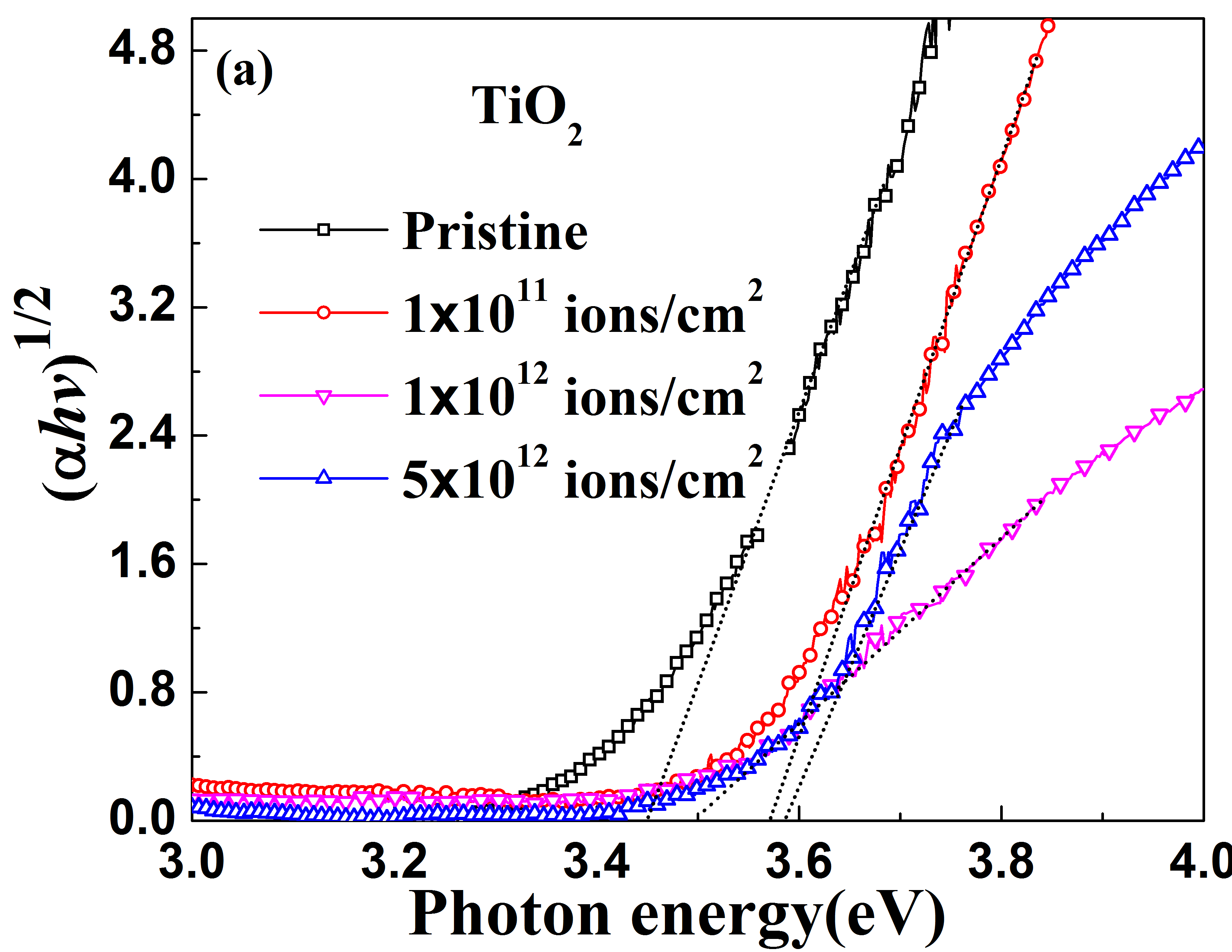
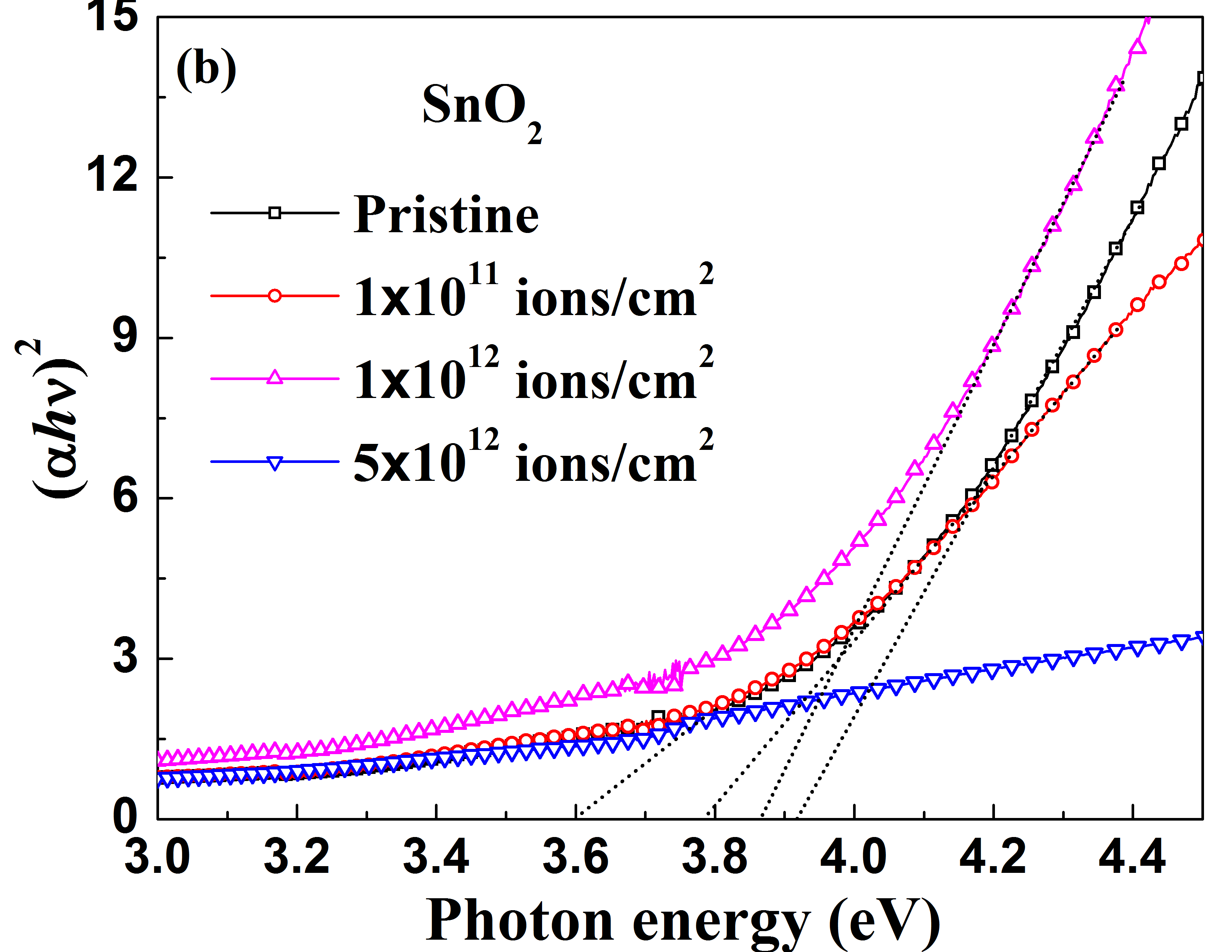
The values decreased until a SHI fluence of ions/cm2, after which the value increased slightly to eV. For the sample irradiated at a fluence of ions/cm2, the value again decreases to eV. Table 1 shows the variations in the band gap energy with irradiation fluence for both the TiO2 and the SnO2 systems. HRXRD data indicate that SHIs create controlled structural disorder in the lattices of oxide materials. This can be responsible for the generation of defect levels near the conduction band, i.e., shallow energy levels, which can give rise to a transition from the valence band to those levels instead of band-to-band transitions. Due to the shallow levels, the band gap is effectively changed. This decrease in the band gap gives an indication of the stoichometric deviation of the irradiated SnO2 and the increase in the oxygen vacancies in the SnO2 lattice. A similar behavior was also reported in a previous work r23 , where the effect of In-doping concentration on the optical band gap of nano-SnO2 was investigated as a function of the calcination temperature. Another possible explanation for the changes in the band gap value may be due to the fact that the density of surface states induced in the SnO2 lattice is modified on irradiation.
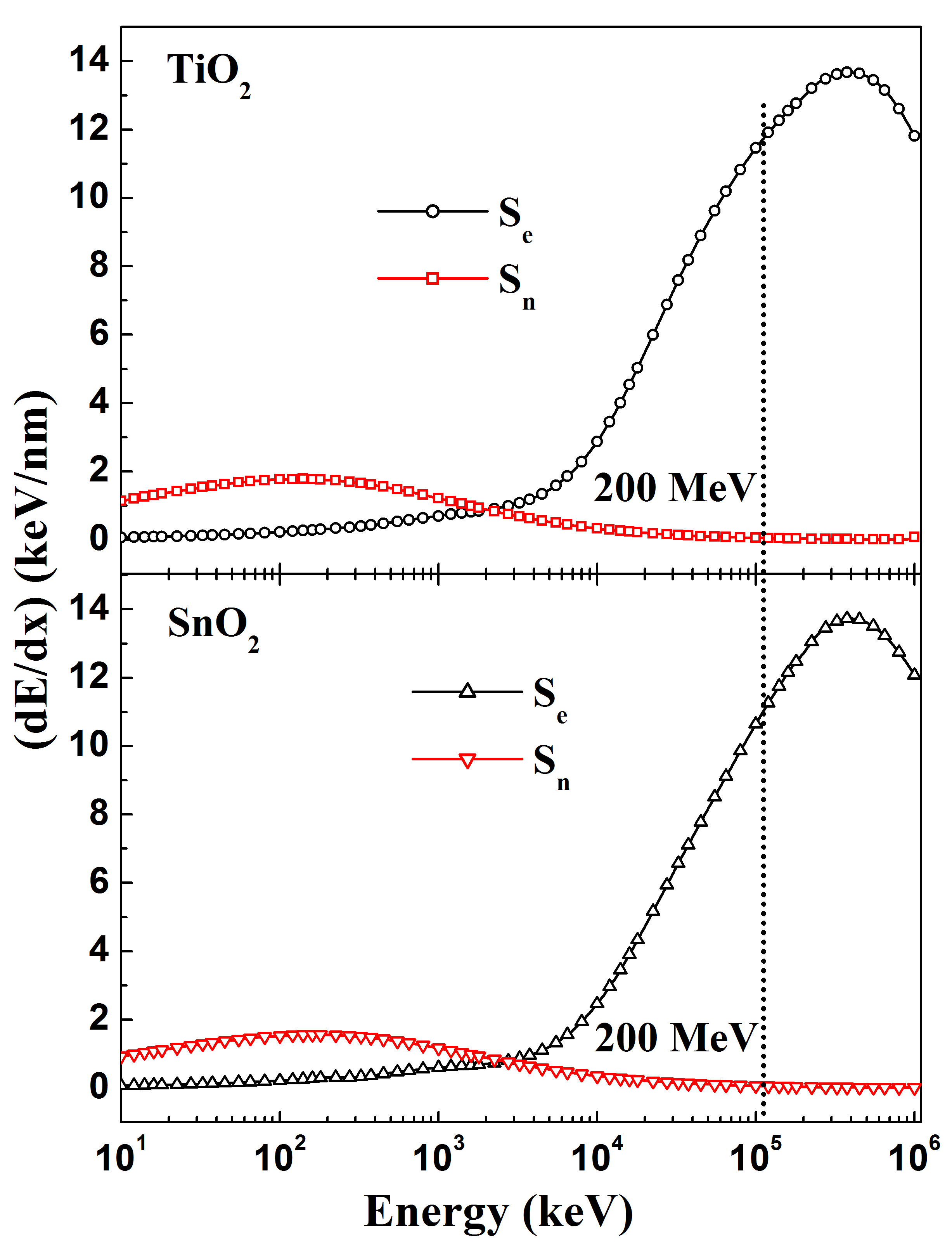
The values of optical absorption edges obtained in our experiments are observed to deviate from the known values reported in the literature r9 ; r24 . The obvious band gap energy changes of both oxide systems indicate the possibility of band gap engineering in the as-deposited thin films by means of SHI irradiation. If the observed modifications in the optical properties are to be understood, an analysis of the possible implications of ion transport through the film is necessary. When 200-MeV Ag15+ ions pass through the oxide films, they loses energy by collisions with nuclei (nuclear stopping power Sn) and inelastic collisions with electrons (electronic stopping power Se). In the present case, for a TiO2 film, S keV/nm and S eV/nm while for a SnO2 film, Se keV/nm and S eV/nm as calculated by using stopping and range of ions in matter software r25 . The vertical line marks a 200-MeV incident ion energy, the energy used in the present work (see Fig. 5). From these values, at higher energies, the electronic energy loss can be seen to dominate the nuclear energy loss, and at an energy of a few hundreds of keV, the opposite is true. Thus, the inelastic electronic collision process is the dominant energy loss mechanism, which induces point and columnar defects and can lead to an increase in the defect density and to a modification in the lattice structure r26 .
III Conclusions
In this study, the transmittance of the TiO2 thin films increased with increasing SHI fluence while the transmittance of the SnO2 thin films decreased. Both oxide systems showed improvements in the transmittance as the irradiation fluence was increased. An anomalous trend was observed for the optical absorption edges with increasing SHI fluence for both the oxide materials. For irradiated TiO2 thin films, the optical band gap values for the indirect transitions were shown to be much higher than the expected values reported. The highest value of the band gap was achieved in the sample SHI-irradiated at a fluence of ions/cm2 while the lowest value of the band gap was observed in the pristine sample. A similar trend was observed in the irradiated SnO2 samples. However, for the irradiated SnO2 thin films, the band gap values on an average decreased.
From the results, we can conclude that SHI does not critically affects the pristine TiO2 samples while for SnO2, significant modifications in the optical properties are observed. These observed changes in the optical properties of both the pristine TiO2 and SnO2 films with SHI fluence can be attributed to controlled structural disorder/defects in the system. Our results show a direct linkage between SHI-induced structural disorder/defects and modifications in the optical properties of the oxide materials.
Acknowledgements.
The authors would like to thank the Inter-University Accelerator Centre, New Delhi, India and the Korea Institute of Science and Technology (KIST, Project No. 2V02631), Seoul, Korea for experimental support. The Department of Science and Technology (DST), Government of India, is acknowledged for supporting this work under Project No. S2/SR/CMP-0051/2007.References
- (1) S. A. Wolf, D. D. Awschalom, R. A. Buhrman, J. M. Daughton, S. von Molánar, M. L. Roukes, A. Y. Chtchelkanova, and D. M. Treger, Science 294, 1488 (2001).
- (2) Y. Matsumoto, M. Murakami, T. Shono, T. Hasegawa, T. Fukumura, M. Kawasaki, P. Ahmet, T. Chikyow, S. -Y. Koshihara, and H. Koinuma, Science 291, 854 (2001).
- (3) A. Fujishima and K. Honda, Nature 238, 37 (1972).
- (4) K. M. Glassford and J. R. Chelikowsky, Phys. Rev. B 46, 1284 (1992).
- (5) M. Ramamoorthy, R. D. King-Smith, and D. Vanderbilt, Phys. Rev. B 49, 7709 (1994).
- (6) P. J. D. Lindan, N. M. Harrison, M. J. Gillan, and J. A. White, Phys. Rev. B 55, 15919 (1997).
- (7) L. Martinu and D. Poitras, J. Vac. Sci. & Tech. A 18, 2619 (2000).
- (8) W. Brown and W. Grannemann, Solid-State Elect. 21, 837 (1978).
- (9) J. -G. Li, T. Ishigaki, and X. Sun, J. Phys. Chem. C 111, 4969 (2007).
- (10) Z. Zhang, C. -C. Wang, R. Zakaria, and J. Y. Ying, J. Phys. Chem. B 102, 10871 (1998).
- (11) M. Law, D. J. Sirbuly, J. C. Johnson, J. Goldberger, R. J. Saykally, and P. Yang, Science 305, 1269 (2004).
- (12) M. S. Arnold, P. Avouris, Z. W. Pan, and Z. L. Wang, J. Phys. Chem. B 107, 659 (2003).
- (13) Y. -S. Hea, J. C. Campbella, R. C. Murphya, M. Arendta, and J. S. Swinneaa, J. Mater. Res. 8, 3131 (1993).
- (14) H. K. Pulker, Surf. Coat. Tech. 112, 250 (1999).
- (15) D. K. Shukla, R. Kumar, S. Mollah, R. J. Choudhary, P. Thakur, S. K. Sharma, N. B. Brookes, and M. Knobel, Phys. Rev. B 82, 174432 (2010).
- (16) H. Thakur, P. Thakur, R. Kumar, N. B. Brookes, K. K. Sharma, A. P. Singh, Y. Kumar, S. Gautam, and K. H. Chae, Appl. Phys. Lett. 98, 192512 (2011).
- (17) H. Thakur, R. Kumar, P. Thakur, N. Brookes, K. Sharma, A. P. Singh, Y. Kumar, S. Gautam, and K. Chae, Chem. Phys. Lett. 511, 322 (2011).
- (18) S. Y. Kim, Appl. Opt. 35, 6703 (1996).
- (19) H. Demiryont, J. R. Sites, and K. Geib, Appl. Opt. 24, 490 (1985).
- (20) N. Daude, C. Gout, and C. Jouanin, Phys. Rev. B 15, 3229 (1977).
- (21) H. Tang, K. Prasad, R. Sanjines, P. E. Schmid, and F. Levy, J. Appl. Phys. 75, 2042 (1994).
- (22) J. Robertson, J. Phys. C 12, 4767 (1979).
- (23) C. Drake and S. Seal, Appl. Phys. Lett. 90, 233117 (2007).
- (24) K. B. Sundaram and G. K. Bhagavat, J. Phys. D: Appl. Phys. 14, 921 (1981).
- (25) J. Biersack and L. Haggmark, Nuclear Instr. Meth. B 174, 257 (1980).
- (26) P. K. Kulriya, B. R. Mehta, D. K. Avasthi, D. C. Agarwal, P. Thakur, N. B. Brookes, A. K. Chawla, and R. Chandra, Appl. Phys. Lett. 96, 053103 (2010).