Surface effects in a semiconductor photonic nanowire and spectral stability of an embedded single quantum dot
Abstract
We evidence the influence of surface effects for \ceInAs quantum dots embedded into \ceGaAs photonic nanowires used as efficient single photon sources. We observe a continuous temporal drift of the emission energy that is an obstacle to resonant quantum optics experiments at the single photon level. We attribute the drift to the sticking of oxygen molecules onto the wire, which modifies the surface charge and hence the electric field seen by the quantum dot. The influence of temperature and excitation laser power on this phenomenon is studied. Most importantly, we demonstrate a proper treatment of the nanowire surface to suppress the drift.
pacs:
78.55.-m,78.67.Uh,85.60.Jb,81.65.-bEfficient nanophotonic devices like single photon sources require to funnel a large fraction of the spontaneous emission (SE) of a single emitter into a single optical mode. This situation offers an ideal platform for quantum optics and quantum information processing experiments Auffèves-Garnier et al. (2007); Englund et al. (2007). In this context, photonic semiconducting nanowires (PW) embedding a single quantum dot (QD) have emerged as appealing systems Friedler et al. (2009); Claudon et al. (2010); Babinec et al. (2010). These monomode waveguides made of a high refractive index material, offer a tight lateral confinement of the guided mode while simultaneously screening all the other transverse modes. Hence they ensure an efficient SE control over a broad wavelength range (90% over a bandwidth exceeding at )Friedler et al. (2009); Bleuse et al. (2011). Moreover the far-field outcoupling efficiency of the guided mode can reach unity by proper engineering of the wire endsFriedler et al. (2009). Following this strategy, an on-demand single-photon source with a record-high brightness was demonstratedClaudon et al. (2010).
However, miniaturization of photonic devices enhances surface effects, inducing for example non radiative surface recombinations which affect the emission properties of semiconducting nanowiresDemichel et al. (2010); Dan et al. (2011). In the case of PWs, single-mode operation imposes a wire diameter , where is the index of refraction of the material. For \ceGaAs PWs the QD is thus located at distances not larger than from sidewalls. It was shown in Ref. 6 that the almost perfect QD radiative yield is preserved in PWs with as small as . Photon correlation experiments showed no bunching in the 1– temporal rangeClaudon et al. (2010), a strong evidence of absence of blinking at this timescale. Nevertheless, the spectral stability of the PWs, crucial for resonant quantum optics experiments, has not been investigated so far. In this letter, we perform high resolution spectroscopy and show that the excitonic emission line of the QD undergoes a continuous energy drift. We discuss the possible origin of the phenomenon, which we attribute to oxygen adsorption on the wire sidewalls, and demonstrate a way to circumvent this problem with a proper surface treatment.
The device fabrication starts from a planar structure grown by molecular beam epitaxy on a \ceGaAs wafer. A single layer of \ceInAs self-assembled QDs (areal density ) is located in a GaAs matrix (residual positive doping ). The ensemble luminescence peaks at ( inhomogeneous broadening). PWs are defined with a top-down approach, using e-beam lithography and dry plasma etching (\ceAr-SiCl4 plasma). A careful control of the etching leads to a conical wire geometry in order to control the optical mode transverse profile along the wire. A series of PWs with top diameters varying by a fine step were fabricated. The actual wire diameter at the dot location is measured with a accuracy by electron microscopy. A wire with a diameter typically contains 10 randomly located QDs. As surface passivation helps in reducing surface effects Dan et al. (2011), we start from the previous device to fabricate surface capped-PWs. The oxide layer is removed by wet chemical etching. \ceGaAs dangling bonds at the surface are saturated by \ce(NH4)2S in order to reduce the density of surface traps. Finally a -thick layer of \ceSi3N4 is deposited over the surface.
The sample is mounted on a cold finger cryostat with optical access. QDs are excited through a 0.75 NA microscope objective. Standard cw diode or Ti:Sa laser excite the QDs. Bandgap (BG) excitation at creates electron-hole pairs in the bulk \ceGaAs matrix. Wetting layer (WL) excitation () only excites carriers in the continuum absorption band of the \ceInAs monolayer close to the QDs. Finally quasi-resonant p-shell excitation () excites discrete QD states. The light emitted by the recombination of the QD lowest energy states is recollected by the same lens and sent to a focal length spectrometer ( spectral resolution at ). A CCD camera is placed at the output of the spectrometer. Its pixel size () corresponds to an energy step comparable to the resolution. Successive QD photoluminescence (PL) spectra are recorded and fitted with a Lorentzian function. Considering the signal to noise ratio for the data, we estimate the statistical uncertainty on the peak position to be .
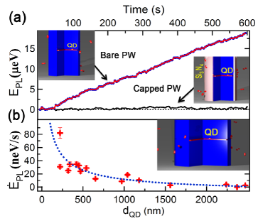
Figure 1(a) presents the PL peak position versus time for a single QD in a bare PW at . The quantum dot is excited by pumping the WL at a power ( is the saturation power of the QD). A regular drift of the emission energy towards higher frequencies is observed (blue drift). A linear fit of the data of Fig. 1(a) gives . At , remains constant over 8 hours. Over this period of time, PL intensity does not change significantly, its linewidth remains limited by the resolution of the spectrometer and lifetime measurements show a small decrease from 1.65 to . Warming up to room temperature and pumping on the cryostat resets the emission energy to its initial lower value. A systematic study of many PWs with different diameters [Fig. 1(b)] reveals that all QDs are affected by a blue drift whose amplitude decreases with increasing diameter. Finally the same experiment with QDs in capped PWs shows no drift (Fig. 1(a), ).
Previous observations clearly point towards surface effects. Dry etching of PWs during their fabrication creates a large density of surface traps Demichel et al. (2010) . For \ceGaAs, the energy of those traps is in the middle of the gap ()Tanaka et al. (2001). If the density of states at this energy is large enough, the Fermi level is pinned and hence the energy bands are bended close to the surface. Band bending is accompanied by a surface built-in electric field and a positive charging of the surface for p-doped semiconductors. Assuming a planar interface, the depletion length over which the bands are shifted is , where is the dielectric constant of \ceGaAs, the vacuum permittivity and the electron charge. For , (). Hence the region of the PW containing the dots is fully depleted and an electric field is present over its entire cross-section, explaining why all studied QDs experience a drift. We have confirmed this fact with numerical simulations. It shows that the field inside the wire is proportional to the surface charge. Due to the conical shape of the PW a small and almost constant component of the electric field exists along the axis of the wire. The radial electric field ranges from on the PW axis to at the surface. An embedded \ceInAs QD subjected to this field experiences a Stark energy shift Fry et al. (2000); Gerardot et al. (2007) , with and . We note that a blue drift implies a reduction of the electric field, hence a diminution of the positive net charge at the surface of the PW.
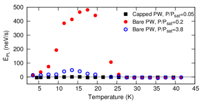
We attribute this effect to the physisorption of \ceO2 onto the surface leading to the creation of acceptor-like surface states that capture one electron Chen et al. (1991); Nienhaus and Mönch (1993); Anderson et al. (1990). The reset of to a low value after warming up to room temperature implies a reversible physical phenomenon and not an irreversible chemical surface reaction. The full circles on Fig. 2 represent the dependence of as a function of between 4 and in the same conditions as in Fig. 1(a). A ten-fold increase occurs from 4 to before the drift dramatically drops to values very close to 0 above . This observation is in good agreement with previous studies on the adsorption of \ceO2 on \ceGaAs, which evidenced an adsorption peak around Honig and Hook (1960); Anderson et al. (1990). The same experiment for a capped PW (full squares in Fig. 2) shows that remains below over the whole temperature range, proving the drift cancellation by the capping. The temperature dependence of under high excitation power (3.8; open circles in Fig. 2) exhibits the same characteristic peak. Its maximum value is shifted to lower temperature by and is dramatically smaller than for low power excitation. The pump laser can affect the PW in different ways: it can locally warm up the PW (explaining in particular the peak shift at high power in Fig. 2), photocreated carriers can screen the electric field Tanaka et al. (2001) or change the adsorption rate of \ceO_2.
To better understand the phenomenon, we performed systematic power studies at . Figure 3(a) presents a typical experimental run: the drift is determined from measurement of the emission energy over at different power values. Here, we also observe sudden shifts of the emission energy when the power is increased. We attribute it to a local warming of the PW () leading to the usual quadratic shift of the bandgap. For p-shell excitation, the amplitude of is below the fitting uncertainty on the peak position (). In the other two cases, increases linearly with power. Its magnitude is larger for BG excitation compared to WL excitation. Similar values have been observed for many QDs in PWs of similar size, capped or not.
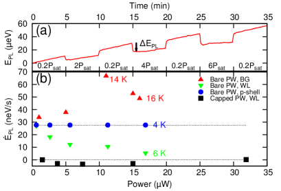
The influence of power on crucially depends on the excitation conditions (see Fig. 3(b)). For p-shell excitation, where no free carrier is injected in the PW and no heating is generated, it remains constant. In the case of WL excitation, where remains below , one observes a decrease of . On the other hand for BG excitation, at high power is close to the maximum drift temperature of Fig. 2. This explains why we observe an increase of , which is dominated by temperature effect. However it is worth noting that its maximum value is 7 times lower than the one predicted by the low excitation results of Fig. 2. Hence it is legitimate to think that, as in the case of WL excitation, the effect of temperature is strongly inhibited by an increase of excitation power. A possible explanation for our observations is the presence of photocreated carriers that screen the surface built-in electric field. This phenomenon should lead to a dramatic reduction of the electric field seen by the QD and hence induce a blue shift of its emission energy. This is in direct contradiction with the results of Fig. 3(a). A another explanation that remains to be confirmed could be a direct influence of the carriers or excitation light on the dynamics of adsorption and desorption of \ceO2 or on its capture of an electron.
The power dependence of for capped PWs is given in Fig. 3(b) and is consistent with a complete suppression of the drift. Although there may still exist a static electric field inside the PW due to surface states at the \ceGaAs/\ceSi3N4 interface, its value is frozen and no longer depends on the adsorption of molecules on the device. Frequency stability of the emission of a single QD is crucial to perform high precision resonant spectroscopic studies. In our device, the QD now behaves as a stable two-level system embedded into an optical waveguide made by the PW. It is an ideal situation for studying non-linear effects at the single photon level and implementing simple quantum information operation between light and a solid state emitterAuffèves-Garnier et al. (2007).
We acknowledge fruitful discussions with O. Demichel and M. Richard. This work is supported by ANR (P3N project CAFE) and by fundation “Nanosciences aux limites de la Nanoélectronique”. Sample fabrication was done in the PTA and CEA LETI MINATEC/DOPT clean rooms.
References
- Auffèves-Garnier et al. (2007) A. Auffèves-Garnier, C. Simon, J.-M. Gérard, and J.-P. Poizat, Phys. Rev. A 75, 053823 (2007).
- Englund et al. (2007) D. Englund, A. Faraon, I. Fushman, N. Stoltz, P. Petroff, and J. Vuckovic, Nature 450, 857 (2007).
- Friedler et al. (2009) I. Friedler, C. Sauvan, J. P. Hugonin, P. Lalanne, J. Claudon, and J. M. Gérard, Opt. Express 17, 2095 (2009).
- Claudon et al. (2010) J. Claudon, J. Bleuse, N. S. Malik, M. Bazin, P. Jaffrennou, N. Gregersen, C. Sauvan, P. Lalanne, and J.-M. Gérard, Nat Photon 4, 174 (2010).
- Babinec et al. (2010) T. M. Babinec, H. J. M., M. Khan, Y. Zhang, J. R. Maze, P. R. Hemmer, and M. Loncar, Nat Nano 5, 195 (2010).
- Bleuse et al. (2011) J. Bleuse, J. Claudon, M. Creasey, N. S. Malik, J.-M. Gérard, I. Maksymov, J.-P. Hugonin, and P. Lalanne, Phys. Rev. Lett. 106, 103601 (2011).
- Demichel et al. (2010) O. Demichel, M. Heiss, J. Bleuse, H. Mariette, and A. F. i Morral, Appl. Phys. Lett. 97, 201907 (2010).
- Dan et al. (2011) Y. Dan, K. Seo, K. Takei, J. H. Meza, A. Javey, and K. B. Crozier, Nano Letters 11, 2527 (2011).
- Tanaka et al. (2001) S. Tanaka, S. D. More, J. Murakami, M. Itoh, Y. Fujii, and M. Kamada, Phys. Rev. B 64, 155308 (2001).
- Fry et al. (2000) P. W. Fry, I. E. Itskevich, D. J. Mowbray, M. S. Skolnick, J. J. Finley, J. A. Barker, E. P. O’Reilly, L. R. Wilson, I. A. Larkin, P. A. Maksym, M. Hopkinson, M. Al-Khafaji, J. P. R. David, A. G. Cullis, G. Hill, and J. C. Clark, Phys. Rev. Lett. 84, 733 (2000).
- Gerardot et al. (2007) B. D. Gerardot, S. Seidl, P. A. Dalgarno, R. J. Warburton, D. Granados, J. M. Garcia, K. Kowalik, O. Krebs, K. Karrai, A. Badolato, and P. M. Petroff, Appl. Phys. Lett. 90, 041101 (2007).
- Chen et al. (1991) Y. Chen, F. Stepniak, J. M. Seo, S. E. Harvey, and J. H. Weaver, Phys. Rev. B 43, 12086 (1991).
- Nienhaus and Mönch (1993) H. Nienhaus and W. Mönch, Appl. Surf. Sci. 65, 632 (1993).
- Anderson et al. (1990) S. G. Anderson, T. Komeda, J. M. Seo, C. Capasso, G. D. Waddill, P. J. Benning, and J. H. Weaver, Phys. Rev. B 42, 5082 (1990).
- Honig and Hook (1960) R. E. Honig and R. O. Hook, RCA Rev. 21, 360 (1960).