Ultra-shallow quantum dots in an undoped GaAs/AlGaAs 2D electron gas
Abstract
We report quantum dots fabricated on very shallow 2-dimensional electron gases, only 30 nm below the surface, in undoped GaAs/AlGaAs heterostuctures grown by molecular beam epitaxy. Due to the absence of dopants, an improvement of more than one order of magnitude in mobility (at 21011 cm-2) with respect to doped heterostructures with similar depths is observed. These undoped wafers can easily be gated with surface metallic gates patterned by e-beam lithography, as demonstrated here from single-level transport through a quantum dot showing large charging energies (up to 1.75 meV) and excited state energies (up to 0.5 meV).
Electrostatically-defined quantum dots fabricated on high-mobility GaAs/AlGaAs heterostructure have been and continue to be invaluable in many fundamental investigations, e.g. Kondo physics and spin-based solid-state qubits. Unfortunately, the characteristics of these devices are extremely sensitive to seemingly random charge fluctuations in their local electrostatic potential, commonly known as Random Telegraph Signal (RTS) noise, or charge noise. Although one can perform a biased coolingPioro-Ladriere et al. (2005); Buizert et al. (2008) or a thermal cureFujiwara et al. (2002) to attempt to drastically reduce the levels of charge noise on a given device, results from both techniques vary from device to device.
Quantum dots fabricated in shallow two-dimensional electron gases (2DEGs) have two advantages over their deeper cousins. First, finer features can be transferred from the surface metallic gates to the 2DEG. Second, the energy scales of the dot levels tends to be larger, which enable operation at higher temperatures. However, shallow 2DEG depths (as little as 20 nm below the surface) come at the expense of mobility.Kopnov et al. (2010); Laroche et al. (2010); Giesbers et al. (2010); Rossler et al. (2010a); Nemutudi et al. (2005); Gildemeister et al. (2007); Nakamura et al. (2010); Mühle et al. (2008); Fricke et al. (2007); Nemutudi et al. (2004); Goldhaber-Gordon et al. (1998) Furthermore, the dopant layer may partially screen surface gates (through hopping conduction) and/or facilitate gate leakage, rendering many such wafers ungateable by surface metallic gates. The ungateability of some doped wafers is not only restricted to shallow 2DEGs, but also can occur in high-mobility doped wafers.Miller et al. (2007); Dolev et al. (2008); Rossler et al. (2010b)
The limitations described above can be circumvented or mitigated by using undoped heterostructures in different field-effect transistor (FET) geometries such as the SISFETKane et al. (1993); Kawaharazuka et al. (2001); Reilly et al. (2002); Noh et al. (2003); Lilly et al. (2003) (semiconductor-insulator-semiconductor), the MISFETHerfort and Hirayama (1996); Harrell et al. (1999); Willett et al. (2006) (metal-insulator-semiconductor), or the HIGFET111The term HIGFET has been used in the literature to refer to both SISFET and/or MISFET geometries. By MISFET, we mean the gate is a metal (e.g. Au) and the insulator is some dielectric. By SISFET, we mean the gate is a highly-doped semiconductor (metallic regime) and the insulator is also a semiconductor. (heterostructure-insulator-gate). Since there are no intentional dopants, the 2DEG can be brought much closer to the surface without sacrificing mobility. Furthermore, undoped quantum dots would not suffer from one possible source of charge noise: electrons hopping between dopant sites in AlGaAs. In doped wafers, intentional dopants typically outnumber unintentional dopants 10,000 to 1 (depending on mobility). Finally, undoped quantum dots may also interact with fewer undesirable impurities in the vicinity and are far more reproducible upon thermal cycling than their doped counterparts.See et al. (2012) In this Letter, we compare ultra-shallow undoped and doped GaAs/AlGaAs 2DEGs, and demonstrate gated quantum dots on ultra-shallow undoped heterostructures.
Three undoped heterostructures were grown on the same day (V625, V626, and V627) with their MBE layers shown in Figure 1(a). Details of fabrication are otherwise identical to and extensively described in Ref. Mak et al., 2010. The surface Ti/Au gates defining our quantum dots were fabricated by e-beam lithography directly on the surface of the GaAs cap, below the insulator layer (500 nm of polyimide, or 175 nm of SiO2). Above the insulator layer, a Ti/Au overall topgate covers the entire surface of the 2DEG (overlapping the ohmic contacts) and varies the carrier density. Measurements were performed in a pumped-3He cryostat.


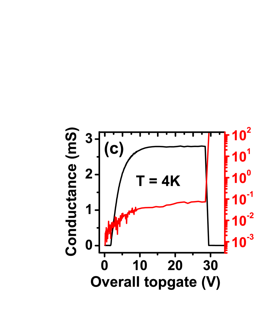
The typical failure mechanism in SISFETs and MISFETs are electrical shorts between the ohmic contacts and the overall topgate.Sarkozy et al. (2007) None of our samples suffered from this problem. Indeed, the relationship between density and the overall topgate voltage is linear for V625 and V627 [Fig. 1(b)], and the carrier density does not saturate with overall topgate voltage. Both observations are consistent with no leakage from the overall topgate to the 2DEG [Fig. 1(c)]. However, we found that in V626 the AlGaAs barrier was not insulating enough to prevent charge leaking between the 2DEG and the semiconductor-insulator interface (a GaAs-polyimide interface in our case). Shortly after the 2DEG is fully induced, charge “seeps” through the AlGaAs barrier. As it gradually accumulates at the GaAs-polyimide interface, it begins to screen the overall topgate from the 2DEG, which results in a gradual loss of carriers until the 2DEG pinches off with time.222The timescale for this process is of order of a several minutes, with factors being the resistance and capacitance across the AlGaAs barrier (thus determining an time constant), and the speed at which the overall topgate is ramped (or if held steady). In this scenario, we emphasize that no leakage is observed between the 2DEG and the overall topgate: no current flows through the insulating polyimide layer. In V627, increasing the energy height of the AlxGa1-xAs barrier (by using = 0.90 instead of = 0.33) eliminated the “seeping” leak between the 2DEG and the GaAs-polyimide interface. The ultra-shallow 2DEG in V627 was stable in time and did not leak to the overall topgate [Fig. 1(c)], and neither do any of our deeper undoped 2DEGs.


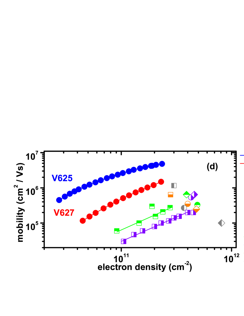
Figure 1(d) compares 2D transport characteristics between shallow GaAs/AlGaAs 2DEGs from our undoped wafers and from a representative sample of published values of doped wafers. The large improvement in mobility (more than one order of magnitude at 21011 cm-2) is largely attributable to the absence of intentional dopants. Although scattering due to surface states is significant for a 2DEG depth less than 80 nm from the surface,Mak et al. (2010) it is still by far the scattering from remote ionized impurities that impairs mobility in doped shallow 2DEG wafers.Gold (1988); MacLeod et al. (2009) The difference in mobility between V625 and V627 is mostly accounted for by surface states which we simulated as a delta-doped layer at the surface for the purposes of scattering.Mak et al. (2010)
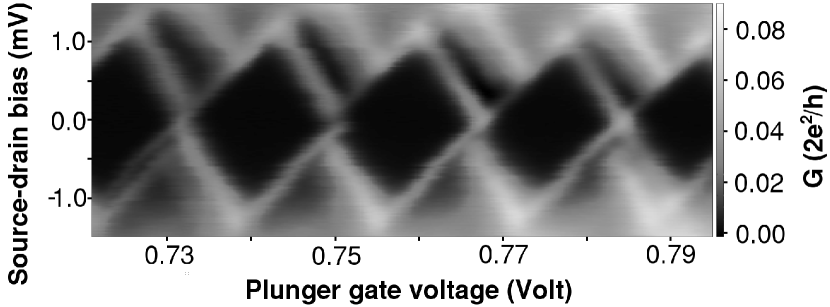
It is only recently that quantum dots have been fabricated in undoped heterostructures with electronsSee et al. (2010) and holes.Klochan et al. (2010) No RTS event could be observed in the electron quantum dot fabricated on the SISFET of Ref. [See et al., 2010]. Figure 2 shows Coulomb blockade (CB) oscillations in the weak coupling regime from one of three quantums dot fabricated on wafer V627 (the other two devices have similar characteristics as those shown here). The surfaces gates defining the quantum dot [Fig. 2(a)] do not leak significantly below 0.95V [Fig. 2(b)]. Our typical leakage current is 10-20 pA, the effective sensitivity floor of our measurement setup. All surface gate voltages are positive: they partially screen the overall topgate and thus require a positive bias to help the overall topgate induce a 2DEG at the center of the quantum dot. Directly underneath the surface gates, the electric field from the overall topgate is totally screened and a 2DEG does not form until a much higher positive voltage is applied to the surface gates.
Despite its large dimensions, the charging energy ( = , where the total capacitance) of our our quantum dot is rather large: = 1.25 meV [Fig. 3]. By suitably changing gate voltages, can be tuned as high as 1.75 meV, but the dot is then no longer in the weak coupling regime. The (weak coupling regime) charging energy in our MISFET ( = 1.25 meV) is larger than that ( = 0.5 meV) of the quantum dot on the SISFET from Ref. [See et al., 2010]. The single-particle energy level spacing () of our quantum dot is also larger, 0.5 meV as opposed to 0.2 meV, and enables the observation of excited states at 400 mK. The total capacitance of our MISFET dot (128 aF) is slightly less than that of the SISFET dot (160 aF), and is dominated by the capacitance to the large overall topgate above the quantum dot in both cases. Using the 2D electron density and the area implied by the measured total capacitance (assuming = ), there are at most 80 electrons in our dot. The energy scales of and are directly related to the 2DEG depths of the SISFET (185 nm deep) and our MISFET (30 nm deep). Using = and the values above, we estimate a quantum dot fabricated on a hypothetical SISFET with a 30 nm deep 2DEG would have a large total capacitance, 800 aF. It therefore appears more advantageous to fabricate quantum dots from MISFETs rather than SISFETs.


At finite temperature , the conductance through a quantum dot is determined by:Foxman et al. (1994)
| (1) | |||||
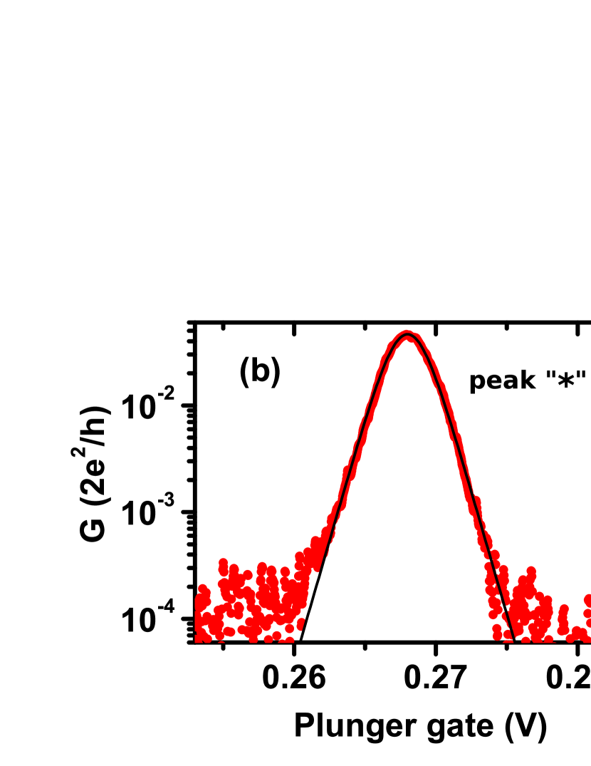
where is a constant, the chemical potential, the Boltzmann constant, and is the average of the tunneling rates through the left and right barriers of the quantum dot. If the dot is strongly coupled to the leads (), the CB peak lineshape is a Lorentzian [ 0.35 V in Fig. 1]. In the weak coupling regime, if transport through the dot involves only a single energy level and is very small (), then the lineshape of the CB conductance peak can be approximated by:Foxman et al. (1993); Beenakker (1991)
| (2) |
where is a constant, the lever arm of the plunger gate, the plunger gate voltage, and the plunger voltage at the center of the CB peak. If more than one energy level is involved in transport (), then the following approximation can be used:Foxman et al. (1994); Beenakker (1991)
| (3) |
where is a constant and is the single-particle energy level spacing.
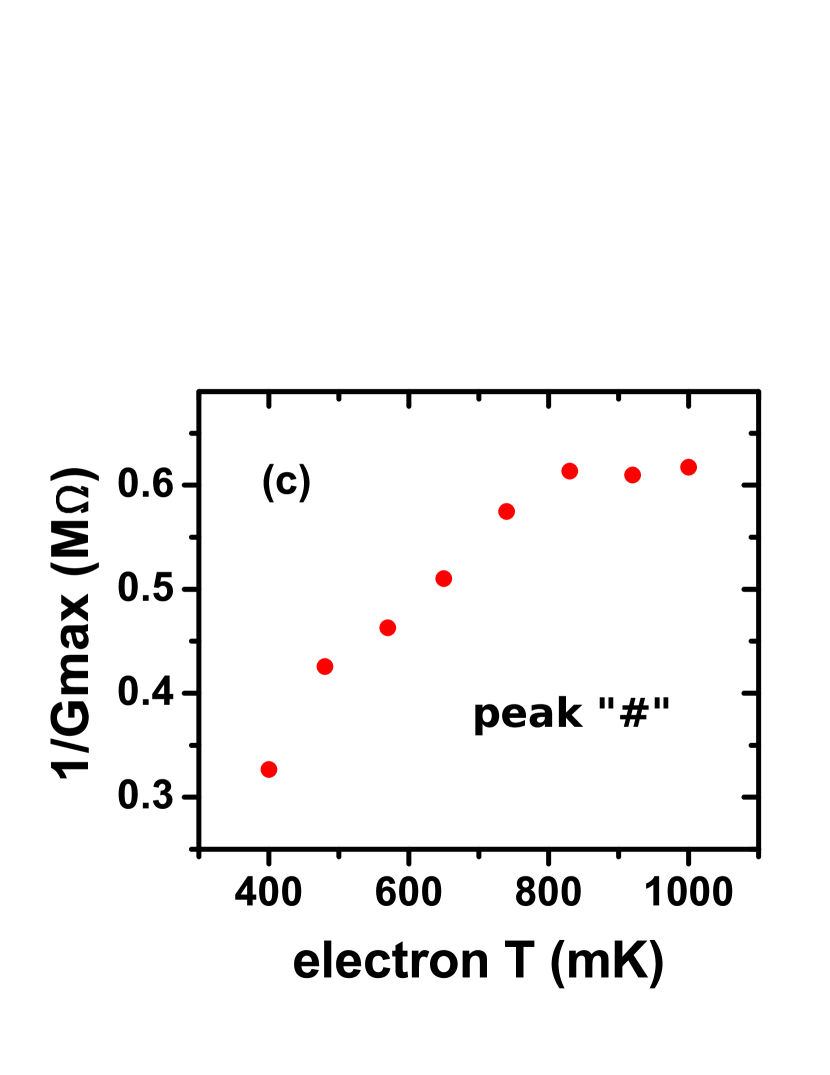
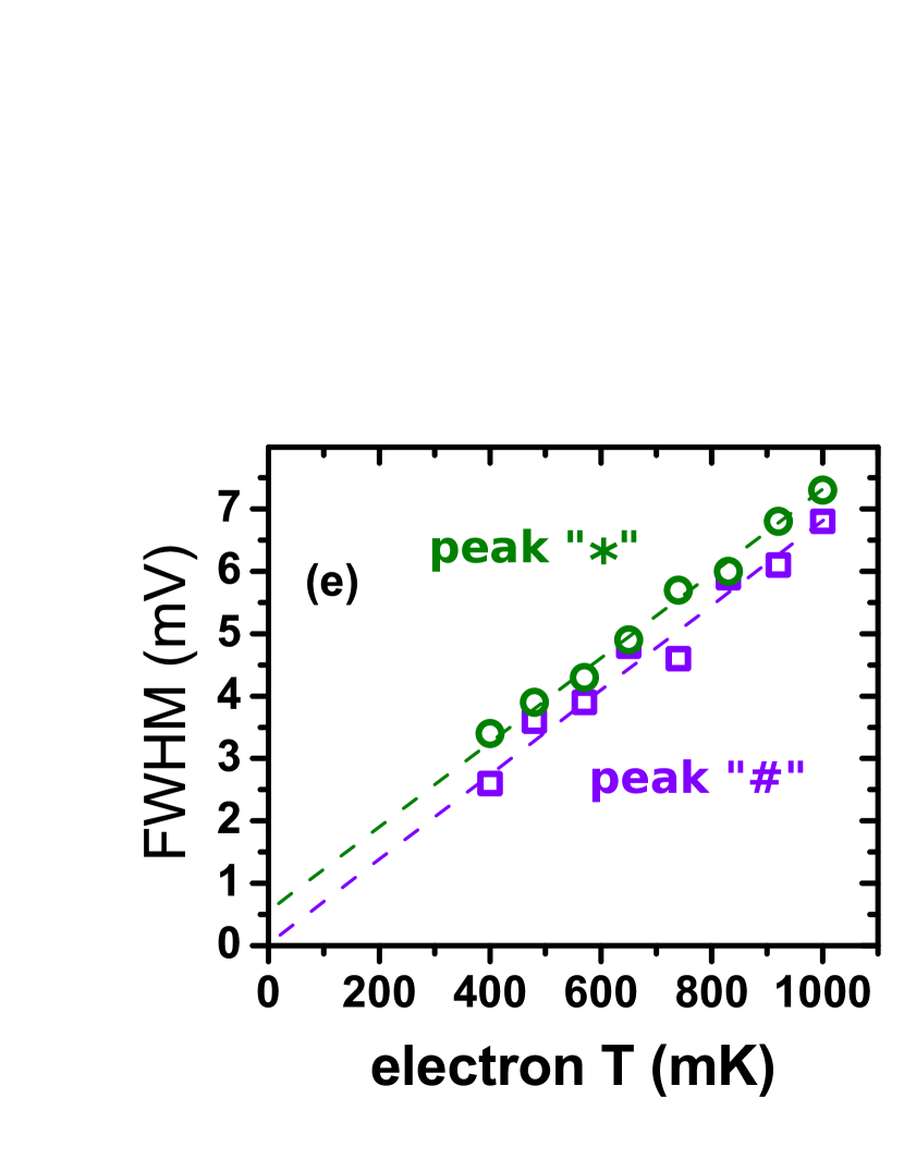
Figure 4 shows the analysis of the temperature dependence of the CB peaks labeled “” and “” in Figure 2. Both peaks fit the lineshape generated by equation (2) [Figs. 4(a) and 4(b)]. This, combined with the linear temperature dependence of the inverse of the maximum CB peak height (1/Gmax) in Figs. 4(c) and 4(d), strongly suggest single-level transport occurs at temperatures below 800 mK. Above 800 mK, 1/Gmax becomes independent of temperature, signalling a transition from single-level transport () to multi-level transport () through the quantum dot. The FWHM of both peaks linearly increases with temperature in both regimes [Fig. 4(e)].
When extrapolated to =0, the FWHM of peak “” [Fig. 4(e)] is zero, consistent with the approximation , used to derive Eqn. (2). Similarly, 1/Gmax goes to zero at =0 [Fig. 4(c)]. The story is different for peak “”. When extrapolated to =0, its FWHM reads the finite value 0.5 mV in gate voltage units which, when converted to energy units (using eV/mV), gives eV, a measure of the lifetime broadening of this energy level. This is roughly half our base electron temperature. Thus, although Eqn. (2) does not strictly apply, the single-level transport regime is still accessible (because ). That for peak “” also explains the presence of a finite offset at for 1/Gmax in Fig. 4(d). Stated otherwise, Gmax does not blow up to infinity at T=0, but remains finite. This behavior is well understood.Foxman et al. (1994)
In conclusion, we have shown ultra-shallow 2DEGs (within 30 nm of the surface) in undoped GaAs/AlGaAs heterostructures that display no parallel conduction, are gateable, and show no hysteresis upon gate action. The absence of dopants has improved their mobility by more than one order of magnitude relative to their doped counterparts with similar 2DEG depths and carrier densities. We have also demonstrated that these undoped heterostructures can be used to fabricate single-electron quantum dots defined by surface metal gates, with charging energies of up to 1.75 meV and excited state energies of up to 0.5 meV.
The authors would like to thank S.J. Chorley and C.J.B. Ford for their help, and acknowledge financial support from Toshiba Research Europe and the EPSRC.
References
- Pioro-Ladriere et al. (2005) M. Pioro-Ladriere, J. H. Davies, A. R. Long, A. S. Sachrajda, L. Gaudreau, P. Zawadzki, J. Lapointe, J. Gupta, Z. Wasilewski, and S. Studenikin, Phys. Rev. B 72, 115331 (2005).
- Buizert et al. (2008) C. Buizert, F. H. L. Koppens, M. Pioro-Ladriere, H. P. Tranitz, I. T. Vink, S. Tarucha, W. Wegscheider, and L. M. K. Vandersypen, Phys. Rev. Lett. 101, 226603 (2008).
- Fujiwara et al. (2002) M. Fujiwara, M. Sasaki, and M. Akiba, Appl. Phys. Lett. 80, 1844 (2002).
- Kopnov et al. (2010) G. Kopnov, V. Y. Umansky, H. Cohen, D. Shahar, and R. Naaman, Phys. Rev. B 81, 045316 (2010).
- Laroche et al. (2010) D. Laroche, S. Das Sarma, G. Gervais, M. P. Lilly, and J. L. Reno, Appl. Phys. Lett. 96, 162112 (2010).
- Giesbers et al. (2010) A. J. M. Giesbers, U. Zeitler, M. I. Katsnelson, D. Reuter, A. D. Wieck, G. Biasiol, L. Sorba, and J. C. Maan, Nature Phys. 6, 173 (2010).
- Rossler et al. (2010a) C. Rossler, B. Küng, S. Drüscher, T. Choi, T. Ihn, K. Ensslin, and M. Beck, Appl. Phys. Lett. 97, 152109 (2010a).
- Nemutudi et al. (2005) R. Nemutudi, C.-T. Liang, M. J. Murphy, H. E. Beere, C. G. Smith, D. A. Ritchie, M. Pepper, and G. A. C. Jones, Microelectronics Journal 36, 425 (2005).
- Gildemeister et al. (2007) A. E. Gildemeister, T. Ihn, R. Schleser, K. Ensslin, D. C. Driscoll, and A. C. Gossard, J. Appl. Phys. 102, 083703 (2007).
- Nakamura et al. (2010) S. Nakamura, Y. Yamauchi, M. Hashisaka, K. Chida, K. Kobayashi, T. Ono, R. Leturcq, K. Ensslin, K. Saito, Y. Utsumi, and A. C. Gossard, Phys. Rev. Lett. 104, 080602 (2010).
- Mühle et al. (2008) A. Mühle, W. Wegscheider, and R. J. Haug, Appl. Phys. Lett. 92, 013126 (2008).
- Fricke et al. (2007) C. Fricke, F. Hohls, W. Wegscheider, and R. J. Haug, Phys. Rev. B 76, 155307 (2007).
- Nemutudi et al. (2004) R. Nemutudi, M. Kataoka, C. J. B. Ford, N. J. Appleyard, M. Pepper, D. A. Ritchie, and G. A. C. Jones, J. Appl. Phys. 95, 2557 (2004).
- Goldhaber-Gordon et al. (1998) D. Goldhaber-Gordon, H. Shtrikman, D. Mahalu, D. Abusch-Magder, U. Meirav, and M. A. Kastner, Nature 391, 156 (1998).
- Miller et al. (2007) J. B. Miller, I. P. Radu, D. M. Zumbuhl, E. M. Levenson-Falk, M. A. Kastner, C. M. Marcus, L. N. Pfeiffer, and K. W. West, Nature Phys. 3, 561 (2007).
- Dolev et al. (2008) M. Dolev, M. Heiblum, V. Umansky, A. Stern, and D. Mahalu, Nature 452, 829 (2008).
- Rossler et al. (2010b) C. Rossler, T. Feil, P. Mensch, T. Ihn, K. Ensslin, D. Schuh, and W. Wegscheider, New J. Phys. 12, 043007 (2010b).
- Kane et al. (1993) B. E. Kane, L. N. Pfeiffer, K. W. West, and C. K. Harnett, Appl. Phys. Lett. 63, 2132 (1993).
- Kawaharazuka et al. (2001) A. Kawaharazuka, T. Saku, C. A. Kikuchi, Y. Horikoshi, and Y. Hirayama, Phys. Rev. B 63, 245309 (2001).
- Reilly et al. (2002) D. J. Reilly, T. M. Buehler, J. L. OBrien, A. R. Hamilton, A. S. Dzurak, R. G. Clark, B. E. Kane, L. N. Pfeiffer, and K. W. West, Phys. Rev. Lett. 89, 246801 (2002).
- Noh et al. (2003) H. Noh, M. P. Lilly, D. C. Tsui, J. A. Simmons, E. H. Hwang, S. Das Sarma, L. N. Pfeiffer, and K. W. West, Phys. Rev. B 68, 165308 (2003).
- Lilly et al. (2003) M. P. Lilly, J. L. Reno, J. A. Simmons, I. B. Spielman, J. P. Eisenstein, L. N. Pfeiffer, and K. W. West, Phys. Rev. Lett. 90, 056806 (2003).
- Herfort and Hirayama (1996) J. Herfort and Y. Hirayama, Appl. Phys. Lett. 69, 3360 (1996).
- Harrell et al. (1999) R. H. Harrell, K. S. Pyshkin, M. Y. Simmons, D. A. Ritchie, C. J. B. Ford, G. A. C. Jones, and M. Pepper, Appl. Phys. Lett. 74, 2328 (1999).
- Willett et al. (2006) R. L. Willett, L. N. Pfeiffer, and K. W. West, Appl. Phys. Lett. 89, 242107 (2006).
- Note (1) The term HIGFET has been used in the literature to refer to both SISFET and/or MISFET geometries. By MISFET, we mean the gate is a metal (e.g. Au) and the insulator is some dielectric. By SISFET, we mean the gate is a highly-doped semiconductor (metallic regime) and the insulator is also a semiconductor.
- See et al. (2012) A. M. See, I. Pilgrim, B. C. Scannell, R. D. Montgomery, O. Klochan, A. M. Burke, M. Aagesen, P. E. Lindelof, I. Farrer, D. A. Ritchie, R. P. Taylor, A. R. Hamilton, and A. P. Micolich, Phys. Rev. Lett. 108, 196807 (2012).
- Mak et al. (2010) W. Y. Mak, K. D. Gupta, H. E. Beere, I. Farrer, F. Sfigakis, and D. A. Ritchie, Appl. Phys. Lett. 97, 242107 (2010).
- Sarkozy et al. (2007) S. Sarkozy, K. D. Gupta, F. Sfigakis, I. Farrer, H. E. Beere, R. Harrell, D. A. Ritchie, and G. A. C. Jones, Electrochemical Soc Proc. 11, 75 (2007).
- Note (2) The timescale for this process is of order of a several minutes, with factors being the resistance and capacitance across the AlGaAs barrier (thus determining an time constant), and the speed at which the overall topgate is ramped (or if held steady). In this scenario, we emphasize that no leakage is observed between the 2DEG and the overall topgate: no current flows through the insulating polyimide layer.
- Gold (1988) A. Gold, Phys. Rev. B 38, 10798 (1988).
- MacLeod et al. (2009) S. J. MacLeod, K. Chan, T. P. Martin, A. R. Hamilton, A. See, A. P. Micolich, M. Aagesen, and P. E. Lindelof, Phys. Rev. B 80, 035310 (2009).
- See et al. (2010) A. M. See, O. Klochan, A. R. Hamilton, A. P. Micolich, M. Aagesen, and P. E. Lindelof, Appl. Phys. Lett. 96, 112104 (2010).
- Klochan et al. (2010) O. Klochan, J. C. H. Chen, A. P. Micolich, A. R. Hamilton, K. Muraki, and Y. Hirayama, Appl. Phys. Lett. 96, 092103 (2010).
- Foxman et al. (1994) E. B. Foxman, U. Meirav, P. L. McEuen, M. A. Kastner, O. Klein, P. A. Belk, D. M. Abusch, and S. J. Wind, Phys. Rev. B 50, 14193 (1994).
- Foxman et al. (1993) E. B. Foxman, P. L. McEuen, U. Meirav, N. S. Wingreen, Y. Meir, P. A. Belk, N. R. Belk, M. A. Kastner, and S. J. Wind, Phys. Rev. B 47, 10020 (1993).
- Beenakker (1991) C. W. J. Beenakker, Phys. Rev. B 44, 1646 (1991).