Efficient photon detection from color centers in a diamond optical waveguide
Abstract
A common limitation of experiments using color centers in diamond is the poor photon collection efficiency of microscope objectives due to refraction at the diamond interface. We present a simple and effective technique to detect a large fraction of photons emitted by color centers within a planar diamond sample by detecting light that is guided to the edges of the diamond via total internal reflection. We describe a prototype device using this “side-collection” technique, which provides photon collection efficiency and photon detection efficiency . We apply the enhanced signal-to-noise ratio gained from side-collection to AC magnetometry using ensembles of nitrogen-vacancy (NV) color centers, and demonstrate AC magnetic field sensitivity , limited by added noise in the prototype side-collection device. Technical optimization should allow significant further improvements in photon collection and detection efficiency as well as sub-picotesla NV-diamond magnetic field sensitivity using the side-collection technique.
pacs:
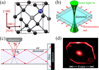
42.79.Gn, 07.55.Ge, 76.30.Mi, 78.55.-mA wide variety of fluorescent point defect centers in diamond have been identified, with possible applications toward quantum information and biological imaging.Aharonovich et al. (2011) One such color center that has attracted considerable attention is the negatively-charged nitrogen-vacancy center (NV) [Fig. 1(a)], which has an electronic structure that allows for optical initialization and detection of the electronic spin, and coherent manipulation of the spin state, Jelezko et al. (2004) with long room-temperature spin coherence times.Balasubramanian et al. (2009) Demonstrated applications of NVs include single photon generation,Beveratos et al. (2001); Babinec et al. (2010) quantum information processing, Dutt et al. (2007); Jiang et al. (2009); Togan et al. (2010) super-resolution microscopy,Rittweger et al. (2009); Maurer et al. (2010) nanoscale magnetometry using a single NV, Maze et al. (2008); Balasubramanian et al. (2008) and vector magnetic field imaging using ensembles of NVs.Pham et al. (2011) For all of these applications, the photon collection efficiency is critically important.
Conventionally, photons emitted from NVs in a bulk diamond substrate are collected using a microscope objective with a large numerical aperture (NA). However, refraction at the flat diamond interface reduces the effective NA of the objective by a factor equal to the refractive index of diamond (), resulting in a photon collection efficiency () .Sup Photon detection efficiencies () are typical when detector coupling and quantum efficiencies are taken into account.
We note that NVs in diamond nanostructures can avoid the -degradation caused by a bulk diamond interface. For example, NVs in subwavelength-size diamond nanocrystals can be approximated as point emitters in the medium surrounding the nanocrystal, yielding higher but lower emission rates due to increased excited state lifetime.Beveratos et al. (2001) Light from NVs inside fabricated diamond nanowires is primarily emitted along the nanowire symmetry axis, allowing .Babinec et al. (2010) However, NVs in diamond nanostructures typically have much shorter spin coherence times Tisler et al. (2009) than those in bulk diamond.Balasubramanian et al. (2009); Stanwix et al. (2010) One approach to increase for NVs in bulk diamond is to construct a solid-immersion lens (SIL) out of the diamond substrate, using either macroscopic Siyushev et al. (2010) or microscopic Hadden et al. (2010) fabrication techniques. Light from NVs at the center of a hemispherical diamond SIL passes through the surface at normal incidence, allowing . However, this improved photon collection efficiency is limited to NVs lying from the center of a macroscopic SIL.Siyushev et al. (2010) For a larger field of view, or for large-volume ensemble measurements in bulk diamond, a different collection-enhancement technique is required.
Here we demonstrate an efficient fluorescence detection technique that uses the planar diamond chip containing the color centers as an optical waveguide. For this “side-collection” technique, photons emitted by the color centers are confined between the two parallel diamond chip surfaces by total internal reflection (TIR) and guided to the sides (edges) of the diamond chip, where they pass through a filter onto a detector [Fig. 1(b,c)]. This technique avoids complicated fabrication procedures and allows efficient photon detection from color centers located anywhere within the diamond volume.
We estimated the expected efficiency of the side-collection technique using theoretical models of the average NV emission pattern and realistic approximations of the diamond chip geometry and acceptance angles of the detectors.Sup We find that of the NV fluorescence is confined by TIR between the polished (100) planar surfaces of the diamond chip, and reaches the detectors on first incidence of the photons with the diamond chip sides (edges). Much of the light also undergoes TIR off the sides, but may reach the detectors after many reflections within the diamond. We therefore expect for the side-collection technique, depending on details of the experimental geometry, diamond chip surface properties, etc.
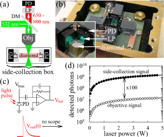
We constructed a prototype device to compare the side-collection technique to the conventional microscope objective method [Figs. 2(a)-2(c)]. This prototype instrument employed a [100]-oriented diamond chip ( ) grown via chemical vapor deposition (CVD) with a high NV-density (Apollo Diamond, Inc.) [Fig. 1(d)]. Four rectangular 650 nm longpass optical filters were placed in contact with the edges of the diamond. The filters transmitted most of the NV fluorescence band (), while reflecting scattered 532 nm excitation light. Four chip-style Si photodiodes were affixed to the backs of the filters. Because the filters were on a 2 mm thick quartz substrate, large active-area photodiodes (6 mm x 7 mm) were employed to maximize the detection acceptance angle. Future designs may be simplified using reflective coatings on several diamond surfaces and integrated filters on the photodiodes.
We calibrated the prototype device’s photon side-collection efficiency by comparing it against a microscope objective with known . Light from a 532 nm laser was focused into the diamond sample by a microscope air-objective (NA=0.40) [Fig. 2(a)]. The objective also collected NV fluorescence, and directed it to a filter and photodiode identical to those used for side-collection. The objective’s low NA guaranteed that its line-of-sight was not obstructed by the side-collection filters. In Fig. 2(d) we compare the integrated number of photons detected with the two collection modalities during a laser pulse, at various laser powers. The integrated photon count was measured by alternately connecting a charge-sensitive amplifier (Cremat Inc. CR-112) to the photodiode(s) of the two collection paths, and recording the average signal amplitude [Fig. 2(c)]. We found that the side-collection signal had a times larger photon count than the microscope objective signal under identical experimental conditions. The theoretically-estimated collection efficiency for the microscope objective was 0.59%.Sup Transmission losses through the objective, dichroic, and filter reduced the fraction of light reaching the detector to . The average quantum efficiency of the photodiode within the NV emission band at near-normal incidence , indicating . This implies that the NV fluorescence detection efficiency of the side-collection prototype device , while the fraction of photons reaching the four side-collection photodiodes (over a wide range of incidence angles) was . We also confirmed that the optical signals in the two detection paths were due to NV fluorescence by sweeping the frequency of a microwave field across the characteristic NV electron spin resonance at 2.87 GHz.Gruber et al. (1997) Both detection paths had a typical and nearly identical signal response, indicating that the side-collection filters selected NV fluorescence as effectively as conventional fluorescence microscopy.
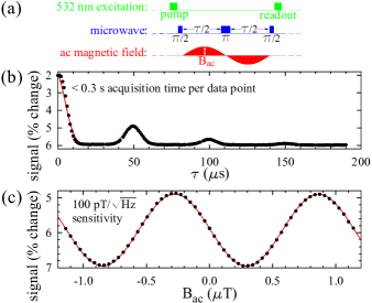
One important application of the side-collection technique is sensitive magnetometry using ensembles of NV spins in a diamond chip.Taylor et al. (2008); Pham et al. (2011) To demonstrate this application using the side-collection prototype device, we performed AC magnetometry with NVs contributing to the magnetometry signal in a laser excitation volume, using the standard spin-echo technique described in Ref. Maze et al., 2008 [Fig. 3(a)]. We applied a 37.5 G static magnetic field in the [111] direction, so that we could use an applied microwave field to resonantly select spin transitions of [111]-oriented NVs, as in Ref. Pham et al., 2011. (1/4 of the total number of NV spins are resonantly manipulated with this method, as NV orientations are distributed equally among the four crystallographic axes.) By sweeping the spin-echo duration (), we generated a coherence curve with revivals at even multiples of the nuclear precession period Maze et al. (2008) [Fig. 3(a)]. We extracted for this high NV-density diamond sample. We then generated the magnetometry curve in [Fig. 3(b)] by varying the amplitude of a 20 kHz AC magnetic field, with . From the slope of the curve and the standard deviation in the measurements at zero AC field amplitude, we found a magnetic field sensitivity , which to our knowledge is the best magnetic field sensitivity demonstrated to date with any NV-diamond system.Balasubramanian et al. (2009); Acosta et al. (2010) Note that this magnetic field sensitivity was limited by electrical noise in the detection circuitry of the prototype side-collection device, as verified by independent measurements. We expect that this added noise can be significantly reduced in future, optimized side-collection instruments, enabling greatly improved magnetic field sensitivity. For example, if the side-collection measurements for the current NV-diamond chip were instead limited by photon shot noise ( photons detected per measurement), then the magnetic field sensitivity would be . Sensitivities below could be achieved by using low-noise detection circuitry, increasing the measurement volume, and lengthening the NV through diamond engineering Balasubramanian et al. (2009) or dynamic decoupling techniques.Naydenov et al. (2011)
The photon detection enhancement of the side-collection technique has many other potential applications. For example, magnetometry may be extended to magnetic field imaging by using a thin layer of NVs near the diamond chip surface Pham et al. (2011) and scanning the laser focus while making time-resolved side-collection fluorescence measurements. The high signal-to-noise ratio provided by side-collection also greatly increases the speed of NV ensemble measurements, which may be used to study decoherence processes and develop NV spin manipulation protocols for magnetometry and quantum information. For example, the NV decoherence and magnetometry data shown in Fig. 3 was generated with of signal averaging time per data point, which is orders of magnitude shorter than the time that would be required to achieve comparable signal-to-noise using a microscope objective. The side-collection technique should also be applicable to single NV measurements using a tightly-focused laser beam for NV excitation. However, because side-collection accepts out-of-focus light, an ultra-pure diamond would likely be required to isolate single NVs in the excitation volume. This condition becomes less restrictive if a stimulated emission depletion (STED) microscope is employed,Rittweger et al. (2009) and we note that side-collection could increase the speed and precision of such super-resolution techniques, including combined NV super-resolution imaging and magnetometry (mag-STED).Maurer et al. (2010) Furthermore, the higher photon count rate provided by side-collection would improve NV quantum-state readout fidelity, and may be used in conjunction with existing techniques to achieve single-shot readout of the NV spin for quantum information applications.Jiang et al. (2009)
We gratefully acknowledge the provision of diamond samples by Apollo Diamond and Element Six; and also informative discussions with Patrick Doering, David Glenn, and Alexei Trifonov. This work was supported by NIST, NSF, and DARPA (QuEST and QuASAR programs).
References
- Aharonovich et al. (2011) I. Aharonovich, S. Castelletto, D. A. Simpson, C.-H. Su, A. D. Greentree, and S. Prawer, Rep. Prog. Phys. 74, 076501 (2011).
- Jelezko et al. (2004) F. Jelezko, T. Gaebel, I. Popa, A. Gruber, and J. Wrachtrup, Phys. Rev. Lett. 92, 076401 (2004).
- Balasubramanian et al. (2009) G. Balasubramanian, P. Neumann, D. Twitchen, M. Markham, R. Kolesov, N. Mizuochi, J. Isoya, J. Achard, J. Beck, J. Tissler, V. Jacques, P. R. Hemmer, F. Jelezko, and J. Wrachtrup, Nat. Mater. 8, 383 (2009).
- Beveratos et al. (2001) A. Beveratos, R. Brouri, T. Gacoin, J.-P. Poizat, and P. Grangier, Phys. Rev. A 64, 061802 (2001).
- Babinec et al. (2010) T. M. Babinec, B. J. M. Hausmann, M. Khan, Y. Zhang, J. R. Maze, P. R. Hemmer, and M. Loncar, Nat. Nanotechnol. 5, 195 (2010).
- Dutt et al. (2007) M. V. G. Dutt, L. Childress, L. Jiang, E. Togan, J. Maze, F. Jelezko, A. S. Zibrov, P. R. Hemmer, and M. D. Lukin, Science 316, 1312 (2007).
- Jiang et al. (2009) L. Jiang, J. S. Hodges, J. R. Maze, P. Maurer, J. M. Taylor, D. G. Cory, P. R. Hemmer, R. L. Walsworth, A. Yacoby, A. S. Zibrov, and M. D. Lukin, Science 326, 267 (2009).
- Togan et al. (2010) E. Togan, Y. Chu, A. S. Trifonov, L. Jiang, J. Maze, L. Childress, M. V. G. Dutt, A. S. Sorensen, P. R. Hemmer, A. S. Zibrov, and M. D. Lukin, Nature 466, 730 (2010).
- Rittweger et al. (2009) E. Rittweger, K. Y. Han, S. E. Irvine, C. Eggeling, and S. W. Hell, Nat. Photonics 3, 144 (2009).
- Maurer et al. (2010) P. C. Maurer, J. R. Maze, P. L. Stanwix, L. Jiang, A. V. Gorshkov, A. A. Zibrov, B. Harke, J. S. Hodges, A. S. Zibrov, A. Yacoby, D. Twitchen, S. W. Hell, R. L. Walsworth, and M. D. Lukin, Nat. Phys. 6, 912 (2010).
- Maze et al. (2008) J. R. Maze, P. L. Stanwix, J. S. Hodges, S. Hong, J. M. Taylor, P. Cappellaro, L. Jiang, M. V. G. Dutt, E. Togan, A. S. Zibrov, A. Yacoby, R. L. Walsworth, and M. D. Lukin, Nature 455, 644 (2008).
- Balasubramanian et al. (2008) G. Balasubramanian, I. Y. Chan, R. Kolesov, M. Al-Hmoud, J. Tisler, C. Shin, C. Kim, A. Wojcik, P. R. Hemmer, A. Krueger, T. Hanke, A. Leitenstorfer, R. Bratschitsch, F. Jelezko, and J. Wrachtrup, Nature 455, 648 (2008).
- Pham et al. (2011) L. M. Pham, D. Le Sage, P. L. Stanwix, T. K. Yeung, D. Glenn, A. Trifonov, P. Cappellaro, P. R. Hemmer, M. D. Lukin, H. Park, A. Yacoby, and R. L. Walsworth, New J. Phys. 13, 045021 (2011).
- (14) See supplementary material for derivations of microscope objective collection efficiencies and the estimated side-collection efficiency.
- Tisler et al. (2009) J. Tisler, G. Balasubramanian, B. Naydenov, R. Kolesov, B. Grotz, R. Reuter, J.-P. Boudou, P. A. Curmi, M. Sennour, A. Thorel, M. Börsch, K. Aulenbacher, R. Erdmann, P. R. Hemmer, F. Jelezko, and J. Wrachtrup, ACS Nano 3, 1959 (2009).
- Stanwix et al. (2010) P. L. Stanwix, L. M. Pham, J. R. Maze, D. Le Sage, T. K. Yeung, P. Cappellaro, P. R. Hemmer, A. Yacoby, M. D. Lukin, and R. L. Walsworth, Phys. Rev. B 82, 201201 (2010).
- Siyushev et al. (2010) P. Siyushev, F. Kaiser, V. Jacques, I. Gerhardt, S. Bischof, H. Fedder, J. Dodson, M. Markham, D. Twitchen, F. Jelezko, and J. Wrachtrup, Appl. Phys. Lett. 97, 241902 (2010).
- Hadden et al. (2010) J. P. Hadden, J. P. Harrison, A. C. Stanley-Clarke, L. Marseglia, Y.-L. D. Ho, B. R. Patton, J. L. O’Brien, and J. G. Rarity, Appl. Phys. Lett. 97, 241901 (2010).
- Gruber et al. (1997) A. Gruber, A. Dräbenstedt, C. Tietz, L. Fleury, J. Wrachtrup, and C. v. Borczyskowski, Science 276, 2012 (1997).
- Taylor et al. (2008) J. Taylor, P. Cappellaro, L. Childress, L. Jiang, D. Budker, P. R. Hemmer, A. Yacoby, R. Walsworth, and M. D. Lukin, Nat. Phys. 4, 810 (2008).
- Acosta et al. (2010) V. M. Acosta, E. Bauch, A. Jarmola, L. J. Zipp, M. P. Ledbetter, and D. Budker, Appl. Phys. Lett. 97, 174104 (2010).
- Naydenov et al. (2011) B. Naydenov, F. Dolde, L. T. Hall, C. Shin, H. Fedder, L. C. L. Hollenberg, F. Jelezko, and J. Wrachtrup, Phys. Rev. B 83, 081201 (2011).