Imaging topologically protected transport with quantum degenerate gases
Abstract
Ultracold and quantum degenerate gases held near conductive surfaces can serve as sensitive, high resolution, and wide-area probes of electronic current flow. Previous work has imaged transport around grain boundaries in a gold wire by using ultracold and Bose-Einstein condensed atoms held microns from the surface with an atom chip trap. We show that atom chip microscopy may be applied to useful purpose in the context of materials exhibiting topologically protected surface transport. Current flow through lithographically tailored surface defects in topological insulators (TI)—both idealized and with the band-structure and conductivity typical of Bi2Se3—is numerically calculated. We propose that imaging current flow patterns enables the differentiation of an ideal TI from one with a finite bulk–to–surface conductivity ratio, and specifically, that the determination of this ratio may be possible by imaging transport around trenches etched into the TI’s surface.
pacs:
03.75.Be,73.25.+i,67.85.HjI Introduction
The topological insulator is a unique state of topologically non-trivial quantum matter that has sparked a tremendous amount of interest in the condensed matter community Hasan and Kane (2010); Qi and Zhang (2011). Interest is not only focused on the novel manner in which this matter organizes, which is distinct from the standard Landau symmetry-breaking paradigm, but also on the potential use of topological insulators in spintronic devices and in topologically protected quantum information processing Fu et al. (2007); Moore and Balents (2007); Qi et al. (2008); Schnyder et al. (2008); Leijnse and Flensberg (2011). The former application may arise from the strong spin-momentum locking of electron transport in the surface state. In heterostructures formed with, i.e., superconductors or topological superconductors, novel electronic excitations, particularly Majorana fermions, may arise whose manipulation (braiding) is thought to provide a means with which to engineer topologically protected quantum computation Hasan and Kane (2010); Qi and Zhang (2011).
Unfortunately, all known topological insulator materials suffer from large bulk conduction: they are not truly insulating due to chemical imperfections Qi and Zhang (2011) and so are not readily amenable to traditional transport measurements. For example, in the ternary chalcogenide Bi2Te2Se, the surface–to–bulk conductivity ratio is 6% Ren et al. (2010), though the measurements on the exact ratio differ Xiong et al. (2012). This makes surface transport properties very difficult to measure, let alone manipulate Analytis et al. (2010a); Steinberg et al. (2011). A challenge lies in acquiring the ability to distinguish, via transport, the interesting surface state dynamics from the less interesting dynamics in the bulk. Only then will the promise of novel electronic devices, exotic quantum phenomena, and quantum information processors be realized with topological insulators.
While the existence of the topologically protected surface state has been unambiguously detected in angle-resolved photoemission spectroscopy (ARPES) Chen et al. (2009); Hsieh et al. (2009) and scanning tunneling microcopy (STM) Roushan et al. (2009); Alpichshev et al. (2011); Beidenkopf et al. (2011) experiments, none of these techniques directly probe surface transport, which the aforementioned applications rely upon for functionality. But more fundamentally, there is significant disagreement Analytis ; Butch et al. (2010) about the nature of the surface state itself due to contradictory measurements from the disparate techniques of APRES, STM, quantum oscillations, and Hall conductance measurements Taskin and Ando (2009); Analytis et al. (2010a); Ren et al. (2010); Qu et al. (2010); Checkelsky et al. (2011); Butch et al. (2010). Band structure may bend at surfaces, inducing a crossing of the Fermi energy only at the surface, and surface probes, such as ARPES and STM, may then give a skewed picture of the material as a whole Analytis et al. (2010b); Butch et al. (2010). Conduction band states in the doped bulk form a parallel conducting path that cannot be effectively removed by electrostatic gating Steinberg et al. (2010) and traditional transport and Hall measurements on samples of varying geometry require a number of assumptions to analyze transport data, even on nanosamples Steinberg et al. (2011); Analytis . Time-resolved fundamental and second harmonic optical pump-probe spectroscopy can reveal differences in transient responses in the surface versus bulk states Hsieh et al. (2011), but this detection method does not isolate transport properties in the surface from the bulk.
Extant methods are not wholly satisfying from the standpoint of robustly detecting topologically protected surface states in presumptive topological insulators in a relatively model-independent fashion. By contrast, this proposal presents an independent technique that enables the direct detection of the surface current in a manner that provides a relatively model-free measure of the surface conductivity versus the bulk conductivity. This information may prove crucial in attempts to improve material growth techniques for obtaining more ideal topological insulators, such as those amenable to the spintronic and topologically protected quantum information processing applications mentioned above.
The atom chip microscope presented here may also advance topological insulator physics in other manners. The surface state of existing topological insulators seems to be fragile in that over time and exposure, APRES and terahertz spectroscopy have shown modifications to the surface and bulk states Kong et al. (2011); Valdés Aguilar et al. . Such aging effects will hamper device functionality unless fabrication techniques mitigate this effect. A surface transport probe such as we propose should be a powerful tool to diagnose these aging effects under various preparation conditions. Moreover, dynamically adding magnetic impurities to the surface breaks time-reversal symmetry in a way that should disrupt surface transport of the Dirac state Wray et al. (2011); Analytis . The cryogenic atom chip microcope would be well-poised to observe such dynamics.
Taking a long-term perspective, the proposed microscope serves a dual purpose in that it may enable the coherent coupling of matter waves to Majorana fermions, for either imaging or for building topologically protected quantum hybrid circuits Leijnse and Flensberg (2011). Indeed, the atom chip microscope may serve as an interesting probe of transport in topological superconducting systems of copper intercalated Bi2Se3 Hor et al. (2010); Sasaki et al. (2011).
In this work, we examine the possibility of utilizing magnetic field signatures from electronic transport in TIs as a means of characterizing the topologically protected surface state. Specifically, we propose the use of atom chips—substrates supporting micron-sized current-carrying wires that create magnetic microtraps near surfaces for thermal gases or Bose-Einstein condensates (BECs)—to enable single-shot and raster-scanned large-field-of-view detection of magnetic fields emanating from electronic transport in a TI. A previous proposal noted the utility of atom chip microscopy in the context of imaging transport in two-dimensional electron gases and employing these electron gases for atom trapping Sinuco-León et al. (2011).
Figures 2 and 3 depict the principles of atom chip trapping and the atom chip microscope, respectively. (The figure captions contain the descriptions of the geometry and measurement scheme.) Cryogenic atom chip microscopy introduces very important features to the toolbox of high-resolution, strongly correlated and topological material microscopy: simultaneous detection of magnetic and electric fields (down to the sub-single electron charge level); no invasive large magnetic fields or gradients; simultaneous micro- and macroscopic spatial resolution; freedom from 1/ flicker noise at low frequencies; and the complete decoupling of probe and sample temperatures. This latter feature is important since cooling topological insulator samples below 100 K is typically necessary to maximize sample resistivity.
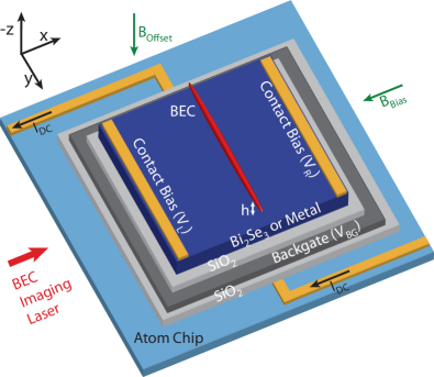
We begin by describing atom chip microscopy Wildermuth et al. (2005, 2006); Aigner et al. (2008) and conclude with a scheme to measure the surface-to-bulk conductance ratio from the resulting DC magnetic field using this technique. In support of this scheme, we calculate spatially resolved currents to understand the effect of doping on surface transport in Bi2Se3 thin films. Bi2Se3 is of particular interest because its bulk gap can be as high as 0.3 eV, though recent experiments have shown that the Fermi level in the bulk is usually pinned to the conduction band (CB) by Se vacancies, requiring either gating or doping to suppress bulk states Checkelsky et al. (2011). We focus our attention on the transport dynamics of the system depicted in Fig. 1. Contacts located on the top left and right edges of the system induce a longitudinal current across the thin film channel while the back gate tunes the chemical potential. We compare current profiles in undoped and doped Bi2Se3 thin films and to that of a conventional metal conductor. We show that a corrugated surface on a topological insulator, in which columns of material are removed, e.g., with a focused ion beam (FIB), to form trenches on the top surface, provides a unique environment to magnify the contrast between surface and bulk current and allows one to extract the surface-to-bulk conductance ratio from single-shot or multishot atom chip microscopy measurements.
II Imaging transport via atom chip microscopy
We now describe the atom chip trapping technique Reichel et al. (2001); Folman et al. (2002); Fortagh and Zimmermann (2007). The proposed transport probe of TIs consists of a collection of trapped ultracold or Bose-condensed neutral atoms. While simple quadrupole magnetic traps formed from anti-Helmholtz coils—and variations thereof which produce harmonic traps—are sufficient for exploring many aspects of ultracold atomic physics, such macroscopic coils are poorly suited for accurately bringing gases within microns of a surface.
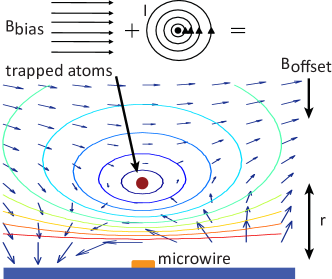
Shrinking coils to the micron scale can greatly enhance the trap’s gradient and curvature. A microtrap’s gradient and curvature scale as and , respectively, where is the wire current and is the trap center-to-wire distance. Currents of 100 mA and wire cross sections of a few square microns are required to obtain high trap gradients () and curvatures () at small . Unfortunately, mounting such coils in a UHV chamber suitable for laser cooling is not practical. Fortunately, fields with similar trap gradient and curvature scaling laws may be obtained from microfabricated wires on a planar substrate. When combined with a weak, easily produced homogenous bias field , such microwires create extremely tight magnetic traps for atoms suspended above the surface Weinstein and Libbrecht (1995). Full accessibility for nearby solid-state materials is preserved. The robust loading, confinement, and detection of ultracold atoms using chip-based traps has been demonstrated down to m Lin et al. (2004); Krüger ; Krüger et al. (2005); Smith et al. (2011), including atom chip trap-based BEC production (see Ref. Fortagh and Zimmermann (2007) for review). Condensate lifetimes above dielectrics have been measured to be greater than 1 s with minimal atom loss at distance Lin et al. (2004). The same trap stability is expected over the thin metals employed here, where the metal thickness is less than the skin depth and Henkel et al. (1999); Henkel and Pötting (2001): Surface state thickness in ideal TIs should be less than the 150-nm thickness of the metallic mirror coated on top of the sample (over a thin insulating intermediate layer), and non-ideal, doped TIs naturally have larger bulk resistivities (1 cm) than, e.g., gold Ren et al. (2010). We will not discuss here the well-established atom chip trapping procedures, imaging techniques, or considerations of surface Casimir-Polder potentials, but rather refer the reader to the extant literature Reichel et al. (2001); Folman et al. (2002); Lin et al. (2004); Fortagh and Zimmermann (2007); Sinuco-León et al. (2011).
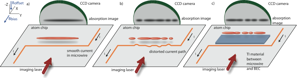
While BEC production using atom chips is now a mature technology, a major spoiler of device functionality has been the disturbance of the otherwise smooth trap potential from the very current-carrying conductors that form it. The meandering current in wires due to scattering centers—and thus magnetic field inhomogeneities at the ppm level—cause fragmentation of the trapped BEC into “sausage-link” like mini-BECs Fortagh and Zimmermann (2007). This fragmentation inhibits matter wave transport once the BEC chemical potential is less than local potential maxima.
However, this surprisingly sensitive susceptibility of atom traps to magnetic field perturbations is a feature we propose to exploit for the study of transport in TIs. By a simple rearrangement of the trapping bias field and microwire current path, atoms can be placed far away from the trapping wire ( m) but within microns above a material whose magnetic and electric field inhomogeneities are of interest. Figure 3 depicts the operating principle of the atom chip microscope in which the density of a BEC is perturbed by a TI sample without adverse affects from the trapping wire itself. A recent experiment demonstrated the use of a Rb-based atom chip to image current flow in a room temperature gold wire with 10-m resolution (3-m magnetic field resolution) and sub-nT sensitivity Wildermuth et al. (2005, 2006). Imaging at m provided 3-m-resolution of sub-mrad deviations in current flow angle Aigner et al. (2008). With improvements to imaging systems, e.g., using high-numerical and aberration-corrected lens systems Zimmermann et al. (2011), resolution of transport flow at the 1 to 2-m-level should be possible.
The atom chip microscopy measurements in this proposal requires the easily obtained confinement of a cigar-shaped BEC within – m Lin et al. (2004) from a TI surface. The axis of the BEC lies along and can be positioned anywhere along for imaging the magnetic field from the transport flow between the two bias contacts. With easily achievable microwire currents and bias magnetic fields , the harmonic trapping potential may possess transverse frequencies approaching 1 kHz while maintaining the axial frequency below 10 Hz. A field of 1 G at the trap minimum is achievable, which serves to prevent loss and heating from Majorana spin flips. Small inhomogeneous fields transverse to the cigar-shaped BEC do not affect the density of the BEC due to the high transverse trapping frequencies. However, inhomogeneous fields along the BEC axis, even at the nT level, can easily perturb the BEC density due to its low chemical potential and weakly confining trap frequency. Thus, the cigar-shaped, quasi-1D BEC serves as a vector-resolved magnetic field sensor, measuring field modulations along the condensate axis , where is the atomic magnetic moment, is the s-wave scattering length of the atoms, and is the BEC’s 1D density Aigner et al. (2008). The source current is derived from the local magnetic field map via application of the Biot-Savart law Wildermuth et al. (2005, 2006); Aigner et al. (2008). Thus, the BEC serves to image transport as well as the local magnetic field inhomogeneties: The sensed fields along primarily arise from transport transverse to the BEC axis—i.e., in the -plane—allowing the BEC to detect deviations in both the depth and angle of transport. Though for the measurements of surface–to–bulk conductivity ratio presented below in Sections IV and V, the condensate is primarily sensitive to modulation in rather than angular deviation in . This is due to the very broad sample (and trenches) in , resulting in a -field arising from a sheet, rather than line, current at different depths in in the regions of imaging interest.
Ultracold, but thermal, gases may be used as well for better dynamic field range, though at the price of lower field sensitivity compared to a BEC: Aigner et al. (2008). The atomic gas density may be imaged above a surface assuming the top surface is made reflective with a 150 nm-thin metal film on thin insulator. With high-resolution BEC imaging optics, the distance of the gas from the TI surface sets the transport imaging resolution of the atom chip microscope. The Casimir-Polder potential and electrostatic patch field effects can distort magnetic traps and limit their lifetime within 1-m from a surface Lin et al. (2004); McGuirk et al. (2004); Obrecht et al. (2007a, b). However, ultracold gases have been confined and imaged in atom chip traps at m and patch potentials have not been observed to affect such traps above at least 5 m Krüger ; Krüger et al. (2005); Smith et al. (2011). Since the magnitude of measured fields scale with potential driving the current, all constant perturbations due to Casimir-Polder and patch fields can be calibrated out of the transport imaging measurement. Moreover, measurements of the surface–to–bulk conductivity ratio, discussed in Sections IV and V, do not require resolution better than, e.g., 5 m, because the feature sizes of the trenched TI can be on the tens of micron length scale. Thus, only m surface heights are needed, and at these heights, Casimir-Polder and patch field effects will not significantly affect the trapping potential for atom chip microscopy even when imaging above trenched regions.
III Quantum transport calculation
We perform quantum transport calculations on doped and undoped Bi2Se3 thin films using the non-equilibrium Green’s function (NEGF) formalism Datta (2000). These calculations allow us to examine current flow in topological insulators along smooth and corrugated surfaces and compare these transport profiles with that of a single orbital metal.
For the TI, the 4-orbital effective Dirac Hamiltonian of Bi2Se3 is Zhang et al. (2009):
| (1) | ||||
where = C + D1k + D2(k+k) and = M - B1k - B2(k + k). The system is in the basis ; , where . By fitting the band structure to ab initio calculations Liu et al. (2010), the material parameters of Bi2Se3 that we use in this work are M = 0.28 eV, A1 = 2.2 eV , A2 = 4.1 eV , B1 = 10.0 eV , B2 = 56.6 eV , C = -0.0068 eV, D1 = 1.3 eV , and D2 = 19.6 eV . We discretize into a nearest-neighbor real-space cubic lattice basis suitable for low energy transport (with a lattice constant , see Appendix A), and we evaluate spatially resolved current from point to with
| (2) | ||||
are the electron and hole correlation functions calculated within NEGF Datta (2005) and represents the off-diagonal block connecting sites and , which is only nonzero for nearest neighbors.
We define the Hamiltonian for a metal channel used for comparison with the TI systems with an isotropic single-orbital tight binding Hamiltonian,
| (3) |
where the hopping energy is set to eV, creates a fermion at site and denotes nearest-neighbor bonds in all three spatial directions. The corresponding DC magnetic field from transport in either the TI or the metal is calculated from the current profile using the Biot-Savart law 111The magnetic susceptibility of Bi2Se3 is less than 10-6 cm3 mol-1 Uemura and Satow (1977)..
III.1 Transport profiles
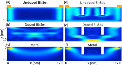
We first describe numerical results comparing the spatially resolved current profiles for thin films of undoped Bi2Se3, doped Bi2Se3, and metallic thin films in Fig. 4. The dimensions of the system are limited by computational time to a channel 17.6 nm (44 sites) in by 10.0 nm (25 sites) in and with periodic boundary conditions in the transverse direction, which is translationally invariant in our geometries. The contacts are placed only on the top surface () at and 17.6 nm and stretch along the entire -direction. The contact biases are set to VL= -VR = 0.09 V so that injected carriers are confined within the bulk gap of eV and thus pass only through surface states if the system is undoped. Current flows along the topologically nontrivial surface states of the undoped Bi2Se3 [see Fig. 4(a)], decaying into the bulk with a length scale of 3 nm along the top and bottom surfaces and 5 nm along the side surfaces. The discrepancy is due to the anisotropy in the effective velocity in the and directions, a consequence of the anisotropic quintuple layer structure of Bi2Se3. We note that the current profile of the undoped system qualitatively retains this shape for all biases within the bulk gap.
Transport in an undoped, ideal Bi2Se3 sample with a perfectly insulating bulk is carried only through surface states. Since most Bi2Se3 thin films are not ideal, however, there is a finite bulk conductivity, and it is desirable to devise a scheme which can show clear evidence of the topological surface states in the presence of bulk doping. We show in the following section that our proposed geometry provides a means to measure the degree of doping in the system.
Recent experiments Steinberg et al. (2010) on Bi2Se3 thin films point to an inhomogeneous distribution of doping in which the chemical potential is smoothly raised along the bottom half of the TI. However, we simply assume a homogenous doping profile of 0.2 eV above the Dirac point of the surface states. We have checked that our qualitative conclusions do not change if different doping profiles are used. Figure 4(b) shows the resulting current profile when the chemical potential is raised to 0.2 eV above the Dirac point. A parallel conducting path in the bulk limits topological flow along the top and bottom surface and there are significant increases in the total current.
For completeness, we study the transport behavior in a simple metallic thin film. Such transport starkly differs from ideal topologically nontrivial systems. Hopping in the metal is isotropic, and we see in Fig. 4(c) that current diffuses into the gapless bulk. (The current profile is normalized to have the same total current the same as in the undoped Bi2Se3 simulation.) The metal retains this current profile regardless of bias strength or hopping energy. As a check on the validity of these numerical results, we calculate that current in the metal flows around circular patches of (non-metallic) disorder at approximately angles (see Appendix B). This is in good agreement with analytical calculations and with the angular dependence of current in a gold wire as experimentally observed using atom chip microscopy Aigner et al. (2008).
III.2 Transport around corrugations
Doped and undoped Bi2Se3 channels are capable of effecting different transport characteristics than topologically trivial materials, such as a simple metal. However, as Fig. 4(b) shows, doping can mask TI-specific transport signatures. We next seek to devise a channel geometry whose magnetic field response will provide a distinct signature of topological current flow. We show in Figs. 4(d–f) that the current profiles in Figs. 4(a–c) change dramatically when two trenches 1-nm (2 sites) wide in and 5-nm (12 sites) deep are formed on the top surface. In the undoped TI, Fig. 4(d) shows that current flows around the trench and along the surface between the trenches. In this configuration, with a 7-nm separation between trenches, we find that over 92% of top surface current flows within 3-nm of the top surface between trenches, with only a small degradation due to bulk tunneling. We note that the conductivity does not change when trenches are added, as the contacts still have access to the topologically protected surface states.
If the bulk doping is sufficient to open a parallel conducting path, however, surface and bulk states will hybridize and allow carriers to move through the bulk instead of closely following the engineered geometric path, as shown in Fig. 4(e). We find that top surface current between the trenches drops monotonically and approximately linearly as doping strength in the bulk is increased from zero to 0.2 eV. (See Fig. 7 and Appendix C for the dependence of surface current on doping in the bulk.) Current is pushed even further into the bulk for the simple metal [Fig. 4(f)], with otherwise little qualitative change. As expected, there is a decrease in conductivity of the trenched metal which is proportional to the change in effective cross-sectional area.
IV Magnetic field from transport
Atom-chip microscopy does not measure the current directly, but rather the magnetic fields produced from the currents. The calculations depicted in Fig. 4 demonstrate a clear qualitative distinction between topologically non-trivial and trivial current flow in corrugated systems due to pinning of TI conducting state wavefunctions to the surface. Such surface states, in contrast to bulk states, generate clear signatures in the magnetic field produced by DC current flow. Corrugating the surface structure accentuates the surface current signature by inducing flow along paths with sharp discontinuities. The field from such flow is fundamentally different than that of a metal or heavily doped TI.
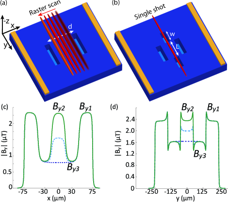
Three methods may be used to distinguish an ideal TI with no doping [Fig. 4(d)] from one with doping [Fig. 4(e)]. Method (a) involves raster-scan imaging the field modulation along an -oriented line centered symmetrically above the trenches. This field arises from the -modulation of the primarily -directed current [see Fig. 5(a)]. Method (b), similar to method (a), involves imaging the field modulation along a -oriented line centered symmetrically above the additional trenches depicted in Fig. 5(b). Method (c) involves imaging the field arising from current modulation around the corners of the trenches. At a distance from the surface, where is the trench separation in Fig. 5(a), the amplitude of the signal in method (c) is less than a factor of two different between a doped versus an undoped TI. While current flow around the trench is in principle measurable, we chose to focus this work on methods (a) and (b) because they provide a signal of much stronger contrast for distinguishing the degree of doping in a TI.
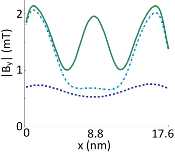
In method (a), the -component of the magnetic field above a line connecting the centers of the parallel trenches is measured in a multishot, raster-scan fashion. Figure 6(a) plots this magnetic field nm above the surface of each material system. The undoped TI system shows a peak in between the trenches due to surface current flow that approaches the maximum value halfway between the trenches. The peak signature in the doped TI is reduced due to the spatial separation of bulk current; a small decrease in between the trenches is attributed to the surface current remnant. The magnetic field response smoothly connects the undoped to the doped case as the surface-to-bulk conductance ratio increases. This effect provides a detection channel through which one may estimate the doping level from the surface-to-bulk conductance ratio, as discussed in more detail in Sec. V. Additionally, the field from TIs show a much sharper increase to either side of the trench pair when compared with the conventional metal model: The topological system, regardless of doping, produces a transport pattern distinct from simple metals because current does not immediately move into the bulk.
For an undoped TI, surface current magnitude does not appreciably change when trenches are added. Surface conductance dominates, and is nearly as large between the trenches as it is outside of the trenches; the small discrepancy arises from current flowing in around the trenches, which results in a reduction of roughly 5% in our model system. This effect would be less prominent in systems of larger size. Elastic backscattering in the highly doped system via bulk channels, however, causes a slight decrease in the average magnitude of .
Unfortunately, our simulations are confined to small dimensions due to the computational cost of the formalism. Matrix sizes of the 3D system quickly become intractable due to memory constraints even when translational invariance in the transverse direction is exploited. Thus, we are not able to numerically simulate systems that are of the necessary size for atom-chip microscopy. Fortunately, doping yields effects on transport regardless of trench size, channel dimensions, or aspect ratios, and the contrast in the field from surface versus bulk current is insensitive to system size. Over long length scales, inelastic scattering may harm the spin-orbit locking of the topologically protected surface state, but the existence of a conduction state at the surface remains regardless of system size. In other words, while this scattering will dephase the spins in the system, we do not anticipate a significant depreciation in surface current flow as the impurity scattering would be too weak to induce significant bulk current flow or backscattering. Therefore, the average magnitude of should remain nearly constant in large samples.
Current transport would generate a similar magnetic field if the system were expanded to be larger so that the channel and trench sizes in Fig. 6(a) were of m rather than nm scale. Figure 5(c) shows at 1 m from the surface when length scales are enlarged by to accommodate the atom chip microscope resolution. For the same surface current density, the resulting field is smaller, T, which is well above the nT sensitivity of atom chip microscopy. Currents smaller could be used to minimize resistive heating while still generating a detectable field signature. The field calculation is described in further detail in Appendix D. Similarly measurable profiles at lower fields may be measured at m, which are heights more optimal for avoiding complications due to Casimir-Polder effects. Adding more trenches to the TI surface in an array is expected to further accentuate the transport signals of interest.
Method (b), while requiring four, rather than two, trenches, is a single-shot technique for measuring an analogous transport profile to that shown in Fig 5(c). (Additional complexity in fabricating multiple trenches is not prohibitive.) Figure 5(b) shows how the ultracold atomic cloud—a length of 800 m was imaged in Ref. Krüger et al. (2007) in one shot—could extend over two lateral trenches in addition to the space between the pair of trenches oriented along the current flow. The resulting magnetic field detected by the microscope, shown in Fig. 5(d), is qualitatively similar to that recorded in method (a). Method (b) is much simpler and faster, however.
V Determination of surface–to–bulk conductance ratio
In order to determine the surface–to–bulk conductance ratio, we consider three points in the magnetic field plots of either Fig. 5(c) or (d): the maximum outside the trenches , the maximum directly between the trenches , and the minimum directly above one of the trenches . The ratio of surface current between the trenches to surface current in an ideal system obeys the phenomenological equation:
| (4) |
Equation 4 yields a ratio of 92% for the undoped system, compared to the actual value of 92% in the simulation. Current in and limited system sizes cause a deviation in that is ameliorated by larger trench sizes and larger separation between the trenches. Equation 4 provides a measure of given a microscopic model for , and the surface–to–bulk conductivity ratio may be determined by measuring the total current through the system. Fortunately, a microscopic model for is unnecessary if one calibrates the dependance of versus doping level, as we now explain.
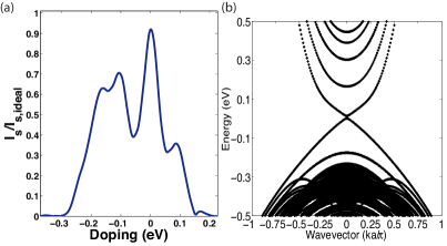
Consider the decay of surface current between the trenches as doping strength varies: Figure 7(a) shows how surface current between the trenches changes relative to the expected surface current in Bi2Se3. When the backgate tunes the effective doping to be directly at the Dirac point of Bi2Se3 (compensating any intrinsic doping), surface current reaches 92% of its ideal value when trenches are added. The relationship between surface current decay and doping strength is approximately linear until a bulk band is reached: the additional bulk states cause surface current to modulate. However, the overall effect near the Dirac point is monotonic and allows for the magnetic field response to smoothly map the transition from the undoped to the doped regimes.
The backgate in Fig. 1 allows one to tune the effective doping level regardless of intrinsic doping level. By measuring in the multiple (a) or single shot (b) method of Section IV, one obtains a full curve as in Fig. 7(a). The curve in Fig. 7(a) is less monotonic than it would be had the simulation been immune to finite-size effects. Experimental samples would be larger and exhibit fewer modulations. Nevertheless, such a curve will always have its global maximum at the point where the Fermi level reaches the Dirac point. This is also where , and combined with a two-probe transport measurement of at high gate bias, such a measurement provides a model-independent calibration of the curve. Mobility ratio in the bulk and surface can be determined by comparing the total current at this Dirac point backgate bias with a backgate bias far from this peak (e.g., near eV in Fig. 7). Thus, determination of the bulk–to–surface conduction ratio can be accomplished in a relatively model-independent fashion. (See Appendix C for discussion of the curve and band structure in the idealized TI case.)
VI Conclusion
Ultracold atom chip microscopy is capable of sensing a magnetic field signature of topological current flow. Similarly, vector field imaging with diamond NV centers Maze et al. (2008); Steinert et al. (2010) may be able to sense the field from transport. However, the higher spatial resolution of NV centers may be counterbalanced by their comparatively low DC field sensitivity (which is maximal at kHz frequencies), lower field dynamic range, and the longer scan time needed to paint a picture of the transport flow. (Though NV arrays with field detection alignment are under development.) By contrast, the mm-long ultracold atomic gas provides transport images in a single shot with micron-sized pixels.
We have shown that the contrast in magnetic field from transport in corrugated topological insulators provides a single-shot, relatively model-independent method for determining surface–to–bulk conductivity in Bi2Se3 thin films encumbered with Se vacancies. Realization of BECs coupled to fields from TIs or topological–superconductor heterostructures may open avenues for quantum hybrid circuits involving atomic ensemble quantum memory and qubit transduction.
Acknowledgements.
We would like to thank James Analytis, Ian Fisher, Lance Cooper, Peter Abbamonte, Richard Turner, and Matthew Naides for enlightening discussions. We acknowledge generous support from the U.S. Department of Energy, Office of Basic Energy Sciences, Division of Materials Sciences and Engineering under awards #DE-SC0001823 (B.L.L.) and #DE-FG02-07ER46453 (T.L.H.), and AFOSR award #FA9550-10-1-0459 (B.D. and M.J.G.).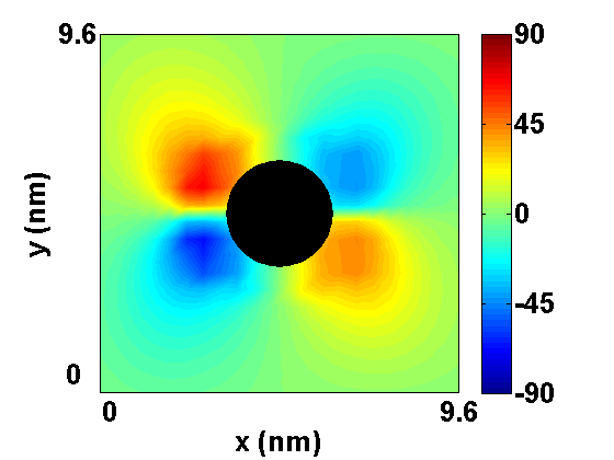
Appendix A Lattice Hamiltonian for Bi2Se3
The -space Dirac Hamiltonian for Bi2Se3 can be Fourier transformed into the real space Hamiltonian:
where () destroys (creates) a fermion at site (, , ), is the lattice constant and the matrices and material parameters are defined in Section III. Band structure calculations show the Dirac point occurs at 0.21 eV, with conduction band (CB) minimum and valence band (VB) maximum occurring at 0.31 eV and -0.02 eV, respectively. The back gate of the system tunes the Fermi energy to the Dirac point, where the real space Hamiltonian suitably describes low energy transport. When the effective lattice constant is set to 4 , nearest neighbor hopping energies are large enough for on-site energies within 0.3 eV of the Dirac point. The CB minimum is just over 0.1 eV above the Dirac point, and the bias configuration is accordingly set to VLVR = 0.09 V so that all injected carriers have energies within the bulk gap.
Appendix B Metallic transport around defects
The first use of atom chip microscopy demonstrated that current tends to move around impurities in a metal at 45∘ angles, as expected from analytical calculations Aigner et al. (2008). We replicate this observation as a cross-check of our numerics by placing a circular impurity 3 nm in diameter in the middle of the metal channel with bias configuration VL = -0.09 V and VR = 0.09 V. (Electron majority carriers flow from left to right.) Figure 8 shows that electrons primarily flow around the circular impurity at 45∘ angles before returning to a uniform current flow due to dissipation. The angular dependence is less prominent beyond the impurity, as dissipation is the cause of angular distortion in the metal rather than a sharp potential boundary as for the TIs. The single-orbital tight-binding Hamiltonian is thus a simple model that nevertheless produces a current profile retaining the salient physics of transport in disordered metals. As is the case in the trenched system, the angular dependence retains this characteristic shape of the current profile regardless of bias range or system size.
Appendix C Effect of doping on surface current in idealized TI
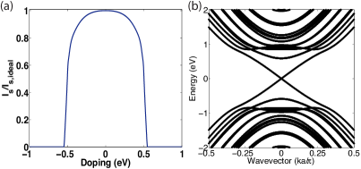
We perform an additional calculation with idealized TI parameters for the lattice Hamiltonian in Eq. A: M = 1.0 eV, A1 = A2 = 1.0 eV , B1 = B2 = 1.0 eV , C = 0.0 eV, D1 = D2 = 0.0 eV and Figure 9(a) explores the surface current ratio with this toy model using the same bias configuration as in the Bi2Se3 case (VL = -VR = 0.09 V). The gapless states are much more closely tied to the surface in this model, so tunneling between trenches is negligible when doping is zero, see Fig. 9. The ratio remains near unity until the CB minimum is reached, as the model has a much larger bulk gap. However, there is a decline in the ratio once the first CB minimum is reached at eV.
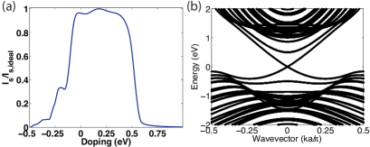
Particle-hole symmetry breaking biases the measurement of the backgate voltage at the point away from the Dirac point. Such asymmetry is induced by setting eV . Figure 10 shows simulations with particle-hole asymmetry demonstrating this effect. The peak is offset from the Dirac point, but by an amount given by the changed dispersion (Fermi velocity) at the Dirac point. Once measured, this effect may be accounted for in the calibration.
Appendix D Analytic calculation of magnetic field
The small systems sizes to which this formalism is limited prevents the trenches from completely isolating each component of the magnetic field response necessary for determining the surface–to–bulk conductance ratio. Undesirable contributions from current around the trenches cause a significant deviation of roughly 5% to the magnetic field response. To show how this is mitigated with larger system sizes—and to produce the plots in Fig. 6(c) and (d)—we compare results of the simulation to the analytical magnetic field response of a current carrying plate with equivalent geometry. Using the Biot-Savart law, the magnetic field response for a current-carrying wire going from point xl to xr in the longitudinal direction is
| (6) | |||||
| (7) | |||||
where and . We assume the points at which the magnetic field will be measured lie along the direction, directly above the middle of the channel, where y=0 and . The resulting magnetic field will have negligible and components due to the symmetry of a sheet current.
We now seek to take into account the width of the current carrying surface. According to Ampere’s law, the total magnetic field a distance above a horizontal current sheet of finite width and infinite length is
where W is the width of the channel. The magnetic field above a current plate thus decays proportionally to rather than a simple dependence. The change in the magnetic field magnitude caused by current moving in the bulk compared to current along the surface must be appreciable, thus the width should remain as small as possible so that the contrast remains high. For example, a width of 10 m is thin enough for the magnetic field to drop more than 50% when the trenches are 5 m deep and the atoms lie 1-2 m from the surface.
We define two functions for the magnetic field response due to and -directed current, which are respectively
These functions are used to calculate the magnetic field response of a current configuration analogous to those seen in Fig. 6 but for larger dimensions. We calculate the magnetic field response by summing over the entire width of the system.
The simulations yield a surface current density of 4.9 A nm-1, in good agreement with the analytic solution for current in Bi2Se3,
| (12) |
where kF is the Fermi wave vector, for an applied bias Vapp = VL - VR = 0.18 V. We ignore side surface current and assume the channel is deep enough that surface current contributions to the magnetic field around the bottom corners may be neglected. Homogeneous additions to the magnetic field will not change the calculation, as the surface–to–bulk ratio is determined by the magnetic field magnitude in between the trenches relative to the magnetic field above each trench. A similar calculation was used to create the field profile in Fig. 5(d).
References
- Hasan and Kane (2010) M. Z. Hasan and C. L. Kane, Rev. Mod. Phys. 82, 3045 (2010).
- Qi and Zhang (2011) X.-L. Qi and S.-C. Zhang, Rev. Mod. Phys. 83, 1057 (2011).
- Fu et al. (2007) L. Fu, C. L. Kane, and E. J. Mele, Phys. Rev. Lett. 98, 106803 (2007).
- Moore and Balents (2007) J. E. Moore and L. Balents, Phys. Rev. B 75, 121306 (2007).
- Qi et al. (2008) X.-L. Qi, T. L. Hughes, and S.-C. Zhang, Phys. Rev. B 78, 195424 (2008).
- Schnyder et al. (2008) A. P. Schnyder, S. Ryu, A. Furusaki, and A. W. W. Ludwig, Phys. Rev. B 78, 195125 (2008).
- Leijnse and Flensberg (2011) M. Leijnse and K. Flensberg, Phys. Rev. Lett. 107, 210502 (2011).
- Ren et al. (2010) Z. Ren, A. A. Taskin, S. Sasaki, K. Segawa, and Y. Ando, Phys. Rev. B 82, 241306 (2010).
- Xiong et al. (2012) J. Xiong, A. Petersen, D. Qu, Y. Hor, R. Cava, and N. Ong, Physica E 44 (2012).
- Analytis et al. (2010a) J. G. Analytis, R. D. McDonald, S. C. Riggs, J.-H. Chu, G. S. Boebinger, and I. R. Fisher, Nature Physics 6, 960 (2010a).
- Steinberg et al. (2011) H. Steinberg, J.-B. Laloë, V. Fatemi, J. S. Moodera, and P. Jarillo-Herrero, Phys. Rev. B 84, 233101 (2011).
- Chen et al. (2009) Y. L. Chen, J. G. Analytis, J.-H. Chu, Z. K. Liu, S.-K. Mo, X. L. Qi, H. J. Zhang, D. H. Lu, X. Dai, Z. Fang, S. C. Zhang, I. R. Fisher, Z. Hussain, and Z.-X. Shen, Science 325, 178 (2009).
- Hsieh et al. (2009) D. Hsieh, Y. Xia, D. Qian, L. Wray, J. H. Dil, F. Meier, J. Osterwalder, L. Patthey, J. G. Checkelsky, N. P. Ong, A. V. Fedorov, H. Lin, A. Bansil, D. Grauer, Y. S. Hor, R. J. Cava, and M. Z. Hasan, Nature 460, 1101 (2009).
- Roushan et al. (2009) P. Roushan, J. Seo, C. V. Parker, Y. S. Hor, D. Hsieh, D. Qian, A. Richardella, M. Z. Hasan, R. J. Cava, and A. Yazdani, Nature 460, 1106 (2009).
- Alpichshev et al. (2011) Z. Alpichshev, J. G. Analytis, J.-H. Chu, I. R. Fisher, and A. Kapitulnik, Phys. Rev. B 84, 041104 (2011).
- Beidenkopf et al. (2011) H. Beidenkopf, P. Roushan, J. Seo, L. Gorman, I. Drozdov, Y.-S. Hor, R. J. Cava, and A. Yazdani, Nature Physics 7, 939 (2011).
- (17) J. G. Analytis, (private communication, 2012) .
- Butch et al. (2010) N. P. Butch, K. Kirshenbaum, P. Syers, A. B. Sushkov, G. S. Jenkins, H. D. Drew, and J. Paglione, Phys. Rev. B 81, 241301 (2010).
- Taskin and Ando (2009) A. A. Taskin and Y. Ando, Phys. Rev. B 80, 085303 (2009).
- Qu et al. (2010) D.-X. Qu, Y. S. Hor, J. Xiong, R. J. Cava, and N. P. Ong, Science 329, 821 (2010).
- Checkelsky et al. (2011) J. G. Checkelsky, Y. S. Hor, R. J. Cava, and N. P. Ong, Phys. Rev. Lett. 106, 196801 (2011).
- Analytis et al. (2010b) J. G. Analytis, J.-H. Chu, Y. Chen, F. Corredor, R. D. McDonald, Z. X. Shen, and I. R. Fisher, Phys. Rev. B 81, 205407 (2010b).
- Steinberg et al. (2010) H. Steinberg, D. R. Gardner, Y. S. Lee, and P. Jarillo-Herrero, Nano Letters 10, 5032 (2010).
- Hsieh et al. (2011) D. Hsieh, F. Mahmood, J. W. McIver, D. R. Gardner, Y. S. Lee, and N. Gedik, Phys. Rev. Lett. 107, 077401 (2011).
- Kong et al. (2011) D. Kong, J. J. Cha, K. Lai, H. Peng, J. G. Analytis, S. Meister, Y. Chen, H.-J. Zhang, I. R. Fisher, Z.-X. Shen, and Y. Cui, ACS Nano 5, 4698 (2011).
- (26) R. Valdés Aguilar, L. Wu, A. V. Stier, L. S. Bilbro, M. Brahlek, N. Bansal, S. Oh, and N. P. Armitage, arXiv:1202.1249 .
- Wray et al. (2011) L. A. Wray, S.-Y. Xu, Y. Xia, D. Hsieh, A. V. Fedorov, Y. S. Hor, R. J. Cava, A. Bansil, H. Lin, and M. Z. Hasan, Nature Physics 7, 32 (2011).
- Hor et al. (2010) Y. S. Hor, A. J. Williams, J. G. Checkelsky, P. Roushan, J. Seo, Q. Xu, H. W. Zandbergen, A. Yazdani, N. P. Ong, and R. J. Cava, Phys. Rev. Lett. 104, 057001 (2010).
- Sasaki et al. (2011) S. Sasaki, M. Kriener, K. Segawa, K. Yada, Y. Tanaka, M. Sato, and Y. Ando, Phys. Rev. Lett. 107, 217001 (2011).
- Sinuco-León et al. (2011) G. Sinuco-León, B. Kaczmarek, P. Krüger, and T. M. Fromhold, Phys. Rev. A 83, 021401 (2011).
- Wildermuth et al. (2005) S. Wildermuth, S. Hofferberth, I. Lesanovsky, E. Haller, L. M. Andersson, S. Groth, I. Bar-Joseph, P. Krüger, and J. Schmiedmayer, Nature 435, 440 (2005).
- Wildermuth et al. (2006) S. Wildermuth, S. Hofferberth, I. Lesanovsky, S. Groth, P. Krüger, J. Schmiedmayer, and I. Bar-Joseph, Appl. Phys. Lett. 88, 264103 (2006).
- Aigner et al. (2008) S. Aigner, L. D. Pietra, Y. Japha, O. Entin-Wohlman, T. David, R. Salem, R. Folman, and J. Schmiedmayer, Science 319, 1226 (2008).
- Reichel et al. (2001) J. Reichel, W. Hänsel, P. Hommelhoff, and T. W. Hänsch, Appl. Phys. B 72, 81 (2001).
- Folman et al. (2002) R. Folman, P. Krüger, J. Schmiedmayer, J. Denschlag, and C. Henkel, Adv. At. Mol. Opt. Phys. 48, 263 (2002).
- Fortagh and Zimmermann (2007) J. Fortagh and J. C. Zimmermann, Rev. Mod. Phys. 79, 235 (2007).
- Krüger et al. (2007) P. Krüger, L. M. Andersson, S. Wildermuth, S. Hofferberth, E. Haller, S. Aigner, S. Groth, I. Bar-Joseph, and J. Schmiedmayer, Phys. Rev. A 76, 063621 (2007).
- Weinstein and Libbrecht (1995) J. D. Weinstein and K. G. Libbrecht, Phys. Rev. A 52, 4004 (1995).
- Lin et al. (2004) Y.-J. Lin, I. Teper, C. Chin, and V. Vuletić, Phys. Rev. Lett. 92, 050404 (2004).
- (40) P. Krüger, Ph.D. thesis, University of Heidelberg, (2004) .
- Krüger et al. (2005) P. Krüger, S. Wildermuth, S. Hofferberth, L. M. Andersson, S. Groth, I. Bar-Joseph, and J. Schmiedmayer, Journal of Physics: Conference Series 19 (2005).
- Smith et al. (2011) D. A. Smith, S. Aigner, S. Hofferberth, M. Gring, M. Andersson, S. Wildermuth, P. Krüger, S. Schneider, T. Schumm, and J. Schmiedmayer, Opt. Express 19, 8471 (2011).
- Henkel et al. (1999) C. Henkel, S. Pötting, and M. Wilkens, Appl. Phys. B 69, 379 (1999).
- Henkel and Pötting (2001) C. Henkel and S. Pötting, Appl. Phys. B 72, 73 (2001).
- Zimmermann et al. (2011) B. Zimmermann, T. Müller, J. Meineke, T. Esslinger, and H. Moritz, New Journal of Physics 13, 043007 (2011).
- McGuirk et al. (2004) J. M. McGuirk, D. M. Harber, J. M. Obrecht, and E. A. Cornell, Phys. Rev. A 69, 062905 (2004).
- Obrecht et al. (2007a) J. M. Obrecht, R. J. Wild, M. Antezza, L. P. Pitaevskii, S. Stringari, and E. A. Cornell, Phys. Rev. Lett. 98, 063201 (2007a).
- Obrecht et al. (2007b) J. M. Obrecht, R. J. Wild, and E. A. Cornell, Phys. Rev. A 75, 062903 (2007b).
- Datta (2000) S. Datta, Superlattices and Microstructures 28, 253 (2000).
- Zhang et al. (2009) H. Zhang, C.-X. Liu, X.-L. Qi, X. Dai, Z. Fang, and S.-C. Zhang, Nat Phys 5, 438 (2009).
- Liu et al. (2010) C.-X. Liu, X.-L. Qi, H. Zhang, X. Dai, Z. Fang, and S.-C. Zhang, Phys. Rev. B 82, 045122 (2010).
- Datta (2005) S. Datta, Quantum Transport: Atom to Transistor (Cambridge University Press, 2005).
- Note (1) The magnetic susceptibility of Bi2Se3 is less than 10-6 cm3 mol-1 Uemura and Satow (1977).
- Maze et al. (2008) J. R. Maze, P. L. Stanwix, J. S. Hodges, S. Hong, J. M. Taylor, P. Cappellaro, L. Jiang, M. V. G. Dutt, E. Togan, A. S. Zibrov, A. Yacoby, R. L. Walsworth, and M. . D. Lukin, Nature 455, 644 (2008).
- Steinert et al. (2010) S. Steinert, F. Dolde, P. Neumann, A. Aird, B. Naydenov, G. Balasubramanian, F. Jelezko, and J. Wrachtrup, Review of Scientific Instruments 81, 043705 (2010).
- Uemura and Satow (1977) O. Uemura and T. Satow, Physica Status Solidi (b) 84, 353 (1977).