Thermal properties of charge noise sources
Abstract
Measurements of the temperature and bias dependence of Single Electron Transistors (SETs) in a dilution refrigerator show that charge noise increases linearly with refrigerator temperature above a voltage-dependent threshold temperature, and that its low temperature saturation is due to SET self-heating. We show further that the two-level fluctuators responsible for charge noise are in strong thermal contact with the electrons in the SET, which can be at a much higher temperature than the substrate. We suggest that the noise is caused by electrons tunneling between the SET metal and nearby potential wells.
pacs:
73.50.Td, 85.35.Gv, 03.65.Yz, 65.80.-gI Introduction
Low-frequency charge noise with a power spectral density is observed in all charge sensitive devices ( is frequency and ). Apart from limiting the sensitivity of electrometers, such as the Single Electron Transistor (SET) Averin and Likharev (1991); Fulton and Dolan (1987), charge noise is a source of decoherence in qubits Paladino et al. (2002); Bylander et al. (2011) and gives rise to errors in metrological quantum standards Kautz et al. (2000); Covington et al. (2000); Bylander et al. (2005). The noise is usually attributed to a superposition of Lorentzian spectra, each generated by a Two-Level Fluctuator (TLF) consisting of a charged particle moving stochastically between two locationsMachlup (1954); Dutta and Horn (1981). In spite of extensive studies, both experimental and theoretical Dutta and Horn (1981); Zimmerli et al. (1992); Zorin et al. (1996); Zimmerman et al. (1997); Brown et al. (2006); Kafanov et al. (2008); Wolf et al. (1997); Song et al. (1995); Li et al. (2007); Henning et al. (1999); Krupenin et al. (2000); Kenyon et al. (2000); Astafiev et al. (2006); Starmark et al. (1999), the sources and locations of the TLFs remain unknown.
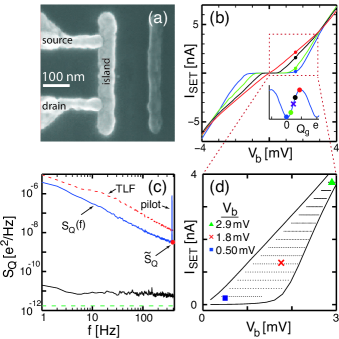
Because of its simplicity and unmatched charge sensitivity, the SET is an ideal tool to study the fundamentals of charge transport and noiseXue et al. (2009); Ubbelohde et al. (2012); Bylander et al. (2005), and its structural similarity to superconducting qubits and metrological devices means that knowledge gained from the SET can be carried over to these and other devices. The SET consists of a small metallic island connected via tunnel junctions to source and drain electrodes [Fig. 1(a)]. Its current-voltage (-) characteristic [Fig. 1(b)] depends strongly on the charge induced on the island by externally applied electric fields or charges moving in its surroundings, and this response is periodic in the electron charge [Fig. 1(b), inset].
The electrons moving through the SET deposit energy on the island in proportion to the bias voltage . To a good approximation, the power dissipated on the SET island is , and in a metallic SET this power is generally assumed to be dissipated rapidly into the electron gas. At low temperatures, the thermal coupling between the SET electrons and the phonons of the substrate is weak, and the temperature of the electron gas can be elevated significantly above that of the phononsKautz et al. (1993). The effect of this on the charge noise is discussed further below.
Several authors have found that the charge noise measured in SETs decreases as the temperature is lowered, saturating to a constant level at low temperature Song et al. (1995); Li et al. (2007); Henning et al. (1999); Krupenin et al. (2000); Kenyon et al. (2000); Astafiev et al. (2006). This saturation has been attributed to self-heating of the SET but, since there is no obvious model for thermalization between the TLFs and the SET electron gas, the issue remains open.
The influence of SET bias parameters on charge noise has also been studied Wolf et al. (1997); Henning et al. (1999); Krupenin et al. (2000), and while it is clear that the charge noise increases with SET bias, no quantitative conclusions have been drawn. This is largely due to the small range of useful bias voltages in SETs with modest charging energy, and the tendency of noise data to suffer from scattering and drift.
Here, we present three experiments on charge noise in SETs. Using SETs with relatively high charging energy and recording an extensive amount of data, we can clearly resolve the dependence of the noise on both refrigerator temperature, , and SET bias parameters. Our results demonstrate that the TLFs predominantly thermalize with the electron gas of the SET, rather than by a roundabout route through the substrate phonons. At high , the SET electrons (and hence the TLFs) are thermalized with the refrigerator temperature, so that the charge noise scales proportionally with . For low , self heating brings the SET electrons to a temperature , which causes the charge noise to saturate as is decreased. This is expected if the TLFs are occupied by electrons tunneling from the SET metal, but not for conventional double-well TLFs located entirely outside the SET. Thus, our data point to a scenario where the noise is dominated by single-well TLFs close to the SET junctions.
II TLF models
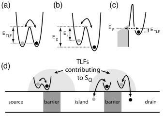
Regardless of their microscopic origins, TLFs can affect the SET only if they are located inside or in close vicinity to the tunnel junctions [Fig. 2(c)]. Based on the dependence of the charge noise on external electric fields, for a sample similar to ours, Zimmerman et al. were able to prove that the TLF ensemble must be at least partly located outside the tunnel barriersZimmerman et al. (1997).
The most common model for a charge TLF is that of a charged particle moving stochastically back and forth between two potential wells located in the dielectric material surrounding the device [Fig. 2(a)]. For each of the two wells, a different fraction of the TLF charge couples to the device, in the case of an SET as charge induced on its island. In the simplest model of a symmetric, two-well potentialDutta and Horn (1981), switching between states occurs with a characteristic time that is identical for the two directions. The resulting power spectrum is a Lorentzian of the form ; here . If, further, the process is thermally activated, , where is a characteristic attempt frequency and is the barrier height. Thus, for an ensemble of TLFs with a distribution of energies , the noise power spectrum becomes . The function is strongly peaked with a width of the order of . Finally, provided varies slowly on the scale of , Dutta and HornDutta and Horn (1981) show that , where is the energy at which peaks. This result demonstrates that for an ensemble of symmetric charge TLFs, .
Kenyon et al. Kenyon et al. (2000) extended this picture to an asymmetric double-well potential [Fig. 2(b)] in which each TLF has two different activation energies, one for each direction of switching. Under the assumptions that the two switching processes are independent and the two energies are uniformly distributed over the ensemble of TLFs, each process contributes a factor scaling as to the power spectrum, leading to .
It has also been proposed that each TLF consists of a single potential well, with electrons tunneling back and forth between the well and the conductors of the deviceBrown et al. (2006); Kafanov et al. (2008); Simkins et al. (2009) [Fig. 2(c)]. A TLF of this type can be tunnel-coupled either to the SET island or to one of the leads, with the two cases influencing the SET equally. For an electron entering a well from the island (lead), the major part of its charge is induced back on the island (lead), and only a small fraction of its charge is induced on the lead (island). In both cases, the result is a small change in the offset charge of the island.
Potential wells of this type must reside within tunneling distance of the SET, and could consist of metal grains formed during device fabricationBrown et al. (2006); Kafanov et al. (2008) or surface states in the interface between the conductors and their surrounding oxides Simkins et al. (2009). States of the latter type, known as Metal-Induced Gap States (MIGS)Louie and Cohen (1976), exist at all disordered interfaces between conductors and insulators, with an areal density of around , and, when localizedChoi et al. (2009), have been suggested to harbor the electrons that produce magnetic flux noise in SQUIDsClarke and Braginski (2004) and flux-sensitive qubitsPaladino et al. (2002); Bylander et al. (2011).
Assuming that the well and the conductor are in equilibrium at a temperature , the rates for tunneling into () and out of () the well obey detailed balance and are related by
where is the probability of the well being occupied and the depth of the well with respect to the Fermi energy of the metallic reservoir. Each TLF of this type produces noise with a Lorentzian spectrum
where the characteristic frequency of the Lorentzian is given by . Assuming, as for the other TLF models mentioned, that the activation energies are uniformly distributed over the ensemble of TLFs, the noise generated by the ensemble depends on temperature and frequency as . If the tunnel barriers between potential wells and metal have uniformly distributed thicknesses and heights, the model predicts . However, distributions that deviate from uniform produce without affecting the temperature dependence of the noise. As we shall see, this is consistent with our experimental results.
III Experiments
We fabricated several SETs using two-angle evaporationFulton and Dolan (1987) on a single-crystalline silicon substrate covered with 400 nm of thermal oxide [Fig. 1(a)], and included two of them, S1 and S2, in this study. The chip was cooled in a dilution refrigerator with a base temperature of and fitted with extensive low-temperature filtering of the measurement lines. A magnetic field of quenched superconductivity in the aluminum, and the SET was voltage biased symmetrically with two nominally identical, home-built transimpedance amplifiers. By varying the SET gate voltage for fixed bias voltage , we adjust the current to a working point appropriate to the measurement. In some measurements, is chosen to give the highest sensitivity to charge noise, whereas in others is chosen to produce a certain power dissipation in the SET (see below). By fitting and curves to numerical simulations we found that the SETs have charging energies of and , and total resistances (sum of the two junction resistances at high bias) of and . Typical - characteristics for S1 are shown in Fig. 1(b).
The experiment was divided into three parts, henceforth referred to as Exps. A, B and C. In all three cases, we measured charge noise in a frequency range from 1Hz to 401Hz using a Stanford Research Systems spectrum analyzer SR785. A “pilot” tone at frequency with an accurately known charge amplitude was used to calibrate the noise level of the spectra. We extract a single value to represent the noise level of each acquired spectrum by averaging over frequencies between and (above ). Studying the noise at this relatively high frequency minimizes error due to the limited measurement time of each spectrum, and produces a low spread between neighboring temperature and bias points. In some spectra, a single TLF with abnormally strong coupling to the SET and low characteristic frequency is seen as a Lorentzian superimposed on the background [dashed red line in Fig. 1(c)]. By extracting at relatively high frequency, we minimize the impact of this individual TLF. We correct for two spurious noise sources. The SET shot noiseKorotkov (1994); Kafanov and Delsing (2009), , is shown as a green dashed line in Fig. 1(c). A typical noise power spectrum of the amplifier, scaled by the charge power gain of the SET and measured with open input, is plotted as a solid black line. The plotted spectrum is scaled by the charge gain of the SET. The value of exceeds both noise levels by at least an order of magnitude, but we nonetheless subtract these two contributions from each spectrum in the post-processing to improve the accuracy of the data.
In separate time-domain measurements on nominally identical samples we find, as expectedWeissman (1988), that the noise is nongaussian.
III.1 Temperature dependence of the noise
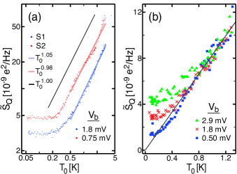
In the first part of the study, Exp. A, we measured for devices S1 and S2 (in separate runs) while increasing from to around over a period of 18 to 19 hours. We biased each SET at the voltage where its charge modulation is at a maximum. Immediately before each noise spectrum measurement, we acquired a gate modulation trace [Fig. 1(b), inset], extracted the minimum and maximum current, and set the current at the midpoint between these values by adjusting the gate voltage. For each SET, we acquired data at temperature points, with each spectrum averaged 250 times.
The noise data, displayed in Fig. 3(a), clearly show that increases linearly with temperature: The slopes in the logarithmic plot are and for S1 and S2, respectively. Other samples, not presented here, showed similar linear scaling with . This scaling is in contrast with the dependence presented by Kenyon et al. Kenyon et al. (2000) and Astafiev et al. Astafiev et al. (2006), although the latter group has observed in other devices Astafiev (2011).
At temperatures below about we observe a saturation of the noise, as reported by previous authors Wolf et al. (1997); Song et al. (1995); Li et al. (2007); Henning et al. (1999); Krupenin et al. (2000); Kenyon et al. (2000); Astafiev et al. (2006). The noise level becomes completely independent of in this regime to within our measurement precision; see discussion below.
III.2 Bias and temperature dependence of the noise
In Exp. B, we repeated the temperature sweep of Exp. A for device S1 from to over a period of 8 hours, while alternating the bias voltage of the SET between the three values shown with colored symbols in Fig. 1(d). For each data point, the spectrum was averaged 100 times. The noise data, plotted in Fig. 3(b), clearly show that the saturation levels at low depend on the bias voltage, which is consistent with a picture of TLFs activated by hot electrons in the SET.
As an alternative to SET self-heating, it has been proposed that electrons tunneling through the junctions supply energy directly to the TLFs, either by scattering inelastically with TLFs located inside the junction barriersKenyon et al. (2000), or by coupling to the electric field generated by the SET shot noiseWolf et al. (1997). In such processes, the tunneling electrons would be able to activate TLFs with energies up to , and a much larger number of TLFs would be activated for the highest value of than for the lowest one. This difference should persist as increases, until all TLFs can be thermally activated. On the contrary, we see that the bias dependence of TLF activation vanishes at [Fig. 3(b)]. We conclude from this result that such direct activation mechanisms cannot explain the bias dependence of .
In the regime , we see a clear linear dependence with . Using this relation, as we see in the following section, we can calculate the saturation temperature of the TLF ensemble for each of the three bias points.
III.3 Bias dependence of the noise at base temperature
To investigate in greater detail the connection between charge noise and bias voltage and current found in Exp. B, we performed Exp. C for S1, in which we measured the low-temperature saturation level of the charge noise at 315 bias points, each with a different value of and [Fig. 1(d)]. Each spectrum was averaged 100 times. The total measurement time was 12.6 hours, and the bias points were applied in random order to avoid any influence of measurement drift on the data.
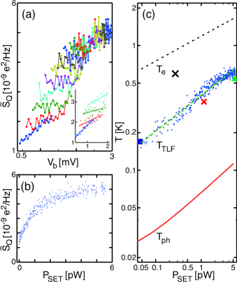
Figure 4(a) shows the charge noise level as a function of SET bias voltage , with lines connecting points with the same bias current . It is clear from this plot that increases with both and .
Plotting the noise data of Fig. 4(a) versus instead of , we see a smooth, monotonic increase in the noise with , but with a dependence much weaker than linear [Fig. 4(b)]. This indicates that the TLFs are heated by the power dissipated in the SET. The weak power law is characteristic of electron-phonon thermalization, which is generally assumed to explain the power dependence of the electron temperature in the SET islandKautz et al. (1993); Korotkov et al. (1994); Verbrugh et al. (1995); Meschke et al. (2004).
In Fig. 4(c), we have used the proportionality constant determined in Exp. B to calculate the equivalent temperature of the TLFs, , using the same noise data as in Figs. 4(a) and (b). The data are fitted with a line in the logarithmic plot [Fig. 4(c), dashed green] to yield . The three saturation temperatures extracted from Exp. B are plotted on the same scale. Since Exps. B and C were carried out more than one week apart, it is not unreasonable to expect the noise sources to have reconfigured somewhat, as commonly seen in experiments on low-frequency noise. Nonetheless, the two data sets agree rather well.
IV Thermal modeling
The current flowing through a SET dissipates power in the electron gas of both the island and the leads. The electrons on the island generally relax rapidly to a Fermi distribution, and these hot electrons may subsequently thermalize via preferential tunneling from the island and by emission of energy as phonons.
Since this self-heating affects the SET current in a theoretically predictable way, we can extract a value for the electron temperature of the island from the - characteristics of the SET.
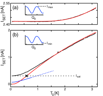
Along with each noise spectrum acquired in Exp. A, we measured the gate modulation curve of SET S1 [Fig. 1(b), inset]. Both the maximum and minimum of each such curve ( and ) depend on the electron temperature , as shown in Fig. 5.
By fitting the standard (Orthodox) model for the SET modelAverin and Likharev (1991) to versus , we can accurately extract the charging energy of the SET, as well as the exact value of the bias voltage . The extracted value for agrees with that obtained from - characteristics measured at base temperature. Using these parameters, we can compare the temperature dependence of with the Orthodox model. We find that the data and theory agree well for high , but that saturates at low , to a value which is substantially higher than theory predicts. We also calculate the total current using the analytical method of KönigKönig (1998). This treatment includes co-tunneling, but only considers two charge states on the SET island. Thus, this method is valid only for low values of and , and in this regime we find that the co-tunneling current is much too low (by a factor of ) to account for . The cross-over temperature between the experimental curve and the Orthodox curve provides the experimental value at , as shown in Fig. 5(b). This data point is also shown as a cross in Fig. 4(c).
Widely used models predict the electron-phonon thermalization power to follow with ranging approximately between 4 and 6, depending on geometry, temperature, and material propertiesWellstood et al. (1994); Meschke et al. (2004); Schmidt et al. (2004); Savin et al. (2006); Underwood et al. (2011). In this equation, is a material-dependent electron-phonon coupling coefficient, is the volume of the electron gas, and and are the temperatures of the electrons and the phonons, respectively. UsingMeschke et al. (2004) and for Al, we obtain an estimate of over the whole range of applied SET power [Fig. 4(c)]. The experimental data point [black cross in Fig. 4(c)] is within a factor 1.6 of the theoretical model [black dashed line in Fig. 4(c)], and we attribute the discrepancy to the relative simplicity of the electron-phonon thermalization model and the uncertainties in its input parameters. Qualitatively, we see that and the theoretical have similar dependencies on .
We observe no increase in at fixed SET bias for [Fig. 3(a)]. At these low temperatures, we expect on the SET island to be dominated by self-heating, while the electron gases of the leads are commonly believed to have temperatures close toKautz et al. (1993) . Geometrically, about as many of the TLFs contributing to are located adjacent to the SET leads as to the island [Fig. 2(d)]. On this assumption, one-half of the TLFs (those that predominantly thermalize with the leads) should contribute charge noise proportional to . In the regime of low , these TLFs would produce a slope in vs of . It is clear from Fig. 3(a) that this is not the case in our experiment. The electrons close to the junctions appear to follow the electron temperature on the SET island. We attribute this to local heating of the electrons in the leads closest to the junctions. This is plausible since the power dissipation, , in each of the leads takes place close to the junctions in comparison with the distance over which the electrons thermalize.
The electron-phonon coupling is usually assumed to be the dominant thermalization bottleneck for the island electrons, so that , and we used this approximation to calculate the electron temperature above. Nonetheless, some experiments have shown that the thermal power flowing from a SET with can produce a measurable increase in temperature of devices deposited nearby on the same substrate Krupenin et al. (1999); Savin et al. (2006). Since we have no means to measure in the region around the SET, we calculate an estimate from a finite-element model. The model is axially symmetric, with the SET defined as a disc at the surface with the same area as the actual SET, and with the same layer structure as the actual substrate. We assume a refrigerator temperature and use established literature values for the temperature-dependent thermal conductivities of forKumar et al. (1985) Si and forPohl et al. (2002) , respectively. We assume that all the power dissipated in the SET island is emitted as phonons from the Al/, and treat the materials as bulk media. We find that the calculated at the hottest point in the model is much too low to account for the elevated temperature of the TLF ensemble [Fig. 4(c)]. The only mechanism for the TLFs to assume a higher temperature than the local phonons is via direct contact with the SET electrons.
V Conclusions
Analysis of our noise data yields new information on the processes responsible for charge noise in mesoscopic devices. We summarize the results of our investigation in four conclusions:
(i) We see clearly that the charge noise increases linearly with refrigerator temperature for high temperatures, and saturates for low temperatures to a value that depends on the SET bias.
(ii) In the regime of low refrigerator temperature, the dependence of the charge noise on SET bias voltage and current is compelling evidence that the TLF ensemble dominating the noise is activated by SET self-heating.
(iii) By our estimates, the temperature of the TLF ensemble is approximately five times higher than the local surface temperature of the substrate, and two to three times lower than the electron temperature of the SET, at refrigerator base temperature [Fig. 4(c)]. This indicates that the TLFs are in stronger thermal contact with the SET electrons than with the phonons in the substrate.
(iv) As Kenyon et al. have pointed outKenyon et al. (2000), it is difficult to see how double-well TLFs outside the SET would thermalize with the SET electron gas. On the contrary, a process by which the noise is generated by electrons tunneling between the SET island and local defects (such as localized MIGSs or metallic grains) would account naturally for this thermal coupling, and would also produce the dependence we observe [Fig. 2]. Since the electron shares its time between the SET metal and the external well, it is reasonable that the fluctuator has an equivalent temperature lower than that of the SET electrons, in agreement with our observations. Localized MIGSsChoi et al. (2009) are universally present in the interfaces between conductors and insulators, so that this model can be applied to both metallic and semiconducting devices. It is rather intriguing to think that localized MIGSs might well play a key role in both 1/f charge noise, where they provide a trap for electron tunneling to and from the Fermi gas in, say, a SET, and 1/f magnetic flux noise, where they provide localized sites for electrons undergoing spin reversals that couple flux into a SQUID or flux-sensitive qubit.
Finally, we emphasize that all data acquired at low refrigerator temperature pertain to a voltage-biased, normal-metal SET, implying that the TLFs producing the 1/f charge noise are necessarily out of thermal equilibrium. This is also the case in metrological charge pumps, but not for nondissipative devices, such as charge qubits and Quantum Capacitance ElectrometersPersson et al. (2010) (QCEs). It is, however, likely that the microscopic nature of the TLFs is the same in all cases, and a detailed description of the noise in one type of device will surely help the understanding of the noise observed in other devices. Our work implies that one should focus on the nature of the metal-insulator interface to shed light on the nature of the potential wells responsible for the charge noise.
Acknowledgements.
We are grateful to Vladimir Antonov, Oleg Astafiev, Jonas Bylander, Pierre Echternach, Frank Hekking, John Martinis, Eva Olsson, Kyle Sundqvist, and Dale Van Harlingen for useful discussions, and to Thilo Bauch and Joachim Lublin for assistance with equipment. JC gratefully acknowledges his appointment as Chalmers 150th Anniversary Visiting Professor. The work was supported by the Swedish Research council, the EU project SCOPE and the Wallenberg foundation. This research is based upon work supported in part by the Office of the Director of National Intelligence (ODNI), Intelligence Advanced Research Projects Activity (IARPA) (JC). The views and conclusions contained herein are those of the authors and should not be interpreted as necessarily representing the official policies or endorsements, either expressed or implied, of ODNI, IARPA, or the U.S. Government. The U.S. Government is authorized to reproduce and distribute reprints for Governmental purposes not withstanding any copyright annotation thereon.References
- Averin and Likharev (1991) D. V. Averin and K. K. Likharev, in Quantum Effects in Small Disordered Systems, edited by B. Altshuler, P. Lee, and R. Webb (Elsevier, Amsterdam, 1991).
- Fulton and Dolan (1987) T. A. Fulton and G. J. Dolan, Phys. Rev. Lett. 59, 109 (1987).
- Paladino et al. (2002) E. Paladino, L. Faoro, G. Falci, and R. Fazio, Phys. Rev. Lett. 88, 228304 (2002).
- Bylander et al. (2011) J. Bylander, S. Gustavsson, F. Yan, F. Yoshihara, K. Harrabi, G. Fitch, D. G. Cory, Y. Nakamura, J.-S. Tsai, and W. D. Oliver, Nature Phys. 7, 565 (2011).
- Kautz et al. (2000) R. L. Kautz, M. W. Keller, and J. M. Martinis, Phys. Rev. B 62, 15888 (2000).
- Covington et al. (2000) M. Covington, M. W. Keller, R. L. Kautz, and J. M. Martinis, Phys. Rev. Lett. 84, 5192 (2000).
- Bylander et al. (2005) J. Bylander, T. Duty, and P. Delsing, Nature 434, 361 (2005).
- Machlup (1954) S. Machlup, J. Appl. Phys. 25, 341 (1954).
- Dutta and Horn (1981) P. Dutta and P. M. Horn, Rev. Mod. Phys. 53, 497 (1981).
- Zimmerli et al. (1992) G. Zimmerli, T. M. Eiles, R. L. Kautz, and J. M. Martinis, Appl. Phys. Lett. 61, 237 (1992).
- Zorin et al. (1996) A. B. Zorin, F. J. Ahlers, J. Niemeyer, T. Weimann, H. Wolf, V. A. Krupenin, and S. V. Lotkhov, Phys. Rev. B 53, 13682 (1996).
- Zimmerman et al. (1997) N. M. Zimmerman, J. L. Cobb, and A. F. Clark, Phys. Rev. B 56, 7675 (1997).
- Brown et al. (2006) K. R. Brown, L. Sun, and B. E. Kane, Appl. Phys. Lett. 88, 213118 (2006).
- Kafanov et al. (2008) S. Kafanov, H. Brenning, T. Duty, and P. Delsing, Phys. Rev. B 78, 125411 (2008).
- Wolf et al. (1997) H. Wolf, F. J. Ahlers, J. Niemeyer, H. Scherer, T. Weimann, A. B. Zorin, V. A. Krupenin, S. V. Lotkhov, and D. E. Presnov, IEEE Trans. Instr. Meas. 46, 303 (1997).
- Song et al. (1995) D. Song, A. Amar, C. J. Lobb, and F. C. Wellstood, IEEE Trans. Appl. Supercon. 5, 3085 (1995).
- Li et al. (2007) T. F. Li, Y. A. Pashkin, O. Astafiev, Y. Nakamura, J. S. Tsai, and H. Im, Appl. Phys. Lett. 91, 033107 (2007).
- Henning et al. (1999) T. Henning, B. Starmark, T. Claeson, and P. Delsing, Euro. Phys. J. B 8, 627 (1999).
- Krupenin et al. (2000) V. A. Krupenin, D. E. Presnov, A. B. Zorin, and J. Niemeyer, J. Low Temp. Phys. 118, 287 (2000).
- Kenyon et al. (2000) M. Kenyon, C. J. Lobb, and F. C. Wellstood, J. Appl. Phys. 88, 6536 (2000).
- Astafiev et al. (2006) O. Astafiev, Y. A. Pashkin, Y. Nakamura, T. Yamamoto, and J. S. Tsai, Phys. Rev. Lett. 96, 137001 (2006).
- Starmark et al. (1999) B. Starmark, T. Henning, T. Claeson, P. Delsing, and A. N. Korotkov, J. Appl. Phys. 86, 2132 (1999).
- Xue et al. (2009) W. W. Xue, Z. Ji, F. Pan, J. Stettenheim, M. P. Blencowe, and A. J. Rimberg, Nature Phys. 5, 660 (2009).
- Ubbelohde et al. (2012) N. Ubbelohde, C. Fricke, C. Flindt, F. Hohls, and R. J. Haug, Nat. Commun. 3, 612 (2012).
- Kautz et al. (1993) R. L. Kautz, G. Zimmerli, and J. M. Martinis, J. Appl. Phys. 73, 2386 (1993).
- Simkins et al. (2009) L. R. Simkins, D. G. Rees, P. H. Glasson, V. Antonov, E. Collin, P. G. Frayne, P. J. Meeson, and M. J. Lea, J. Appl. Phys. 106, 124502 (2009).
- Louie and Cohen (1976) S. Louie and M. Cohen, Phys. Rev. B 13, 2461 (1976).
- Choi et al. (2009) S. K. Choi, D.-H. Lee, S. G. Louie, and J. Clarke, Phys. Rev. Lett. 103, 197001 (2009).
- Clarke and Braginski (2004) J. Clarke and A. L. Braginski, eds., The SQUID Handbook, Vol. 1: Fundamentals and Technology of SQUIDs and SQUID systems (Wiley-VCH, 2004).
- Korotkov (1994) A. N. Korotkov, Phys. Rev. B 49, 10381 (1994).
- Kafanov and Delsing (2009) S. Kafanov and P. Delsing, Phys. Rev. B 80, 155320 (2009).
- Weissman (1988) M. Weissman, Rev. Mod. Phys. 60, 537 (1988).
- Astafiev (2011) O. Astafiev, private communication (2011).
- Korotkov et al. (1994) A. N. Korotkov, M. R. Samuelsen, and S. A. Vasenko, J. Appl. Phys. 76, 3623 (1994).
- Verbrugh et al. (1995) S. M. Verbrugh, M. L. Benhamadi, E. H. Visscher, and J. E. Mooij, J. Appl. Phys. 78, 2830 (1995).
- Meschke et al. (2004) M. Meschke, J. P. Pekola, F. Gay, R. E. Rapp, and H. Godfrin, J. Low Temp. Phys. 134, 1119 (2004).
- König (1998) J. König, Quantum Fluctuations in the Single-Electron Transistor, Ph.D. thesis, Universität Karlsruhe (1998).
- Wellstood et al. (1994) F. C. Wellstood, C. Urbina, and J. Clarke, Phys. Rev. B 49, 5942 (1994).
- Schmidt et al. (2004) D. R. Schmidt, C. S. Yung, and A. N. Cleland, Phys. Rev. B 69, 140301 (2004).
- Savin et al. (2006) A. M. Savin, J. P. Pekola, D. V. Averin, and V. K. Semenov, J. Appl. Phys. 99, 084501 (2006).
- Underwood et al. (2011) J. M. Underwood, P. J. Lowell, G. C. O’Neil, and J. N. Ullom, Phys. Rev. Lett. 107, 255504 (2011).
- Krupenin et al. (1999) V. A. Krupenin, S. V. Lotkhov, H. Scherer, T. Weimann, A. B. Zorin, F.-J. Ahlers, J. Niemeyer, and H. Wolf, Phys. Rev. B 59, 10778 (1999).
- Kumar et al. (1985) G. S. Kumar, J. W. Vandersande, T. Klitsner, R. O. Pohl, and G. A. Slack, Phys. Rev. B 31, 2157 (1985).
- Pohl et al. (2002) R. O. Pohl, X. Liu, and E. Thompson, Rev. Mod. Phys. 74, 991 (2002).
- Persson et al. (2010) F. Persson, C. M. Wilson, M. Sandberg, and P. Delsing, Phys. Rev. B 82, 134533 (2010).