Charged States and Band-Gap Narrowing in Codoped ZnO Nanowires for Enhanced Photoelectrochemical Responses
Abstract
By means of first-principles calculations within the density functional theory, we study the structural and optical properties of codoped ZnO nanowires and compare them with those of the bulk and film. It is disclosed that the low negative charged ground states of nitrogen related defects play a key role in the optical absorption spectrum tail that narrows the band-gap and enhances the photoelectrochemical response significantly. A strategy of uncompensated N, P and Ga codoping in ZnO nanowires is proposed to produce a red-shift of the optical absorption spectra further than the exclusive N doping and to get a proper formation energy with a high defect concentration and a suppressed recombination rate. In this way, the absorption of the visible light can be improved and the photocurrent can be raised. These observations are consistent with the existing experiments, which will be helpful to improve the photoelectrochemical responses for the wide-band-gap semiconductors especially in water splitting applications.
pacs:
73.20.Hb, 73.21.Hb, 78.20.BhI Introduction
ZnO is a semiconductor with wide band-gap, and is stable in aqueous solution. One of the most remarkable applications of ZnO in photoelectrochemical (PEC) field is that, it can be used to split water by solar light to produce hydrogen as clean fuel. Besides, ZnO is also a promising candidate of photoanode material in PEC cells book . For most of wide-gap semiconductors such as ZnO and TiO2, the band-gap is far beyond the threshold of 1.23 eV for the water splitting, even though the overpotential looses require a larger threshold energy about 1.7 eV book-TiO2 . On the other hand, the wide band-gap semiconductors can merely absorb the ultraviolet portion of the solar spectra. To enhance the efficiency of utilizing the solar energy, a key issue is how to narrow the band-gap of semiconductors below 2.0 eV E-TiO2 so that the majority of the visible light can be absorbed. To solve this issue, a suitable band edge positioning with respect to the potentials of reduction and oxidation reactions, together with the suppression of charge recombination centers, should be considered book .
There has been a number of studies concerning the above considerations. Among them, the donor-acceptor codoping in ZnO and TiO2 materials is remarkable. Recent theoretical calculations show that, it is possible to narrow the band-gap of ZnO bulk by codoping (Ga+N) or (Al+N) ZnO3N+Ga ; the band-gaps of TiO2 bulk can be narrowed to be 2.26 eV, 1.6 eV and 0.9 eV for charge compensated codoping (Mo+C) TiO23Mo+C , noncompensated codoping (Cr+N) and (V+C) TiO23Cr+N , respectively. Experimentally, doping Cu ZnO2Cu and codoping (Ga+Cu) ZnO2Ga+Cu in p-type, codoping (Ga+N) ZnO2Ga+N or (Al+N) ZnO2Al+N in n-type ZnO films have been realized. In their optical absorption spectra, there is a long tail from the absorption peak in the ultraviolet range that persists in the central visible range, thereby narrowing the band-gap. The key factors to enhance the PEC responses by codoping Ga and N in ZnO films are believed to include either producing an excellent crystallinity, or to narrow the band-gap, or to generate a wide depletion layer to suppress the recombination rate ZnO2Ga+N . It is also observed that N doped n-type ZnO nanowires (ZnONWs) E-ZnO1N can enhance PEC responses that are similar to those in codoped ZnO films. A theoretical study on the O-vacancy in ZnONWs suggests that the neutral and charged states of defects have crucial contributions to optical absorption in the visible range ZnO1Ov . The charged states of O-vacancy in TiO2 bulks have also been emphasized TiO23Ov1 ; TiO23Ov2 .
In this paper, we shall explore the structural and optical properties of uncompensated N, P and Ga codoped ZnONWs by means of the first-principles calculations within the density functional theory (DFT) DFT . We have found that the low negative charged states of N-related defects play a key role in producing the long tail of the optical absorption spectrum, which narrow the band-gap and enhance the PEC response significantly. It is also observed that the uncompensated N, P and Ga codoping can generate a red-shift of the optical absorption spectra larger than the exclusive N doping, and a proper formation energy with a high defect concentration and a suppressed recombination rate can be acquired. These observations will be useful for the application of ZnONWs in the PEC field (e.g. the water splitting).
This paper is organized as follows. In Sec. II, we shall briefly introduce the calculational approach, including the generalized gradient approximation plus U (GGA+U) correction, and the extrapolation method to correct the band-gaps. In Sec. III, the negative charged states and optical absorption spectra of N-doped ZnONWs will be explored. In Sec. IV, the defect bands and uncompensated N, P and Ga codoping in ZnONWs to enhance the PEC response will be discussed. An extrapolation method is applied to discuss the relevant experimental observations. Finally, a summary is given.
II Calculational Approach
The calculations are performed using the DFT based VASP code VASP , which employs the pseudopotentials of the projector augmented wave (PAW) PAW , with the GGA in the Perdew-Burke-Ernzerhof (PBE) form PBE for exchange correlations. The cutoff energy for the plane-wave basis set is 400 eV. The convergence criteria for DFT calculations are 10-4 eV of total energy and 10-3 eV/Å of force. All structural relaxations and formation energies are calculated with spin polarization, with the Morkhorst-Pack k-points meshes of , and for ZnO bulk, ZnO film and ZnONW, respectively. After a full relaxation, the density of states (DOS) and the optical absorption spectra of ZnONW are calculated without spin polarization, and the k-points mesh is raised to .
To obtain the absorption spectra, the frequency dependent dielectric matrices are calculated by VASP after structural relaxation. The real and imaginary parts of the dielectric tensor are obtained by the usual Kramers-Kronig transformation and a summation over empty states, respectively optical , from which the energy dependent dielectric function along the axial direction of the nanowires and thus the imaginary part of refractive index can be obtained. The optical absorption intensity is proportional to the imaginary part of refractive index.
It is known that the conventional DFT method always underestimates the band-gap of semiconductors, and the position of the charged states of the defects with respect to the valence band edge also tends to be underestimated. The character of the defect bands is a mixture of the valence and conduction bands, which can be reflected by the change of the defect bands from GGA to GGA+U calculations extrapolation . Note that in the following, Figs. 2-6 are calculated by GGA without U correction, while for Fig. 7, the GGA+U method U implemented in VASP code is employed to calculate the optical absorption spectra for several key cases. Dudarev’s approach Dudarev is adopted, where only the difference of the Coulomb and exchange parameters is meaningful.
Inspired by the extrapolation scheme in previous works about ZnO extrapolation ; extrapolation0 , based on the results from both GGA and GGA+U with a small value of for d electrons, we extrapolate the calculated band-gap of the ground state of N doped ultrathin ZnONW to the band-gap of the experimentally synthesized N doped ZnONW E-ZnO1N , and then estimate the band-gaps and the optical absorption peaks if other defects are doped in the same ZnONWs in experiments. The extrapolation equation that is similar to the one given in Ref. extrapolation, is as follows:
| (1) |
where represents substitutionally doping one N atom instead of O atom, and represents other defects. Any band-gap corresponds to a peak in the optical absorption spectrum, no matter how it is obtained either from GGA () and GGA+U (), or from the experiment ().
Besides the extrapolation method to correct the band-gap, it is instructive to note that by incorporating U not only for d electrons but also for s or p electrons, the effective corrections to the band-gaps and spectra have already been obtained in several cases ZnO1Ov ; TiO23Ov2 ; ZnO3Ov . To aim at giving an approximate but intuitive view on the absorption spectra, we shall consider several situations for a comparison in the following [as will be seen in Figs. 7(a) and (b)], namely, U is incorporated for the d electrons of Zn, p electrons of O ZnO1Ov , as well as the corresponding electrons of their substitutional dopants.
In a supercell, the formation energy of a charged defect with a net charge can be calculated through the following equation formation1 ; formation2 ; TiO23Ov1
| (2) |
where and are the total energy with and without the defects, respectively, is the change of atomic number, is the reservoir chemical potentials, Zn, O, N, P, Ga, and is the Fermi level (FL) with respect to the valence band edge varying between zero and the band-gap .
For charged defects, a jellium background is used. However, we note that the periodic boundary conditions may induce spurious electrostatic interactions between charged unit cells, possibly leaving errors in energy from the first-principles calculations PBC . For an aperiodic three-dimensional condensed matter system, Makov and Payne evaluated the total energy by PBC
| (3) |
where , , , , , and is the desired electrostatic energy of the point defect in the dilute limit, the ionic charge of the defect, the Madelung constant of the lattice, the linear dimension of the supercell, the dielectric constant, and the quadrupole moment independent of , respectively. The term is the Madelung energy for the lattice of point charges in the jellium background, and for quasi one-dimensional system such as nanowires, corresponds to the periodicity of the nanowire 1DPBC1 . The term exists with a quadrupole moment and is inversely proportional to the supercell volume PBC . If the vacuum separation between the nanowires is fixed and only the axial length of supercell changes, the supercell volume is proportional to . More methods to correct the formation energy have been demonstrated 1DPBC1 ; 1DPBC2 for several cases of nanowires.
In the present work, to evaluate the effect of the energy errors on the structural stability, we model the energy correction term similar to the form of Madelung energy. The total energy is expressed as
| (4) |
where is the parameter and is zero for neutral charged nanowires, and is the axial length of the supercell. Then, Eq. (2) is corrected to be
| (5) |
| (6) |
is the desired energy of the defect in the dilute limit. For a given charged defect with given and , and the parameter of the defect can be obtained by calculating (,) with an axial length of different unit cells, and then linearly fitting fitting (,) to the inverse of . Thus, the error of the defect formation energy (,) can be evaluated by
| (7) |
The supercells of ZnO bulk, ZnO film and ZnONW contain 128, 144, 96 atoms in total, respectively. The ZnO film is modeled perpendicular to the axis along the [110] direction, containing 9 central-symmetric layers, 13.3 Å thick. The central three layers are fixed to the bulk positions while the top and bottom three layers are allowed to relax without constraints. The supercell of ZnONW contains two periodic units along the [0001] direction with diameter of 9.9 Å, and the axial length of the supercell is 10.84 Å. The vacuum distances between the surfaces of neighboring ZnO film and ZnONW are kept 9.7 and 15.1 Å, respectively. The size of the supercell of ZnONW is Å. The lengths of these three supercells of ZnO bulk, ZnO film and ZnONW are marked by , and , respectively. For each case, , and represent the unit lengths of the axial directions, and represents the given length of supercell in the direction with vacuum. By default, these supercells are used to calculate the formation energies (,=2) directly by Eq. (2).
To evaluate the error of the defect formation energy (,2) by Eq. (7) and the linear fitting method fitting , the total energies of a supercell of ZnO bulk, a supercell of ZnO film, and supercells of ZnONW are also calculated. The influence of the energy error (,2) will be analyzed in the context.
III Negative Charged States of N-doped ZnO Nanowires
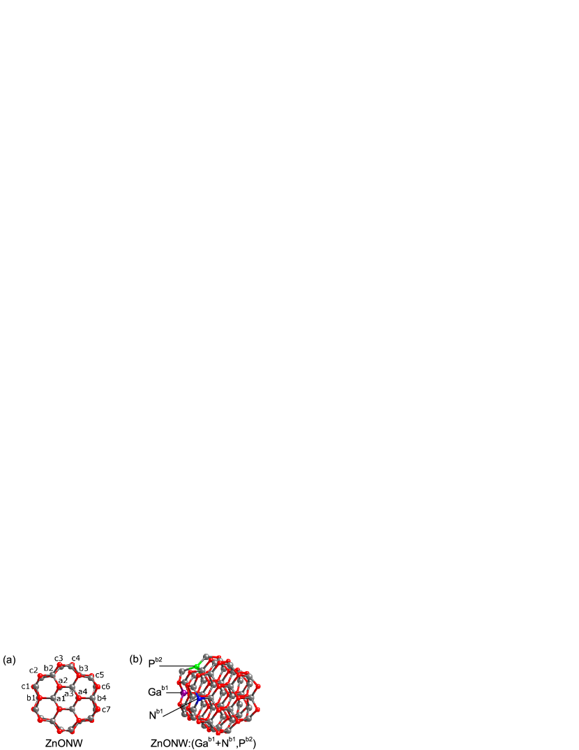
The structure of the defect free ZnONW is shown in Fig. 1(a), where several doping positions are marked. To investigate the properties of the defects in the supercell of ZnONW with two periodic units, for every position only one of the two units is substitutionally doped in order to avoid two same dopants occupying the same position. As an example, ZnONW with Ga, N and P dopants at , and positions, respectively, is shown in Fig. 1(b), marked as ZnONW:(Gab1+Nb1,Pb2), where (Gab1+Nb1) represents that a pair of Ga and N dopants at are bonded with each other. Ga substitutes Zn atom, N and P substitute O atoms, respectively.
| position of defect | (eV) | ||
|---|---|---|---|
| 4.87 | |||
| 4.72 | |||
| 4.73 |
| positions of defects | (eV) | ||
|---|---|---|---|
| 9.37 | |||
| 9.39 | |||
| 9.52 | |||
| 9.61 | |||
| 9.53 | |||
| 9.55 |
To compare the stability of the structures with different defects, the formation energies are calculated. For the defect in the ZnONW supercell (ZnONW:N), all , and positions are equivalent, respectively. The formation energies are listed in Table I. The difference of between ZnONW:Nb1 and ZnONW:Nc1 is 0.01 eV, while of ZnONW:Nb1 and ZnONW:Nc1 are lower than that of ZnONW:Na1 by at least 0.14 eV. For all of these cases the total magnetic moment per supercell after full relaxation is found to be 1.000 . It indicates that the surface () and subsurface () sites are energetically favorable for the defect. For doping two N atoms in the supercell (ZnONW:2N), of several selected cases are shown in Table II. Among these cases, ZnONW:2Nb1c1 is energetically the most favorable. These results are in general agreement with the results of a previous work ZnO1N . In the following, only ZnONW:Nb1 and ZnONW:2Nb1c1 are discussed as typical examples with one or two doped N atoms in the ZnONW, if not specified. For a few interesting cases, more than one configurations of energetically favorable defects with nearly the same will be considered.
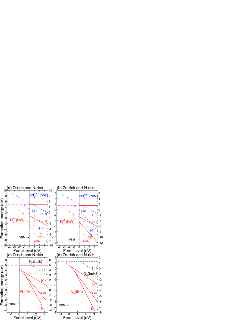
Based on Eq. (2), of ZnONW:Nb1 and ZnONW:2Nb1c1, and doping one N atom in the supercells of ZnO bulk and film in different charged states are shown in Figs. 2(a) and (b), (c) and (d), respectively, where the negative range under the Fermi level (FL) corresponds to the valence band. As the FL moves from the valence band maximum (VBM) to the conduction band minimum (CBM), the semiconductor changes from p-type to n-type. In Fig. 2, as the band-gap gives the upper limit of the FL, the band-gap of ZnO bulk is taken as the experimental value of 3.43 eV U-ZnO3 , while the band-gaps of ZnO film and ZnONW are approximately set to 3.45 and 3.70 eV, respectively.
For ZnO bulk, the (0/-1) charge transition of defect is deep in the gap, in agreement with the previous observation p-ZnO . On the other hand, the (0/-1) charge transition of ZnO film happens below the VBM; more than five transitions to negative charged states of ZnONW appear within the valence band. It is reported both experimentally and theoretically that the band of surface O 2p dangling bond of ZnO sits below the VBM. surface1 ; surface2 This may be true for low dimensional ZnO but not for all metal-oxide semiconductors surface3 . So, the charge transition points below VBM in Fig. 2 correspond to the unoccupied surface states in the ultrathin ZnO film and ZnONW. As a result, in contrary to bulk, in ZnO film and ZnONW have many negative charged states in the band-gap, especially under n-type condition with the FL close to the CBM. These negative charged states are easier to get negative than ZnO bulk.
However, not all of these negative charged states are stable. For ZnONW and n-type ZnO film, as the defect carries more negative charge, the variation of for adding one more negative charge becomes smaller rapidly. When the energy difference between different charged states is smaller than the energy lowering for producing a Zn vacancy () with the same negative charge, it will induce spontaneous disintegration from higher negative states into lower negative states and defects DinTiO2 . The most stable state of is -2 charged () in spite of O-rich, Zn-rich, p-type and n-type conditions. For ZnO film, is -0.76, -7.66, 2.81 and -4.09 eV for O-rich p-type, O-rich n-type, Zn-rich p-type and Zn-rich n-type extremes, respectively. For ZnONW, these values are -6.48, -13.86, -3.13, and -10.51 eV, respectively. An approximate criterion to filter the unstable charged states of can be written as
| (8) |
If the above inequality is satisfied, the charged state will be unstable; otherwise the charged states are relatively stable without self-disintegration, as shown in Fig. 2.
For ZnONW:Nb1 and ZnONW:2Nb1c1, as manifested in Figs. 2(a) and (b), the relatively stable states free from the spontaneous disintegration include the neutral and -1 charged states under the O-rich condition, and 0-2 charged states under Zn-rich condition, among which the ground state in energy is -1 charged under O-rich condition and -2 charged under Zn-rich condition, respectively. In general, under the O-rich condition is larger than that under the Zn-rich condition and, it is easier to get a ground state with a higher negative charge under the Zn-rich condition than that under the O-rich condition. It is evident that ZnONW:2Nb1c1 has a larger than ZnONW:Nb1.
The negative charged states with negative play roles as acceptors to compensate electrons, resulting in high compensation rate and low photocurrent. The equilibrium concentration of a defect at temperature is given by formation1 ; formation2
| (9) |
Obviously, a larger positive leads to a lower defect concentration, and for a negative , the defect can be viewed as an active compensation center. So, a small positive of the ground state is preferred, which leads to a high defect concentration and a low recombination rate. To meet this requirement, among the ground states of ZnONW:Nb1 and ZnONW:2Nb1c1, under the O- and N-rich environments of ZnONW:(N at p-type extreme and ZnONW:(2N at n-type extreme are favorable, whose are 0.67 and 1.73 eV, respectively.
The defect energy errors of the charged states are evaluated by Eqs. (5) and (7) with the linear fitting method. [(N)1-,2] is found to be -0.43 eV, and the corresponding parameter is 4.94 eVÅ. It means that after the energy correction, in Fig. 2(a), of ZnONW:(Nb1)1- under O- and N-rich environments at p-type extreme drops from 0.67 eV to 0.24 eV. Moreover, [(N)2-,2] is -1.48 eV, with the parameter of 15.50 eVÅ; [(VZn)2-,2] is -1.41 eV, with of 15.27 eVÅ. Substituting these three values of into (8), this inequality is still satisfied. So, under the O- and N-rich environments, the -1 charged state of ZnONW:Nb1 is still the ground state, and at p-type extreme of 0.24 eV will also lead to a high defect concentration and a low recombination rate. It can be seen that as the negative charge increases from -1 to -2, of ZnONW:Nb1 is enlarged from -0.43 eV to -1.48 eV. For the -3 charged state of ZnONW:Nb1, is expected to be corrected downward by more than 1.48 eV, and it may turn from the unstable state to stable state under the Zn- and N-rich environments in Fig. 2(b). However, the -3 charged state is less important and has no influence on the water splitting. Similarly, after an energy correction, although of ZnONW:(2Nb1c1)1- is lowered by a fraction of one electron volt, ZnONW:(2Nb1c1)1- under O- and N-rich environments at n-type extreme is still the only state of ZnONW:2Nb1c1 favorable for the water splitting.
As a comparison, the charged states of ultrathin ZnO film are also discriminated by the same criterion in inequality (8), as shown in Figs. 2(c) and (d). Except for the narrow range near the n-type extreme under the O-rich environment, the ground state of defect in ZnO film is highly negative charged with a negative , which is easy to lead to a high recombination rate. If can be lifted from negative to positive, it would suppress the recombination rate and raise the photocurrent. Normally, the passivated codoping could lead to a larger than the single doping, as evidenced by the experimental observation that (Ga+N) codoped ZnO films have a significantly enhanced photocurrent and a suppressed recombination rate than the solely N doped ZnO film ZnO2Ga+N . The present analysis is effective to explain the experimental phenomena for both ZnONW and ZnO film. For the -1 charged state, from Eq. (7) is -0.50 and 0.21 eV for ZnO film and bulk, respectively. However, such energy errors will not alter the conclusions for ZnO film and bulk.
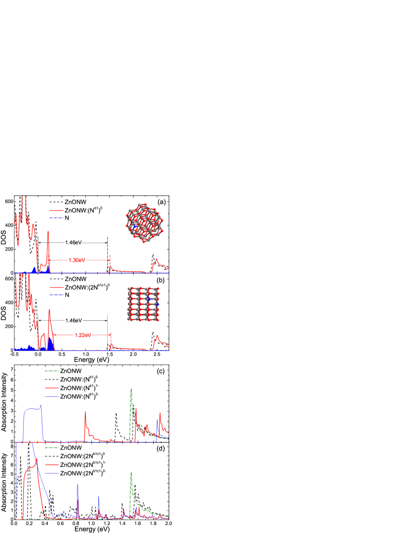
Fig. 3 shows the DOS and optical absorption spectra of ZnONW:Nb1 and ZnONW:2Nb1c1. For both cases, the partial DOS (PDOS) of N in Figs. 3(a) and (b) reveals that the valence electrons of N dopants accumulate at the top of the valence band, resulting in a group of defect bands above the VBM of pure ZnONW. Compared with the pure ZnONW, the band-gaps of ZnONW:Nb1 and ZnONW:2Nb1c1 are narrowed by 0.16 and 0.24 eV, respectively.
Figs. 3(c) and (d) present the optical absorption spectra of ZnONW:Nb1 and ZnONW:2Nb1c1 with different charged states, respectively, in comparison with the pure ZnONW. It is noticeable that even for the negative charged states in Figs. 3(c) and (d), the defect bands in the band-gap are not so close to the CBM as the gap is smaller than 0.5 eV. In fact, the spectra of the negative charged states in the range of 0.0-0.5 eV are contributed by the electron transition from the main valence bands to the defect bands, or within the defect bands between the VBM and CBM. So are the spectra of neutral ZnONW:(N from 0.00 to 1.30 eV, and the spectra of neutral ZnONW:(2N from 0.00 to 1.22 eV. For the application in the PEC water splitting, only the electron transition from the valence bands into the conduction bands is meaningful and effective. Thus, such spectra in the range close to 0.0 eV are ineffective, and will not be discussed. Focusing on the remaining part of the spectra, the spectra of -1 charged ZnONW:Nb1, -1 and -2 charged ZnONW:2Nb1c1 have red-shifts more remarkable than those of either their neutral charged states or the pure ZnONW. A common ground of these low negative charged states is that their total charges are no larger than that of the corresponding defect-free nanowires.
Moreover, by incorporating the results from Figs. 2(a) and (b), we find that ZnONW:(N at p-type extreme and ZnONW:(2N at n-type extreme under the O- and N-rich environments are the two most probable states of the ultrathin ZnONW with defects to perform a nice PEC response. These two states are ground states with proper formation energies on one hand, and have the optical absorption spectra with significant red-shifts on the other hand. If the spectra of neutral charged ZnONWs remain in the range of ultraviolet light, only these negative charged states are possible to red-shift the spectra into the visible range, leaving a series of absorption peaks from the ultraviolet to visible range.
It is intriguing to note that for N doped n-type ZnONW for PEC water splitting, the optical absorption spectrum was experimentally observed to leave a long decaying tail from the ultraviolet to visible range, where the tail absorbance at 500 nm is approximately the half of the main absorption peak at 400 nm E-ZnO1N . In experiments it was identified that the dominating defect in ZnONW is , with the N concentration of 3.7% E-ZnO1N . Comparing this experiment to our theoretical results of ZnONW:Nb1 and ZnONW:2Nb1c1, we deduce that the experimentally observed spectrum with a tail stretching into the visible range can be attributed to the negative charged ground states of .
IV Uncompensated Codoping of (Ga, N, P) in ZnO Nanowires
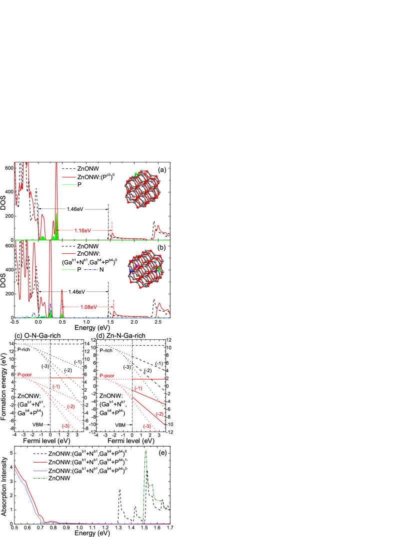
To consider the case of defect in ZnONW (ZnONW:P), as the position is energetically favorable for , ZnONW:Pc3 is chosen as an example to investigate the general properties of ZnONW:P. Fig. 4(a) shows that the defect bands of P situate deeper than N in the band-gap of pure ZnONW, giving rise to a sharp peak of DOS, and the band-gap is narrowed from 1.46 eV of the pure ZnONW to 1.16 eV. Aiming at narrowing further the band-gap, it is conceived that N and P are codoped into ZnONWs. Combining the characteristics of N and P dopants, the band-gap may be narrowed remarkably by P while the DOS of the defect bands is maintained to spread from the VBM as continuously as possible by either N or P dopants. Accordingly, by incorporating the advantages of passivated codoping by keeping the crystallinity, controlling the formation energy, and suppressing the recombination rate ZnO2Ga+Cu ; ZnO2Ga+N , we try to codope one (Ga+N) and one (Ga+P) in pair per supercell into ZnONWs [ZnONW:(Ga+N,Ga+P)].
To examine the above consideration, as an example, the DOS, formation energy and optical absorption spectrum of ZnONW:(Gab1+Nb1,Gab4+Pb4) are calculated, as presented in Figs. 4(b)-(e). From Fig. 4(b), one may see that the band-gap of ZnONW:(Gab1+Nb1,Gab4+Pb4) is narrowed to 1.08 eV, which is smaller than that of ZnONW:Pc3. Meanwhile, the gap between the deepest P defect bands and the lower defect bands of N and P is kept quite narrow.
could be manipulated by the chemical potential of P () between the values of P-rich and P-poor PN-ZnO , where it is known that the most P-rich potential of is calculated from P4O10 formation2 , and we choose P4 to obtain a P-poor approximately. Figs. 4(c) and (d) show that under the O-rich condition none of the negative charged states of ZnONW:(Gab1+Nb1,Gab4+Pb4) is stable, and the ground state is neutral charged [ZnONW:(Gab1+Nb1,Gab4+Pb4)0] with a positive , whereas under the Zn-rich condition the ground state is -2 charged [ZnONW:(Gab1+Nb1,Gab4+Pb4)2-] with a negative at n-type extreme. However, in Fig. 4(e), the optical absorption spectra of -1 and -2 charged states have no effective red-shifts from the neutral charged state that can narrow the gap between the defect bands and the CBM. This is because either -1 or -2 charged state of ZnONW:(Gab1+Nb1,Gab4+Pb4) has a total charge larger than that of the defect-free nanowire. Therefore, no matter whether the formation energy is corrected by Eq. (7) or not, ZnONW:(Ga+N,Ga+P) is not so useful for the water splitting.
| positions of defects | ||
|---|---|---|
| 15.78 | ||
| 15.75 | ||
| 15.80 | ||
| 15.78 | ||
| 16.2 | ||
| 16.2 | ||
| 16.2 | ||
| 20.1 | ||
| 16.1 | ||
| 16.1 | ||
| 16.3 | ||
| 16.2 | ||
| 16.3 | ||
| 16.4 |
To improve the performance, it turns out to take advantage of the low negative charged ground state with a total charge equal to the defect-free nanowire, as is in the case of ZnONW:Nb1. A strategy can be proposed to promote the PEC responses of ZnONWs by means of the uncompensated codoping of one (Ga+N) in pair and one single P dopant per supercell [ZnONW:(Ga+N,P)]. for several ZnONW:(Ga,N,P) cases are listed in Table III. It is seen that the defects including a pair of (Gab1+Nb1) and one single P at or or or position are relatively the most favorable configurations in energy. The difference of between these four cases are so small that it is no larger than 0.05 eV. Comparing the cases of (Gab1+Nb1,P) and (Gab1+Pb1,N), one finds that the pair of (Gab1+Nb1) is energetically more favorable than (Gab1+Pb1). In presence of the (Gab1+Nb1) pair, the P dopants at positions are unstable, because in these cases is usually larger than 200 eV. The three typical examples such as ZnONW:(Gab1+Nb1,Pb2), ZnONW:(Gab1+Nb1,Pa2) and ZnONW:(Gab1+Nb1,Pb4) are energetically favorable, whose total magnetic moments per supercell after full relaxation are found to be 1.093, 1.158 and 1.146 , respectively.
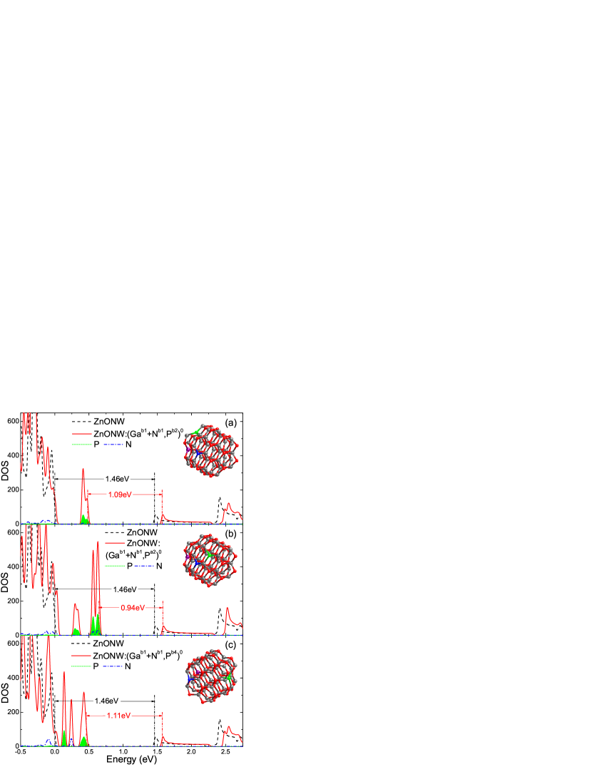
As shown in Figs. 5, all the band-gaps of these three cases are narrower than those of ZnONW:Nb1, ZnONW:2Nb1c1 and the pure ZnONW, but are close to the band-gap value of ZnONW:(Gab1+Nb1,Gab4+Pb4). For ZnONW:(Gab1+Nb1,Pa2) and ZnONW:(Gab1+Nb1,Pb4), there are also defect bands spreading between the VBM and the deepest defect peak of DOS.
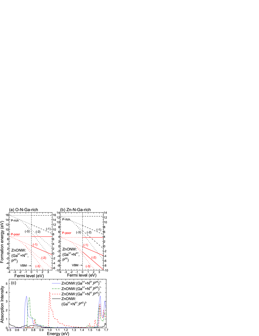
In Figs. 6(a) and 6(b), the ground states of ZnONW:(Gab1+Nb1,Pb2) under the O-rich and Zn-rich environments are -1 [ZnONW:(Gab1+Nb1,Pb2)1-] and -2 [ZnONW:(Gab1+Nb1,Pb2)2-] charged, respectively. of ZnONW:(Gab1+Nb1,Pb2)1- is -0.54 eV at n-type extreme under the O-, N-, Ga-rich and P-poor environments [Fig. 6(a)]; of ZnONW:(Gab1+Nb1,Pb2)2- is -0.94 eV at n-type extreme under the Zn-, N-, Ga- and P-rich environments [Fig. 6(b)]. For these two states, evaluating the formation energy error from Eq. (7), [(Gab1+Nb1,Pb2)1-,2] is -0.46 eV with the parameter of 4.99 eVÅ; and [(Gab1+Nb1,Pb2)2-,2] is -1.53 eV with of 15.88 eVÅ. Thus, after counting the correction on energy, changes from -0.54 eV to -1.00 eV, and from -0.94 eV to -2.47 eV. No matter with or without the energy correction, these two cases are kept to be in the ground states and can easily produce a small positive in the ground state by manipulating the n-type extreme and the chemical potential . They are energetically preferable for a high defect concentration and a low recombination rate. of ZnONW:(Gab1+Nb1,Pa2) and ZnONW:(Gab1+Nb1,Pb4) are similar to that of ZnONW:(Gab1+Nb1,Pb2) because of a very small difference among them.
Fig. 6(c) manifests that for ZnONW:(Gab1+Nb1,Pb4)1-, ZnONW:(Gab1+Nb1,Pb2)1- and ZnONW:(Gab1+Nb1,Pa2)1-, the leftmost absorption peak with an intensity larger than 1.0 lies at 0.72, 0.75 and 1.00 eV, respectively. Among them, the spectra of ZnONW:(Gab1+Nb1,Pb4)1- and ZnONW:(Gab1+Nb1,Pb2)1- have further red-shift from those of ZnONW:(Nb1)1- and ZnONW:(2Nb1c1)1-. The peaks around 1.62 eV correspond to the band-gap from the main VBM to the main CBM, in spite of the defect bands. In contrast, ZnONW:(Gab1+Nb1,Pa2)2- gives no efficient band-gap narrowing, so are the -2 charged states of the other two cases.
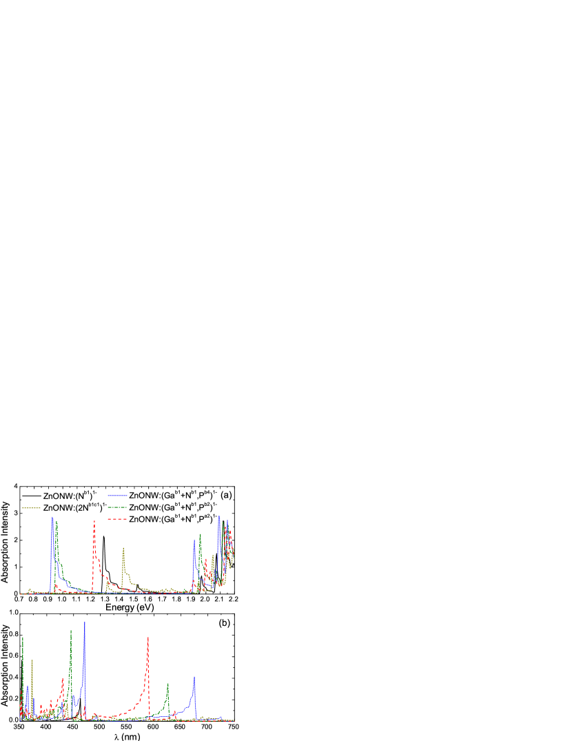
Due to the severe underestimation of band-gaps by the DFT, all the results above calculated within the GGA cannot quantitatively reflect the realistic situation in PEC responses. For this purpose, the GGA+U and extrapolation methods that are introduced in Section II are employed here. When U correction of =5.0 eV for the d electrons is added to the GGA calculation, the band-gaps and spectra are partially corrected, as shown in Fig. 7(a). For ZnONW:(Gab1+Nb1,Pb4)1-, ZnONW:(Gab1+Nb1,Pb2)1-, ZnONW:(Gab1+Nb1,Pa2)1-, ZnONW:(Nb1)1- and ZnONW:(2Nb1c1)1-, the leftmost absorption peak with an intensity larger than 1.0 lies at 0.93, 0.96, 1.22, 1.29 and 1.42 eV, respectively.
From the preceding results, we unclose that under the O-, N-, Ga-rich, P-poor and n-type environments, the uncompensated (Ga, N, P) codoping cases such as ZnONW:(Gab1+Nb1,Pb4)1-, ZnONW:(Gab1+Nb1,Pb2)1- and ZnONW:(Gab1+Nb1,Pa2)1- are energetically favorable, whose total charge is equal to that of the defect-free nanowire. In general, their optical absorption spectra have larger red-shifts and higher absorption peaks than the cases of exclusive N doping. Meanwhile, the (Ga, N, P) codoping cases have proper formation energy that can lead to a high defect concentration and a low recombination rate. Both factors are much favored in enhancing the photocurrent in the PEC water splitting.
To show the improvement of the uncompensated codoping of (Ga, N, P) compared with the exclusive N dopoing in the ZnONWs, in a way approaching to the experiment, an approximate estimation is performed by utilizing the extrapolation equation (1). The calculated results by GGA and GGA+U with a of 5.0 eV for d electrons can be extrapolated to the experimental ones. ZnONW:(Nb1)1- is taken as the standard defect of in Eq. (1), and is about 3.11 eV, which corresponds to the red-shifted peak of the N doped ZnONW at about 400 nm in the UV-vis spectra in the experiment E-ZnO1N . Consequently, the resulted of ZnONW:(Gab1+Nb1,Pb4)1-, ZnONW:(Gab1+Nb1,Pb2)1- and ZnONW:(Gab1+Nb1,Pa2)1- is 1.96, 1.99 and 2.30 eV, corresponding to 633, 623 and 540 nm, respectively.
Besides the extrapolation method, to give another direct and intuitive illustration, U correction can be added for both d and p electrons. When is assumed as 18.0 eV for d electrons and 15.0 eV for p electrons, respectively, the long-wavelength end of the optical absorption spectra of the exclusive N doping is manipulated to stop just at the range of violet and blue light, which is close to the experiment E-ZnO1N . Such a setting of GGA+U focuses on directly correcting the band-gap to approach the experimental value, while the expense is that, the inner band structures are disturbed more greatly than the extrapolation method with a small U added only for d electrons. As shown in Fig. 7(b), at the long-wavelength end of the spectra of ZnONW:(Nb1)1- and ZnONW:(2Nb1c1)1-, the last peak with an absorption intensity larger than 0.1 locates at 463 and 438 nm, respectively. In contrast, the last peak with an absorption intensity larger than 0.3 of ZnONW:(Gab1+Nb1,Pb4)1-, ZnONW:(Gab1+Nb1,Pb2)1- and ZnONW:(Gab1+Nb1,Pa2)1- locates at 675, 623 and 589 nm, respectively. Generally, the wavelengths of these three peaks are close to and consistent with those obtained from the extrapolation method.
Revealed from the estimations either by the extrapolation method or by directly adding U for both d and p electrons, the absorption spectra of the exclusive N doping in the ZnONWs can enter the range of violet light but hard to reach the center of the visible range, which just manifests the case in the experiment E-ZnO1N . Judging also from the above results by either of the two estimation methods, one may see that for both N doping and uncompensated (Ga, N, P) codoping in ZnONWs, the absorption peaks from about 400 nm to larger than 600 nm including their tails can cover nearly the whole visible light range, which may thus lead to the raise of the photocurrent.
V Summary
In summary, by means of the first-principles calculations within the density functional theory, the charged states and band-gap narrowing in different doped and codoped ZnONWs are investigated and compared with those of ZnO bulk and film. It is found that the charged states of nitrogen related defect, particularly the low negative charged ground state with a total charge no larger than the defect-free nanowire, play a key role for the PEC response, which leads to a long tail in the optical absorption spectrum. A design of uncompensated codoping of N, P and Ga in ZnONWs is proposed, which could give an evident enhancement of the PEC response. These observations will in general be useful for improving the PEC response particularly for the water splitting of wide-band-gap semiconductors.
Acknowledgements.
All calculations are completed on the supercomputer NOVASCALE7000 in Computer Network Information Center (Supercomputing center) of Chinese Academy of Sciences and MagicCube (DAWN5000A) in Shanghai Superconputer Center. This work is supported in part by the NSFC (Grant Nos. 90922033, 10934008, and 10974253), the MOST of China (Grant No. 2012CB932901) and the CAS.References
- (1) C. A. Grimes, O. K. Varghese, S. Ranjan, Light, Water, Hydrogen (Springer, Berlin, 2008).
- (2) C. A. Grimes, G. K. Mor, Ti Nanotube Arrays (Springer, Berlin, 2009).
- (3) R. Asahi, T. Morikawa, T. Ohwaki, K. Aoki, Y. Taga, Science 293, 269 (2001).
- (4) S. H. Wei, J. Li, and Y. Yan, 33rd IEEE Photovoltaic Specialists Conference, NREL/CP-590-42522, (2008).
- (5) Y. Gai, J. Li, S.S. Li, J.B. Xia, and S.H. Wei, Phys. Rev. Lett. 102, 036402 (2009).
- (6) W. Zhu et al., Phys. Rev. Lett. 103, 226401 (2009).
- (7) K.-S. Ahn et al., J. Appl. Phys. 102, 023517 (2007).
- (8) S. Shet et al., J. Appl. Phys. 103, 073504 (2008).
- (9) K.-S. Ahn et al., Appl. Phys. Lett. 91, 231909 (2007).
- (10) S. Shet et al., J. Mater. Res. 25, No.1, 69 (2010).
- (11) X. Yang, A. Wolcott, G. Wang, A. Sobo, R. C. Fitzmorris, F. Qian, J. Z. Zhang, and Y. Li, Nano Lett. 9, 2331 (2009), including Supporting Information.
- (12) R. M. Sheetz, I. Ponomareva, E. Richter, A. N. Andriotis, and M. Menon, Phys. Rev. B 80, 195314 (2009).
- (13) S.-G. Park, B. Magyari-Kpe, and Yoshio Nishi, Phys. Rev. B 82, 115109 (2010).
- (14) A. Janotti, J. B. Varley, P. Rinke, N. Umezawa, G. Kresse, and C. G. Van de Walle, Phys. Rev. B 81, 085212 (2010).
- (15) W. Kohn and L. J. Sham, Phys. Rev. 140, A1133 (1965).
- (16) G. Kresse and J. Furthmller, Phys. Rev. B 54, 11169 (1996).
- (17) P. E. Blchl, Phys. Rev. B 50, 17953 (1994); G. Kresse and D. Joubert, Phys. Rev. B 59, 1758 (1999).
- (18) J. P. Perdew, K. Burke, and M. Ernzerhof, Phys. Rev. Lett. 77, 3865 (1996).
- (19) M. Gajdo, K. Hummer, G. Kresse, J. Furthmller, and F. Bechstedt, Phys. Rev. B 73, 045112 (2006).
- (20) A. Janotti and C. G. Van de Walle, Phys. Rev. B 76, 165202 (2007).
- (21) A. I. Liechtenstein, V. I. Anisimov and J. Zaanen, Phys. Rev. B 52, R5467 (1995).
- (22) S. L. Dudarev, G. A. Botton, S. Y. Savrasov, C. J. Humphreys, and A. P. Sutton, Phys. Rev. B 57, 1505 (1998).
- (23) A. Janotti and C. G. Van de Walle, Appl. Phys. Lett. 87, 122102 (2005).
- (24) T. R. Paudel and W. R. L. Lambrecht, Phys. Rev. B 77, 205202 (2008).
- (25) J. E. Northrup and S. B. Zhang, Phys. Rev. Lett. 67, 2339 (1991), Phys. Rev. B 47, R6791 (1993).
- (26) W.-J. Lee, J. Kang, and K. J. Chang, Phys. Rev. B 73, 024117 (2006).
- (27) G. Makov and M. C. Payne, Phys. Rev. B 51, 4014 (1995).
- (28) T.-L. Chan, S. B. Zhang, and J. R. Chelikowsky, Phys. Rev. B 83, 245440 (2011).
- (29) R. Rurali and X. Cartoix, Nano Lett. 9, 975 (2009).
- (30) W.-J. Lee, J. Kang, and K. J. Chang, Phys. Rev. B 73, 024117 (2006).
- (31) Q. Wang, Q. Sun, and P. Jena, New J. Phys. 11, 063035 (2009).
- (32) O. Madelung, Semiconductors - Basic Data, 2nd revised edition (Springer, Berlin, 1996).
- (33) J. L. Lyons, A. Janotti, and C. G. Van de Walle, Appl. Phys. Lett. 95, 252105 (2009).
- (34) C.-W. Chen et al., Appl. Phys. Lett. 88, 241905 (2006).
- (35) I. Ivanov and J. Pollmann, Phys. Rev. B 24, 7275 (1981).
- (36) Y. Wu, G. Chen, H. Ye, Y. Zhu, and Su-Huai Wei, J. Appl. Phys. 104, 084313 (2008).
- (37) H. Peng, Phys. Lett. A 372, 1527 (2008).
- (38) R.-Y. Tian and Y.-J. Zhao, J. Appl. Phys. 106, 043707 (2009).