Conductance of non-ballistic point contacts in hybrid systems "normal metal/superconductor" Cu/Mo-C and Cu/LaOFFeAs
Abstract
We consider the shape of the curves of "Andreev" conductance of non-ballistic point-contact NS heterosystems depending on the bias voltage at the contact. The obtained shape of those curves is caused by the contribution from the mechanism of coherent scattering by impurities which doubles the scattering cross section. The behavior of generalized and differential conductance is compared for ballistic and non-ballistic transport regimes. The criteria are considered allowing one to discriminate between those regimes with the corresponding conduction curves similar in appearance. The analysis is extended to the case of non-ballistic transport in NS point contacts with exotic superconductors, molybdenum carbide Mo-C and oxypnictide La[O1-xFx]FeAs from a group of iron-based superconductors.
1 Introduction
Studies of the physical phenomena underlying the process of percolation flow of charge through the interfaces of conductive heterosystems are always relevant, because the individual characteristics of the interfaces such as both quality and geometry, distinguished by diversity, initiate the consideration of various scenarios of electron scattering at the interfaces. This is especially true of the interfaces formed by the contacts of normal metals (N) including magnetic ones (F), with superconductors (S). At present, the investigations of scattering mechanisms in these interfaces are also stimulated by the emergence of new superconductors based on multicomponent systems with complex mechanisms of electron correlation [1].
Single charge transfer through the obstacles between the metals in the form of interfaces, overcome by tunnelling, is not only impeded because of the potential barriers, but also, in the case where one of the metals is a superconductor, is generally prohibited due to the absence of free states in the latter for the quasiparticles with energy less than the superconducting energy gap (). The laws of conservation, however, eliminate this prohibition generating a hole excitation (h) in N - metal in the direction opposite to that of the velocity of the electron (e), incident on the interface from the N - metal side. The hole has the same energy and momentum as those of the incident electron, but opposite spin direction. The process is known as Andreev retroreflection [2]. (Spin orientation of the quasiparticles in the Andreev e-h hybrid which corresponds to a singlet state, is particularly significant for FS systems, since the magnetic metals, unlike non-magnetic ones, do not possess symmetry with respect to spin rotation.) Due to this fact, another electron at the N side is involved in the process of charge transfer through the interface, so that a part of quasiparticle current is allowed to be directly converted into a supercurrent - the current of Cooper pairs on the side of a superconductor.
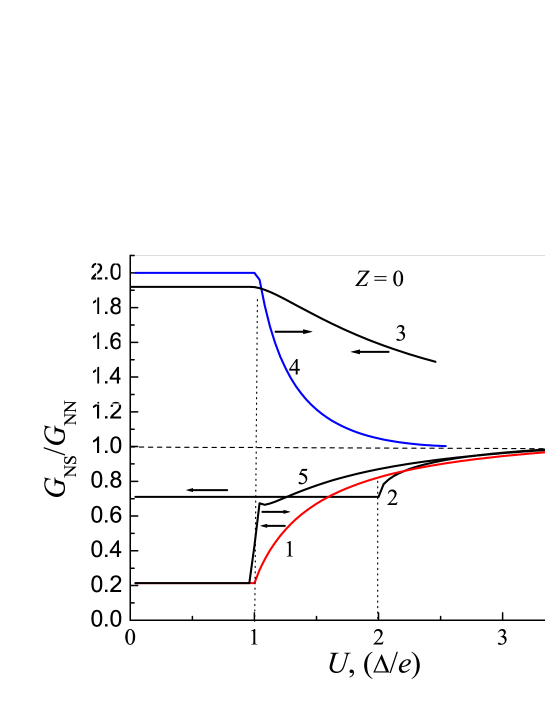
It follows that at the transition of one of the metals of a bimetallic system from the normal to superconducting state, this quantum effect can be identified by a change (decrease) in the voltage U when measured in constant-current regime, or by a change (increase) in the current I in constant-voltage regime, if the system has conductance of a finite value. In the limit of NS bisystem consisting of nondissipative metals with the mean free path of electrons (the BTK model [3]), the role of this conductance will be played by the only conductance in the system - that of the interface, . It will, therefore, concentrate all the voltage U applied to the system, so that (such a quantity we call the generalized conductance, in contrast to the differential one, ). In this limiting case, the role of Andreev reflection is reduced to a twofold change in at the transitions of the system. At energies (T is the temperature), such change will manifest itself in the form of a maximum in conductance curves (see curve 3 in Fig. 1) if there are no additional sources of scattering at the interface (ie, in case of barrier-free interface, , in the terminology of Ref. [3]). Note that in the ballistic approximation, , the generalized and differential conductances of a barrier-free interface are qualitatively of the same shape (compare curves 3 and 4 in Fig. 1).
In the ballistic transport regime, another form of curves is also possible when , namely, the shape of the curve with a dip corresponding to a decrease in the interface conductance with decreasing the transparency of the interface due to existence of a barrier of finite height, , which reduces the probability of Andreev reflection. Thus, in the ballistic transport model, the only possible shapes of the normalized curves (here, is the generalized conductance in the NN state of the system) in the energy range , similar to the form of curves in the same interval, are those with a maximum () or with a dip () [3].
However, as will be seen later, the aforementioned shape of the curves with a dip is not a prerogative of the ballistic model, as is often assumed. The observation of curves of the similar shape in special circumstances, which do not produce any justification for using ballistic conception, indicates the same. The measurement of current-voltage characteristics of the samples with a point-contact geometry (point contacts) must be considered as such special conditions. With high probability we can assume that in the majority of point contacts, prepared in different ways, the ballistic transport conditions are not realized. In this connection, the real curves of point-contact normalized conductance, although visually resembling the curves for the interface conductance in the ballistic model, can have completely different nature and lead to conclusions radically different from those based on the ballistic analysis.
2 Non-ballistic NS point contact
The identification of the experimental curves with the curves of the same shape in the ballistic NS model means automatically that the voltage measured across a real contact is taken entirely related to the NS interface and the interface is considered the only possible source of resistance in the system. In the absence of scattering centers for electrons, the resistance of the interface, , is non-zero due to the effect of "bottleneck" for incompressible media, thus depending only on the cross section of the interface (here, d is the transverse size of the interface). Yu Sharvin was the first to attract attention to this fact [4]:
| (1) |
Here, are the charge, the Fermi momentum and velocity, the concentration and density of states of free electrons per spin, respectively.
For N metals Cu, Al, Au, and Ag commonly used in the contacts we have
| (2) |
if is expressed in cm2. Eq. (2) is a criterion for using ballistic approximation while considering a mode of transport in real point contacts.
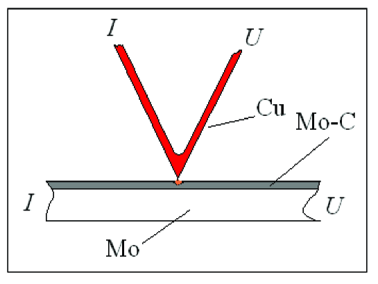
As noted above, both geometrical and physical conditions of measurement of the contact conductance in real experiments cannot meet those of ballistic transport regime. Indeed, a typical longitudinal size of the contacts, , defined by the distance between measuring (potential) probes, is of the order of m or more. This is due to the fact that the geometry of point contacts does not allow one to measure the interface region by a standard four-probe technique, since it appears to be either three-contact, including significant resistance of a probe (usually), or practically two-contact, as is shown in Fig. 2. Because of this, the potential lines, which determine the voltage measured across the probes, in fact, are always on both sides of the interface. They are moved into the depth of both N and S layers at distances comparable to or larger than . As a result, the actual size of the contact is at least an order of magnitude greater than the thickness of the interface (for example, the thickness of oxide layers, Å [5]).
In addition, noting that
| (3) |
( is the resistivity), we find that the condition , under which we cannot assume that the voltage is applied only to the interface, is achieved at for any area of the interface, as this area and N - side cross section are the same, at least within the limits of the distance from the interface of the order of . Hence, an important conclusion follows: The value of the contact resistance which, on the contrary, depends on the cross section, cannot be a criterion for the ballistic nature of transport in the contact.
We illustrate this with two examples. Typical magnitude of the resistivity of copper or gold wires, mm in diameter, which are mostly used as N - side material (probe) in NS contacts, at helium temperatures amounts to , which value, according to Eqs. (2) and (3), should correspond to the mean free path m. This is no less than an order of magnitude shorter than the above estimated , that is inconsistent with the ballistic consideration. At the same time, when the contact area is equal to the cross section of the wire of the specified diameter, the measurement will show the total contact resistance of order of Ohm.
On the contrary, when using the N probe with a working tip size Å, which value is much less than mm ( is the mean free path in the absence of size effect), is approximately equal to and [6]. In this case, the condition which reflects the transition from ballistic to diffusive transport will be satisfied in contacts with the resistances of the order of 10 Ohm or greater at the same liquid-helium temperatures. Clearly, in high-resistance contacts with the resistance of about 100 Ohm it is unacceptable to estimate the interface area (or the size of the probe tip) in accordance with Eq. (3), as is often done, since, under , Eq. (3) underestimates the size of contact area by a factor of (by several orders of magnitude), thereby creating the illusion of ballistic transport. Thus, the condition , inconsistent with the ballistic approximation, appears to be satisfied in most real point contacts regardless of their total resistance. This means that in real contacts, potential bias is distributed along the whole length of the contact rather than concentrating at the interface, as required by the ballistic model.
Consider the metal contact in the absence of oxide layers and additional scattering potentials at the interface (z = 0). In accordance with the additivity rule of resistances (Matthiessen’s rule), generalized contact conductance can be expressed as where is the conductance of the normal region before the interface with cross section and is the conductance of the barrier-free interface. We write the expressions for the current on the N side in the NN and NS states of the interface. Since, as noted above, , then actually coincides with the length of the normal part of the contact, , and in the NN flowing regime the current can be written as
| (4) |
where in addition to Eqs. (1) and (3) we used and .
Similarly, in the NS transport mode ( is the critical temperature of the contact S - side), the current is determined from the condition
| (5) |
Here, the actual interface conductance calculated by the BTK method [3], which takes into account the jump of the distribution function at the interface and the probability of Andreev reflection, can be expressed as follows:
| (6) |
where
Here, are the distribution functions at S and N boundaries of the interface, respectively; ; are the probabilities of Andreev reflection and transitions without and with changing the sign of the wave vectors of electron states, respectively; is the potential jump at the NS boundary that defines the jump of the distribution function. Taking into account that , where is the mean free path of electrons in a dissipative normal region, which may depend on the probability of Andreev reflection (see below), we get Eq. (5) in its final form
| (7) |
An important conclusion follows from this expression for the current in a non-ballistic NS contact: The value of the bias voltage U, at which the transition between the regimes should be observed at a given temperature , must be times higher than the voltage at the interface corresponding to the superconducting gap energy of the S side of the contact. Apparently, this is observed in the majority of point-contact current-voltage characteristics (see, eg, Refs. [7 - 9]). Dividing Eq. (7) by Eq. (4) we obtain an expression for the normalized conductance of a non-ballistic NS hybrid system with an ideal (z=0) interface:
| (8) |
At helium temperatures, under conditions of dominating elastic scattering of electrons by impurities, the N part of the system is a region of coherent scattering of electrons within a distance m from the NS interface. Hence, . Under these conditions, the elastic scattering at the same impurity of the electron and coherently conjugated Andreev hole leads to a twofold increase in the effective scattering cross section, , at that impurity [10], in particular, to a double decrease in the conductance of the next-to-interface N layer as a whole, in thickness [11 - 13]. Accordingly, the dependence of mean free path of electrons on the N side of the NS interface on the probability of Andreev reflection can be expressed as follows [10]:
( in order of magnitude [11]). With this in mind, we note the main features of the curves for non-ballistic contacts with barrier-free () interface in the range of bias voltages . In these circumstances, and
| (9) |
Comparison of the terms in square brackets shows that at z = 0, in the range of values of the bias voltage, when the probability of Andreev reflection is equal to 1, twofold increase in the resistance of non-ballistic contacts due to an increase in the scattering cross section of coherent quasiparticles by impurities dominates over twofold decrease in the intrinsic resistive contribution from the interface (). In particular, in the limit , we get .
Fig. 1 shows generalized normalized conductance of a non-ballistic metallic NS point contact with a barrier-free interface (z = 0) as a function of bias voltage at the contact. The dependencies were calculated numerically by Eq. (8) for two values of the ratio , 1 (curve 1) and 2 (curve 2), in the approximation . Also shown are the same conductance obtained by calculation in the ballistic approximation (curve 3) and the corresponding differential conductance (curve 4). When calculating Eq. (8), the function which depends on the ratio of coherent factors from the Bogolyubov equations, was taken from Ref. [3].
Comparison of the curves 1 - 3 presented in the Figure for the generalized normalized conductance shows at least two major differences between ballistic (curve 3) and non-ballistic (curves 1, 2) contacts. First, the value of at which the behavior of non-ballistic conductance at the NN NS transitions of the system changes radically, depends on the ratio . Second, the asymptotics of are of the opposite nature, both in and in regions. Usually, they analyze the differential conductance, as more expressive, rather than the generalized one. In Fig. 1, curve 5, we show the behavior of the normalized differential conductance of the non-ballistic contact
| (10) |
for the same ratio that corresponds to the generalized conductance depicted by curve 1. It is seen that the main features of the asymptotic behavior in both cases are common.
Thus, the asymptotic behavior of the conductance of non-ballistic contacts appears formally similar to the behavior of of a ballistic contact with the barriers at the interface (see Ref. [3]), which fact is apparently the reason for the application of a ballistic model (often unjustified) while analyzing the curves . Since in this case details of the curves assume a meaning which does not correspond to reality, it can easily lead to wrong conclusions.
Special note is expedient to make in regard to non-ballistic tunnel junctions of hold-down type, with the oxide interface undestroyed, which have semiconductor conductivity as a rule. The resistance of these interfaces can be the greatest in the contact, even in the NN state. In this case, in this state, all the bias voltage will drop at the interface, as a ballistic model assumes. However, since the thickness of the oxide layers t is so small that (see above), then, at the transition from the NN to NS state, due to the proximity effect, the resistance of the oxide layer vanishes, having experienced the superconducting transition in the parameter eU. As a result, a part of the curve of the generalized conductance in some interval of at first takes the shape similar to that of the curves 3 or 4 in Fig. 1. However, at , the potentials will be redistributed, thus transforming transport to the regime where the conductance behaves in accordance with Eq. (8). In high-resistance contacts, the scale of this part of the curve is usually small against that part of the incomparably larger scale, which is associated with the manifestation of the above proximity effect, so that the overall shape of the curve may easily be taken for a behavior of the ballistic conductance to which it has nothing to do.
In this paper, we investigate the behavior of the conductance of non-ballistic point-contact hybrid NS systems with unconventional superconductors, Cu (N) / molybdenum carbide Mo-C (S) and Cu (N) / oxypnictide La[O1-xFx]FeAs (S), , in the Andreev reflection mode.
3 Experiment
25 hybrid contacts have been studied. In Fig. 2, the location of the probes for measuring the characteristics of contacts, including current-voltage ones, is shown. All measurements were performed at a constant dc current. It means that the internal resistance of the current source (this includes regulating resistances) was always greater than the resistance of the contacts. We specifically stipulate that as, while studying high-resistance tunnel NS contacts with semiconducting properties (eg, about 100 Ohm and above), at NN NS transitions, in addition to those features mentioned earlier, the probability of switching preset regimes is not excluded yet, when using a current source with rather low resistance. This can also distort the meaning of the results obtained.
Contacts were made in two ways - by the spark erosion method and mechanically. Contacts made by the first method (Cu/molybdenum carbide Mo-C) have low resistance since the tip touches directly with the superconductor burning the oxide barrier; besides, the area of melted tip in this case was considerable. Contacts made by the second method (Cu/Mo-C and Cu/La[O1-xFx]FeAs) have higher resistance due to conservation of the oxide layer. The difference in resistance between low-resistivity contacts and high-resistivity ones were within two - five orders of magnitude (from Ohm to 1 Ohm). The curves for low-resistance contacts were studied using a piсovoltmeter [14], for high-resistance ones - with the help of a standard measuring technique. Since superconducting carbide layer in Cu/Mo-C samples could be completely destroyed at the point of contact during preparing them by the spark erosion method, we tested the possibility of maintenance of the NS regime in the process of measuring IVC by controlling the type of the temperature dependence of the contact resistance. In this study, we investigated the contacts prepared on the same samples of molybdenum with carbonized surface layer that were described in Ref. [15]. Contacts Cu/La[O1-xFx]FeAs were prepared only by hold-down method. In the NN state, they revealed semiconducting behavior, as well as hold-down contacts Cu/Mo-C.
NS contacts Cu (N) / Mo-C (S)
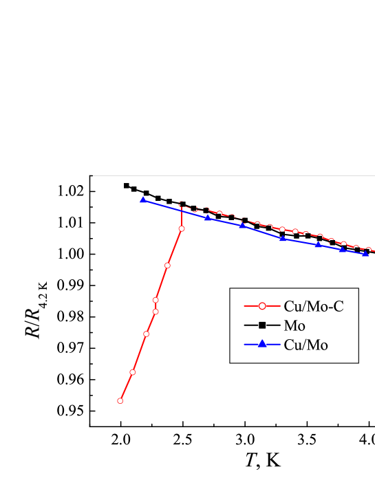
Typical temperature dependencies of the normalized resistance are shown in Fig. 3 for the contact with an undefeated layer of superconducting molybdenum carbide at the interface Cu/Mo-C (circles) and for the contact with a destroyed superconducting layer, ie, Cu/Mo (triangles). Squares depict the resistance of non-carbonized parts of molybdenum measured by a standard four-probe technique. The measured resistance values were normalized to the corresponding contact resistance at 4.2 K. In particular, for a low-resistance contact (the curve with circles), it amounts to Ohm. The dependence of resistance on temperature of this kind, which contains a singularity of the superconducting transition type, indicated the possibility of realizing the transitions NN NS at the contact interface by changing the bias voltage U to a value corresponding to an electron energy of the order of . In our samples of molybdenum carbide, is approximately 2.7 K [15].
Only the conductance of the contacts which revealed such temperature dependence showed features associated with the above transitions in the parameter . Thus, at the transition to the Andreev reflection regime (NN NS), when , the conductance of such contacts always reduced rather than increased, as it could be in the ballistic regime of current flow (see Fig. 1).
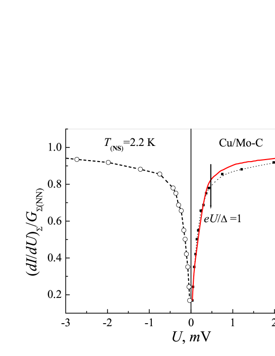
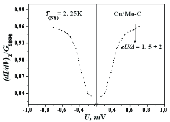
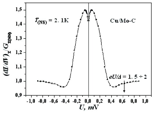
In Figs. 4 and 5, the examples are shown of the behavior of the derivatives of generalized conductance of the investigated contacts with a burned oxide layer, but an undestroyed superconducting carbide Mo-C layer, in the range of bias voltage values of the order of mV. Based on the analysis from the previous section, one can assume that the measured curves describe the behavior of the conductance of a non-ballistic contact with a ratio of about 1 (Fig. 4) or slightly higher (Fig. 5). When the diameter of the interface (probe tip diameter) is about 10 m, an estimation gives the values of the mean free path of electrons in the normal contact area and the size of that area of the order of 0.1 m.
Figure 6 for a contact Cu/Mo-C and Figure 7 for contacts Cu/La[O1-xFx]FeAs can serve as an illustration of the remark made in the previous section concerning the influence of the proximity effect on the shape of the conductance curves for high-resistance hold-down contacts with an undestroyed oxide interface. (We will discuss the latter Figure in more detail below.) In these (always high-resistive) contacts, resistance ratio K) exceeds 1 which fact indicates the presence of an oxide layer with non-metallic conductivity at the interface. If , the contribution from this layer to the contact resistance due to the proximity effect should be absent, as noted earlier, until the electron energy is less than . In this energy range, the probability of Andreev reflection is close to unity and its contribution to the contact resistance is maximum (see a minimum in the curves near in Figs. 6 and 7), since in that range, the mechanism of doubling cross section for scattering of coherent quasiparticles by impurities is responsible for the decrease in conductance. As the energy increases, this resistive contribution, according to Eqs. (9) or (10) (see curves 1 and 5 in Fig. 1), will continue to decrease (increasing conductance) until the order parameter at the interface is suppressed (suppressed proximity effect) and the contribution from a resistive oxide layer becomes to appear, up to the full suppression at . Note that an indistinguishable contribution from the boundary resistance on the S side of the contact is not excluded; that contribution is associated with the charge unbalance of the quasiparticles due to the dispersion of the order parameter at the NS interface, which behaves similarly [16]. In Fig. 6, corresponded to this are those branches of the conductance curve that fall to a value close to unity, with increasing .
In general, one could conclude that the size of non-ballistic contacts with the resistance of no more than 1 Ohm, prepared according to techniques used by us, is of the order of 0.1 m for . There exist non-ballistic contacts with higher resistance, apparently for [7 - 9].
NS contacts Cu (N)/ La[O0.85F≈0.1]FeAs (S)
The emergence of new iron-based superconductors - oxypnictides - caused another burst of interest in the problem of compatibility between superconductivity and magnetism. Experimental investigations of the conductance of point-contact NS heterosystems, with oxypnictides as a superconductor, under conditions of Andreev reflection, seem to be an important trend in the study of this problem. The Andreev reflection is known to lead, in the absence of magnetic fields, to initiation of coherent quasiparticles, e and h, on N side which are related through that reflection at the NS interface. Their coherent scattering by impurities leads, as noted, to a significant decrease in the conductance of non-ballistic NS systems due to doubling scattering cross section. Thus, the behavior of the conductance of NS systems, in particular, with changing the electron energy eU, allows one, above all, to ascertain whether the conductance of the system is of Andreev type and, therefore, to understand, whether the intrinsic magnetism of oxypnictides plays any role in the manifestation of the effects associated with the superconducting properties.
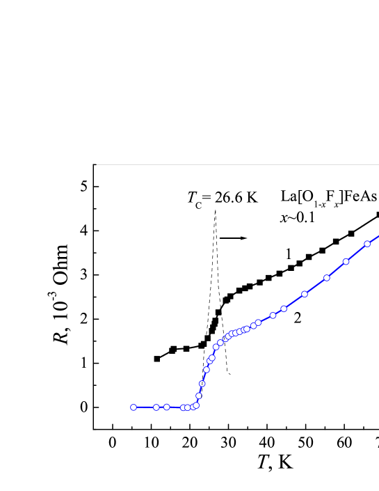
Figure 7 confirms the existence of the superconducting transition in the temperature dependence of resistance of two oxypnictide samples we used to prepare NS point contacts, the conductance of which was then investigated in the regime of Andreev reflection at . Temperature dependence of the resistance of one of the samples was measured by two-probe technique (curve 1) and of the second (curve 2) - by four-probe technique. Indeed, a superconducting feature occurred in the curves R(T) at 26.6 K, as was also observed for oxypnictides La[O1-xFx]FeAs with [1]. We prepared point contacts on these samples by exerting pressure without puncturing the oxide layer, as evidenced by a significant contact resistance under normal current flow (about 10 Ohm at ) and the ratio .

Typical behavior of the conductance of such contacts as a function of bias voltage across the contact is shown in Fig. 8 over a wide range of magnetic fields, B. We see that the feature that can be called a "gap feature" is observed only in the conductance curve measured in the absence of an external magnetic field. This means that the intrinsic magnetism of oxypnictides at does not prevent either the appearance of superconductivity or other effects associated with it, in particular, such as Andreev reflection. This is proved, firstly, by the shape of the feature in the curve for , which just corresponds to a decrease in conductance with decreasing energy , as it should be in the NS regime of non-ballistic contacts when the cross section for the impurity scattering of coherent quasiparticles, coupled by Andreev reflection, is doubled. And, secondly, by the low values of the energy eU compared with , for which the effect exists, that is the values insufficient for suppressing the proximity effect at the interface, and thus, for the manifestation of a non-zero contribution from the boundary resistance, in particular, the resistive contribution from the oxide layer. Since under conditions of non-ballistic transport in the contact, a bias voltage is distributed between the interface and N side of the contact, a position of a gap feature, as shown in Section 2, depends on the ratio (see Fig. 1). From the shape of the curve shown in Fig. 9, which is a part of the curve in Fig. 8 in an enlarged energy scale, it follows that the value of the gap BCS energy of the oxypnictide, mV, at the interface is reached at at the contact. Evaluation by Eqs. (8) and (9) shows that the depth of the minimum in the curve at must be (), which value, as we see, corresponds to the measured one. The normalized conductance curves of point-contact NS systems (including those with an oxypnictide as a superconductor) studied in Ref. [16] can also serve as a good illustration of the discussed features of non-ballistic contact conductance.
The absence of the above effect in external magnetic fields emphasizes, in addition, that this effect is a feature of "Andreev" conductance in conditions of coherence of e and h quasiparticles which takes place only in a zero magnetic field. In a nonzero magnetic field, the coherence of the quasiparticles is disturbed due to spatial divergence of their trajectories after Andreev reflection at NS boundary [18]. As can be seen from Fig. 9, when the bias voltage eU exceeds the energy value , a non-zero "boundary resistance" (the resistance of the oxide layer) appears which was suppressed before by the proximity effect and is influenced by a magnetic field. We omit the detailed discussion of this branch of the curves as not relevant to the merit. However, the impression is that the variation of its shape upon increasing the field is associated with a decrease in carrier mobility in a semiconductor material. The dependence of this part of the contact resistance on the magnetic field is shown in Fig. 10, in which .

Thus, the experiment shows that the presence of a magnetic element in the structure of an oxypnictide has no effect on the manifestation of the phenomenon of Andreev reflection in NS systems with oxypnictides as a superconducting side of the NS interface in the absence of an external magnetic field. In this connection, one can assume that the mechanisms for magnetic interaction, such as ferromagnetic fluctuations, and the mechanism for superconducting pairing of charge carriers (as the results convince, BCS-like) do not overlap in energy in the layered compound La[O1-xFx]FeAs with a 10 % replacement of oxygen by fluorine. It is apparently achieved by a corresponding fragmentation of the Fermi surface of conduction electrons (nesting), which eliminates the competition of these mechanisms at the antiferromagnetic long-range order [19, 20]. The suppression of superconductivity and its attendant effects is observed only in external magnetic fields (in our experiments, at T).

4 Conclusion
In this paper, we consider the behavior of the conductance of point-contact non-ballistic NS heterosystems depending on the electron energy specified by the bias voltage U across the contact. It is noted that curves for non-ballistic and ballistic contacts, having a completely different nature, may, however, coincide in shape, which fact, apparently, is the reason for using, often unjustified, a ballistic model to analyze those curves for real contacts, which are, in fact, non-ballistic. It is shown that the resulting shape of the curves of non-ballistic contacts is determined by the contribution from the mechanism of coherent scattering by impurities. The higher is the probability of Andreev reflection, the greater is that contribution, the greatest at the zero-height barrier at the interface (). The same shape of the conductance curve can be obtained in the ballistic model by fitting the height of the barrier at the interface, thus, by suppressing accordingly the probability of Andreev reflection. Criteria allowing one to differentiate between the regimes of ballistic and non-ballistic transport are given, at apparent similarity of the corresponding conductance curves. One of the major indications of the non-ballistic nature of transport in a contact is the excess of the bias voltage, applied to the contact, above the voltage corresponding to the energy gap of the used superconductor at which NN NS transition is realized. It manifests itself in the form of peculiarities (kinks) in the conductance curves . The analysis is extended to the case of non-ballistic transport in NS point contacts with exotic superconductors, namely, molybdenum carbide, Mo-C, and iron-based oxypnictide, La[O1-xFx]FeAs. The experiment shows that the conductance behavior of the real point contacts of any nature is almost always match that expected for non-ballistic transport regime.
References
- [1] Y. Kamihara, H. Hiramatsu, M. Hirano, R. Kawamura, H. Yanagi, T. Kamiya, and H. Hosono, J. Am. Chem. Soc. 128, 10012 (2006).
- [2] A.F. Andreev, Sov. Phys. JETP 19, 1228 (1964); Sov. Phys. JETP 22, 455 (1966).
- [3] G.E. Blonder, M. Tinkham, and T. M. Klapwijk, Phys. Rev. B 25, 4515 (1982).
- [4] Yu.V. Sharvin, Sov. Phys. JETP 21, 655 (1965).
- [5] P.G. De Gennes, Superconductivity of Metals and Alloys (W.A. Benjamin, New York - Amsterdam, 1966).
- [6] J.M. Ziman, Electrons and Phonons (Clarendon Press, Oxford, 1960).
- [7] R.C. Dynes, V. Narayanamurti, and J.P. Garno, Phys. Rev. Lett. 41, 1509 (1978).
- [8] H. Srikanth and A.K. Raychaudhuri, Physica C 190, 229 (1992).
- [9] A. Plecenik, M. Grajcar, S. Benacka, P. Seidel, and A. Pfuch, Phys. Rev. B 49, 10016 (1994).
- [10] J. Herath and D. Rainer, Physica C 161, 209 (1989).
- [11] A.M. Kadigrobov, Low Temp. Phys. 19, 671 (1993)].
- [12] A. Kadigrobov, L.Y. Gorelik, R.I. Shekhter, et al., Phys.Rev. B 60, 14589 (1999).
- [13] Yu.N. Chiang (Tszyan), in Superconductivity. Theory and Applications, ed. by A.M. Luis (InTech, Croatia, 2011), ch. VI, pp. 99-128.
- [14] Yu.N. Chiang (Tszyan), Prib. Tekhn. Eksp., No. 1, 202 (1985).
- [15] M.O. Dzyuba, Yu.N. Chiang, O.G. Shevchenko, A.V. Semenov, and V.Ph. Khirnyi, Low Temp. Phys. 36, 1036 (2010).
- [16] J. Clarke, U. Eckern, A. Schmid, G. Schön, and M. Tinkham, Phys. Rev. B 20, 3933 (1979); T.Y. Hsiang and J. Clarke, Phys. Rev. B 21, 945 (1980).
- [17] T.Y. Chen, Z. Tesanovic, R.H. Liu, X.H. Chen, and C.L. Chien, Nature 453, 1224 (2008).
- [18] Yu.N. Chiang and O.G. Shevchenko, Low Temp. Phys. 33, 1033 (2007).
- [19] I.I. Mazin, D.J. Singh, M.D. Johannes, and M.H. Du, Phys. Rev. Lett. 101, 057003 (2008).
- [20] Clarina de la Cruz, Q. Huang, J.W. Lynn, Jiying Li, W. Ratcliff II, J.L. Zarestky, H.A. Mook, G.F. Chen, J.L. Luo, N.L. Wang, and Pengcheng Dai1, Nature 443, 899 (2008).