Is adhesion superficial? Silicon wafers as a model system to study van der Waals interactions
Abstract
Adhesion is a key issue for researchers of various fields, it is therefore of uppermost importance to understand the parameters that are involved. Commonly, only surface parameters are employed to determine the adhesive forces between materials. Yet, van der Waals forces act not only between atoms in the vicinity of the surface, but also between atoms in the bulk material. In this review, we describe the principles of van der Waals interactions and outline experimental and theoretical studies investigating the influence of the subsurface material on adhesion. In addition, we present a collection of data indicating that silicon wafers with native oxide layers are a good model substrate to study van der Waals interactions with coated materials.
Saarland University] Department of Experimental Physics, Saarland University, Saarbrücken, 66041, Germany
1 Introduction
Stimulating or preventing adhesion is a key issue for researchers of various fields. To solve these problems, a comprehensive understanding of the prevailing adhesion mechanism is indispensable. Yet, not only various adhesions mechanisms exist, but also plenty of parameters that can affect adhesion: Nanoscale or microscale roughness 1, 2, static charges or the zeta-potential at the interface 3, 4, surface energies 5, 6, and contact shapes 7 are a few frequently-studied examples. All these parameters, however, have in common that they are describing the surface of a material. Hence, the question arises whether adhesion is really only ’superficial‘. This question is of great importance since commonly used photoresists, coatings, adhesion promoters or other functionalized surface layers are often in the range of just a few nanometers. These dimensions are smaller than the range of interactions such as van der Waals (vdW) interactions. Hence, the material right underneath the surface might indeed have an effect on adhesion mediated by vdW interactions. In this paper, we review experimental and theoretical studies investigating the influence of subsurface material on vdW forces. Additionally, we provide a collection of experimental data highlighting the suitability of stratified substrates based on silicon wafers to study vdW interactions.
2 Van der Waals interactions
Already more than hundred years ago van der Waals introduced his theory of an attraction between neutral atoms in order to explain non-ideal gases 9. Later, three types of interactions were identified to contribute to the vdW interactions:
- Keesom interactions
-
characterize dipol-dipol interactions of molecules that carry permanent dipoles 8.
- Debye interactions
-
describe forces between a permanent dipole that induces a dipole moment in an otherwise unpolar molecule 8.
- London interactions,
-
also called dispersion interactions, describe forces between instantaneously induced dipoles 10.
All three parts have in common that the interaction energy scales with . Hence, the vdW potentials for the interactions between two single atoms separated by a distance can be written as
| (1) |
Due to this scaling, vdW interactions are often considered as of short-range.
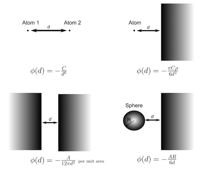
Hamaker, however, calculated energy-distance relations for macroscopic objects by pairwise summation over all atoms, continuing the work of Bradley and DeBoer 11, 12, 13. Depending on the geometry, different scaling laws apply (cf. Figure \plainrefFig:VDWEquations). To account for the properties of the involved materials, Hamaker introduced a coefficient , also called ’Hamaker constant‘, which he defined to
| (2) |
where are the number of atoms per unit volume of the two materials. The controversial subject of Hamaker’s theory was that he assumes a pairwise additivity of the vdW interactions, which is generally speaking not valid. A few years later, Casimir used a completely different ansatz to calculate the force between two ideally conducting semi-infinite half-spaces in vacuum 14. On the basis of Planck’s famous theory, he summed up the allowed electromagnetic modes between two conducting plates. Lifshitz extended Casimir’s idea and presented a theory for arbitrary materials, based on quantum field theory 15. In principle, although many studies differentiate between Lifshitz-vdW and Casimir interactions, Lifshitz and Casimir essentially described the same effect, but with different foci 16, 17. By treating the interacting objects as continuous media, Casimir’s and Lifshitz’ theories circumvent the question of pairwise additivity. Interestingly, Lifshitz’ ansatz led to the same scaling laws as the classical Hamaker ansatz (cf. Figure \plainrefFig:VDWEquations). Only the way the Hamaker constants are derived is different. Following Lifshitz’ theory, they are calculated from the optical properties of the involved materials and can be approximated (see Appendix) by
| (3) |
with the dielectric constants , the refractive indices in the visible regime , and the main electronic absorption frequency .
The works of Hamaker, Casimir and Lifshitz demonstrate that vdW-Casimir interactions can indeed be regarded as of long-range, since for mesoscopic and macroscopic objects, the absolute value of the exponent of the scaling law is decreased (the interaction between two semi-infinite half slabs scales with , for instance). Yet, the long-range character is restricted due to the finite speed of light 18. This retardation effect increases the absolute value of the exponent of the scaling law by up to one (for nm). For separations smaller than 10 nm, however, the retardation can usually be neglected 19, 20.
3 Van der Waals interactions with coated substrates
Using the equations given by the theories mentioned above, it is usually possible to predict the potentials for the interactions of two uniform objects. Yet, many systems consist of coated substrates. However, VdW interactions act not only between atoms in the vicinity of the surface, but also between atoms in the bulk material. Early experiments of Israelachvili und Tabor, showed that in the case of mica substrates covered with a monomolecular layer of stearic acids, both the acids and the mica contribute to the vdW interactions 21. These experimental studies were in agreement with theoretical predictions of Langbein, who postulated that the interactions with the surface layer dominate for separations smaller than the layer thickness () and the interactions with the bulk material dominate in the opposing limit () 22, 23. More recent studies showed that variations in the thickness of a surface layer induce differences in the vdW potentials and influence e.g. the stability of thin liquid coatings 24, 25, 26, 27. These thin film dewetting studies moreover demonstrated quantitatively the impact of the subsurface composition to the effective interface potential 28: The impact was measured experimentally by determining the differences in the preferred wavelength of spinodally dewetting thin films with variable subsurface composition 24, 29.
3.1 Interactions in biological systems
VdW interactions also play a major role in biological systems 30. Particularly non specific adhesion is governed by vdW interactions in conjunction with electric double layer interactions, usually described using the DLVO-theory 3, 31 or extended DLVO-theory 32. Many biological processes, such as the aggregation of proteins 33, the unspecific adhesion of cells and bacteria 34, 35, 36, the adherence of abalones 37, and the sticking of geckos 38, 39, 40 are influenced and sometimes dominated by vdW interactions. As a logical consequence, these processes are also not ‘purely superficial’, viz. not solely dependent on the properties of the surface. It could be shown that, when interacting with a coated substrate, proteins indeed sense both, the surface layer and the underlying material: Adsorption experiments on tailored silicon wafers with differences in the thickness of the oxide layer on top of the wafers revealed qualitatively different adsorption kinetics of multiple types of proteins 41, 42. Based on Monte-Carlo simulations featuring surface processes such as surface mobility and conformational changes, the distinctions were invoked by the influence of the vdW-interactions on the time scale of these processes 43. X-ray reflectivity experiments corroborated these findings 44. Recent studies discovered that the influence of the subsurface material on adhesion is sensed by larger biological objects, too: The unspecific adhesion of bacteria from the Staphylococcus genus is affected by the properties of the subsurface material, as could be shown by AFM force spectroscopy measurements 45. Moreover, adhesion experiments with setal arrays of live geckos revealed that the adhesion force was significantly varied by a change in the substrates subsurface composition 46.
3.2 Theoretical description of multilayer systems
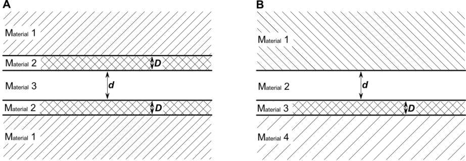
For a comprehensive theoretical description of the vdW potentials for systems involving multilayer structures, not only the surface layer, but also the composition of the entire substrate has to be taken into account. Unfortunately, there is no general equation for the vdW interactions between arbitrary objects and layered substrates. In the following we therefore will focus on the non-retarded interactions between infinite planar interfaces.
Generally, a common way to find out unknown Hamaker constants is the use of combining rules (geometric mean) 47. These relations, that are derived from the combining rules for surface energies, may be used to calculate ‘effective’ Hamaker constants for a multilayer system. Yet, these relations break down whenever the Keesom and Debye part (the zero frequency terms) cannot be neglected 8. Especially in multilayer systems, where multiple Hamaker constants are necessary, combining rules are not applicable. On the basis of the Lifshitz theory, the potentials for the interactions of symmetrical triple layer films (cf. Figure \plainrefFig:LayerSystem A) were calculated by
| (4) |
with the constants for the interactions of the two different interfaces 48, 49, 50. Using the same ansatz, the vdW potential of the interactions between a probe material and a substrate coated with a layer of thickness (cf. Figure \plainrefFig:LayerSystem B) is given by 49, 17
| (5) |
For larger separations , however, Eq. (\plainrefEq:CoatedLayer) is no longer valid. For the description of an experimental system with a variable (e.g. a thickness of a coating), we have previously chosen an alternative approximation 24, 26: By assuming a scaling of the interaction with and a continuous transition between the boundary cases and , we gained
| (6) |
where stands for the interaction of material 1 via medium 2 with material 4 in the case that , viz. medium 3 is nonexistent.
4 Silicon wafers as a model system
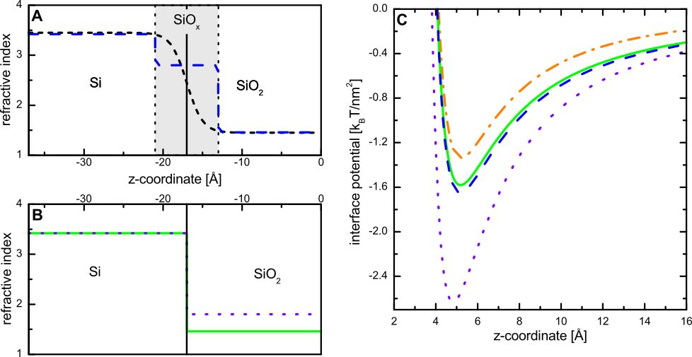
Most of the studies mentioned above used silicon wafers as a model system to study vdW interactions with coated materials. As described earlier, these interactions are essentially dependent on the optical properties of the involved materials (Eq. (\plainrefEq:HamakerIsra)). The properties of silicon oxide films, however, have been discussed controversially for decades. In the following, the term “silicon oxide” stands for SiOx. The use of SiO2 bulk values for oxide films thicker than 100 nm is generally accepted. Yet, the validity of these values for thin film has been questioned numerous times and especially the optical properties, such as the refractive index, are disputed. In general, thin silicon oxide layers may be described by two different models:
- Single layer model:
-
By assuming a sharp transition between the bulk Si and the oxide, the latter can be described by a single layer (cf. Figure \plainrefFig:ThinSiOFilms A). In this case, the oxide layer may have the same refractive index as bulk SiO2 or an increased refractive index.
- Double layer model:
-
Since a sharp transition between the materials is highly unphysical, a continuous transition or an interface roughness is very likely. As the thickness of this transition region is of the same order of magnitude as the oxide layer thickness, a double layer configuration is a obvious approximation (cf. Figure \plainrefFig:ThinSiOFilms B).
The van der Waals interactions sensed by an probe object should differ strongly for these different model configurations (cf.Figure \plainrefFig:ThinSiOFilms C).
| oxide layer | [nm] | [nm] | [∘] | [∘] | [mJ/m2] |
|---|---|---|---|---|---|
| native | 1.7(3) | 0.13(3) | 5(2) | compl. wetting | 63(1) |
| thick | 150(1) | 0.09(2) | 7(2) | compl. wetting | 64(1) |
By applying the single layer model\bibnoteJellison indeed assumed a transition layer. Yet, at some point (for thin films) he started to neglect this layer, whereby the increase in refractive index began exactly around this point., Jellison observed an increase in the refractive index of the whole oxide layer 54. Using spectroscopic polarization modulation ellipsometry, the refractive index of very thin layers was determined to (at nm). These findings were later on confirmed by other studies 55, 56.
Experimental support for the double layer model, viz. the observation of an interfacial transition layer, is also given by previous studies. Experimental studies noticed a thin ( Å) region of atomically mixed Si and O with an refractive index of (at 546.1 nm) 57, 58. High-resolution core-level and XPS spectroscopy 59, 60 also confirmed that “the interface is not abrupt, as evidenced by the high density of intermediate-oxidation states (about two monolayers of Si) and by their nonideal distribution” 61. These findings were matched by predictions of theoretical models 62, 63.
The results of theses studies, however, are not contradictory, but arise from the different methods applied. A problem of optical reflectivity methods, such as ellipsometry, is that they are not able to determine the density and the thickness of thin films (nm) independently (not to mention to distinguish between two of such films). Thus, the usage of the single layer model for these methods is the only possible way. Yet, for thinner silicon oxide films, the transition layer fraction of the total oxide layer is increased resulting in an observation of a higher overall refractive index.
Another limitation of all of the mentioned studies is, that they are performed on silicon wafers with thermally grown silicon oxide layers. Especially for thin ( nm) films, the process parameters of the artificial growing process can have a significant influence on the density and the optical properties of the silicon oxide (decreased vs. increased refractive index) 64, 65. Yet, already without any pretreatment, silicon wafers are covered with a native oxide layer of 1.5 nm to 2 nm thickness. Since only limited data is available for the optical properties of native oxide layers, we present a brief summary of the properties of these layers containing previously unpublished data.
4.1 Properties of thin native oxide layers
The increase in refractive index to values up to , as predicted by several studies 54, 55, 56, is highly unlikely for native oxide layers as polymer dewetting studies have shown via an indirect way 24: Thin liquid polystyrene (PS) films prepared on Si wafers with native oxide layers (nm) were unstable and dewetted spinodally. Since this process is driven by the minimization of the free energy determined by the vdW potential 66, 8 the refractive indexes of the oxide cannot be higher than the one of PS (), as shown by Eq. (\plainrefEq:HamakerIsra).
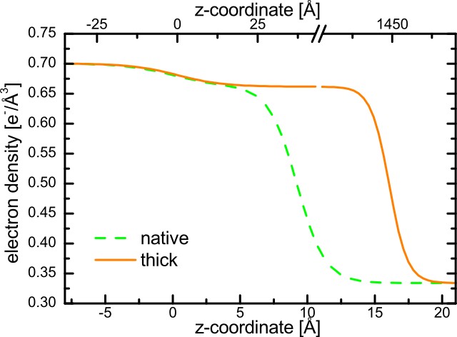
A more direct ansatz is to compare native oxide layers to thick oxide layers in terms of the material properties, such as surface roughness, surface chemistry, homogeneity, electron density and stoichiometry: The surface characterization via atomic force microscopy (AFM) and contact angle (CA) measurements shows that - within the experimental error - the roughness and chemical homogeneity of the surface of a native oxide layer on Si wafers does not differ from the properties of a thick SiO2 layer (cf. Table \plainrefTab:SurfaceProperties). The analysis of high energy X-ray reflectivity measurements on native and thick oxide layers leads to electron densities that are again similar (Figure \plainrefFig:XrayThinSiO). Especially the topmost part ( Å) of the native oxide layer resembles the density of the thicker layer.
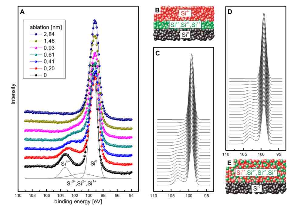
The stoichiometry of the native oxide layer was studied by X-ray photoelectron spectroscopy (XPS) combined with Ar ion etching in order to reveal the depth profiles for different oxidation states/valencies Sik+ (). Figure \plainrefFig:XPSThinSiO A shows the Si-2p spectra recorded in normal emission mode (take-off angle 0∘ along the surface normal) with two components representing Si0 and Si4+ at lower and higher binding energy, respectively. Contributions from Si1+, Si2+ and Si3+ could not be resolved, but have to be treated as a third peak in the background between the Si0 and Si4+ signals. For stepwise ablation of the surface, the intensity of the Si4+ peak decreases asymmetrically, i.e., it is shifted towards the Si0 signal, forming a shoulder in the intermediate state before vanishing (for calibration of ablation see, e.g., Ref. 67). For ablation of about 1.5 nm, contributions from oxide species can no longer be observed, which is in accordance with the thickness of the native oxide measured by other methods (Figure \plainrefFig:XrayThinSiO and Table \plainrefTab:SurfaceProperties). The asymmetry in the Si oxide related part of the spectra is characteristic for intensity contributions from Si4+ and (Si1+, Si2+, Si3+) when distributed in a double layer model as depicted in Figure \plainrefFig:XPSThinSiO B. For this type of stacking, the simulation of intensity distributions within the Si-2p spectra in Figure \plainrefFig:XPSThinSiO C shows the same characteristics, namely the asymmetric decrease of the intensity from the oxide species as the experimental data in Figure \plainrefFig:XPSThinSiO A. A similar asymmetry was reported in previous studies on thermally grown oxide layers 60. For comparison, Figure \plainrefFig:XPSThinSiO E shows a second model with a homogeneous distribution of the oxidation states within the oxide layer. For this scenario, the simulation in Figure \plainrefFig:XPSThinSiO D predicts a uniform disappearance of the oxide contributions, in contrast to the experimental observations in Figure \plainrefFig:XPSThinSiO A.
In summary, these results show that native silicon oxide layers can be approximated by a double layer system as depicted in Figure \plainrefFig:ThinSiOFilms A and Figure \plainrefFig:XPSThinSiO B, where adjacent to the bulk Si a transition layer and then a bulk-like SiO2 layer follows. Since all characterized material properties of the SiO2 part are similar to the properties of thick oxide layers, there are no hints to assume different optical properties. The transition layer, however, will most likely display increased polarizability 57, 58, 63. That means, differences in the vdW potentials wafers featuring native and thick oxide layers arouse indeed from subsurface contributions, since the uppermost material is the same, namely SiO2. Hence, silicon wafers with native oxide layers are indeed a good model substrate to study van der Waals interactions with coated materials.
5 Appendix
5.1 Calculation of Hamaker constants
Based on the Lifshitz theory, the Hamaker constant can be calculated by\bibnoteThe prime denotes that the zero term has to be multiplied with .
| (7) |
with
| (8) |
whereby are the values of the dielectric function of material at the imaginary (Matsubara) frequencies
| (9) |
Using the Ninham-Parsegian approximation it is possible to obtain the from the adsorption spectrum 69, 48, more precisely the relative strengths and the frequencies of the peaks, by
| (10) |
with
| (11) |
where is the strength of an oscillator, its relaxation frequency, and N is the total number of oscillators. For dielectric materials Eq. (\plainrefEq:Epsilon) reduces to 70, 71
| (12) |
with the molecular rotational relaxation frequency (typically in the IR regime), the main electronic absorption frequency (typically s-1, in the UV regime), and the refractive index in the visible regime. As usually (cf. Eq. (\plainrefEq:Matsubara)) the first term in Eq. (\plainrefEq:ReducedDielectric) can be neglected and Eq. (\plainrefEq:HamakerLifshitz) may be approximated by Eq. (\plainrefEq:HamakerIsra) if the adsorption frequencies of the three materials are similar 8.
References
- Fuller and Tabor 1975 Fuller, K. N. G.; Tabor, D. Proc. R. Soc. Lond. A 1975, 345, 327–342
- Persson and Tosatti 2001 Persson, B. N. J.; Tosatti, E. J. Chem. Phys. 2001, 115, 5597–5610
- Derjaguin and Landau 1941 Derjaguin, B. V.; Landau, L. Acta Physicochim. URS 1941, 14, 633–662
- Yoon and Lenhoff 1992 Yoon, B. J.; Lenhoff, A. M. J. Phys. Chem.-Us 1992, 96, 3130–3134
- Johnson et al. 1971 Johnson, K. L.; Kendall, K.; Roberts, A. D. Proc. R. Soc. A 1971, 324, 301–313
- Good 1992 Good, R. J. J. Adhes. Sci. Technol. 1992, 6, 1269–1302
- Spolenak et al. 2005 Spolenak, R.; Gorb, S. N.; Gao, H.; Arzt, E. Proc. R. Soc. A 2005, 461, 305–319
- Israelachvili 1992 Israelachvili, J. N. Intermolecular and Surface Forces, 2nd ed.; Academic Press: San Diego, 1992
- Van der Waals 1873 Van der Waals, J. D. Die Kontinuität des gasformigen und des flüssigen Zustandes. Ph.D. thesis, Leiden, 1873
- London 1937 London, F. T. Faraday Soc 1937, 33, 8–26
- de Boer 1936 de Boer, J. H. T. Faraday Soc. 1936, 32, 10–37
- Bradley 1932 Bradley, R. S. Phil. Mag. 1932, 13, 853–862
- Hamaker 1937 Hamaker, H. C. Physica 1937, 4, 1058–1072
- Casimir 1948 Casimir, H. B. G. Proc. K. Ned. Akad. Wet. 1948, 51, 793
- Dzyaloshinskii et al. 1961 Dzyaloshinskii, I. E.; Lifshitz, E. M.; Pitaevskii, L. P. Adv. Phys. 1961, 10, 165–209
- French et al. 2010 French, R. H. et al. Rev. Mod. Phys. 2010, 82, 1887–1944
- Parsegian 2006 Parsegian, V. A. Van der Waals forces, 1st ed.; a handbook for biologists, chemists, engineers, and physicists; Cambridge University Press: New York, 2006
- Casimir and Polder 1948 Casimir, H. B. G.; Polder, D. Phys. Rev. 1948, 73, 360–372
- Tabor and Winterton 1969 Tabor, D.; Winterton, R. H. S. Proc. Roy. Soc. A. 1969, 312, 435–450
- Israelachvili and Tabor 1972 Israelachvili, J. N.; Tabor, D. Nature 1972, 236, 106
- Israelachvili and Tabor 1972 Israelachvili, J. N.; Tabor, D. Proc. R. Soc. A 1972, 331, 19–38
- Langbein 1971 Langbein, D. J. Phys. Chem. Solids 1971, 32, 1657–1667
- Langbein 1972 Langbein, D. J. Adhes. 1972, 3, 213–235
- Seemann et al. 2001 Seemann, R.; Herminghaus, S.; Jacobs, K. Phys. Rev. Lett. 2001, 86, 5534–5537
- Seemann et al. 2001 Seemann, R.; Herminghaus, S.; Jacobs, K. J. Phys.: Condens. Matter 2001, 13, 4925–4938
- Jacobs et al. 2008 Jacobs, K.; Seemann, R.; Herminghaus, S. In Polymer Thin Films; Tsui, O. K. C., Russel, T. P., Eds.; World Scientific: Singapore, 2008; pp 243–266
- Bäumchen and Jacobs 2010 Bäumchen, O.; Jacobs, K. J. Phys.: Condens. Matter 2010, 22, 033102
- Vrij 1966 Vrij, A. Discuss. Faraday Soc. 1966, 42, 23–33
- Herminghaus et al. 1998 Herminghaus, S.; Jacobs, K.; Mecke, K.; Bischof, J.; Fery, A.; Ibn-Elhaj, M.; Schlagowski, S. Science 1998, 282, 916–919
- Leckband and Israelachvili 2001 Leckband, D.; Israelachvili, J. N. Q. Rev. Biophys. 2001, 34, 105–267
- Verwey and Overbeek 1948 Verwey, E. J. W.; Overbeek, J. T. G. Theory of the Stability of Lyophobic Colloids, 1st ed.; Elsevier Publishing Co: Amsterdam, 1948
- Van Oss 1989 Van Oss, C. J. Cell Biochem. Biophys. 1989, 14, 1–116
- Leckband et al. 1994 Leckband, D.; Schmitt, F.; Israelachvili, J. N.; Knoll, W. Biochemistry-Us 1994, 33, 4611–4624
- Nir and Andersen 1977 Nir, S.; Andersen, M. J. Membrane Biol. 1977, 31, 1–18
- Nir 1977 Nir, S. Prog. Surf. Sci. 1977, 8, 1–58
- Ploux et al. 2010 Ploux, L.; Ponche, A.; Anselme, K. J. Adhes. Sci. Technol. 2010, 24, 2165–2201
- Lin et al. 2009 Lin, A. Y. M.; Brunner, R.; Chen, P. Y.; Talke, F. E.; Meyers, M. A. Acta Mater. 2009, 57, 4178–4185
- Autumn et al. 2002 Autumn, K.; Sitti, M.; Liang, Y. C. A.; Peattie, A. M.; Hansen, W. R.; Sponberg, S.; Kenny, T. W.; Fearing, R. S.; Israelachvili, J. N.; Full, R. J. Proc. Natl. Acad. Sci. 2002, 99, 12252–12256
- Autumn and Peattie 2002 Autumn, K.; Peattie, A. M. Integr. Comp. Biol. 2002, 42, 1081–1090
- Huber et al. 2005 Huber, G.; Mantz, H.; Spolenak, R.; Mecke, K.; Jacobs, K.; Gorb, S. N.; Arzt, E. Proc. Natl. Acad. Sci. 2005, 102, 16293–16296
- Quinn et al. 2008 Quinn, A.; Mantz, H.; Jacobs, K.; Bellion, M.; Santen, L. Europhys. Lett. 2008, 81, 56003
- Schmitt et al. 2010 Schmitt, Y.; Hähl, H.; Gilow, C.; Mantz, H.; Jacobs, K.; Leidinger, O.; Bellion, M.; Santen, L. Biomicrofluidics 2010, 4, 032201
- Bellion et al. 2008 Bellion, M.; Santen, L.; Mantz, H.; Hähl, H.; Quinn, A.; Nagel, A. M.; Gilow, C.; Weitenberg, C.; Schmitt, Y.; Jacobs, K. J. Phys.: Condens. Matter 2008, 20, 404226
- 44 Hähl, H.; Evers, F.; Grandthyll, S.; Paulus, M.; Sternemann, C.; Loskill, P.; Lessel, M.; Hüsecken, A. K.; Brenner, T.; Tolan, M.; Jacobs, K. submitted
- 45 Loskill, P.; Hähl, H.; Kreis, C. T.; Thewes, N.; Bischoff, M.; Herrmann, M.; Jacobs, K. submitted
- 46 Loskill, P.; Puthoff, J. B.; Wilkinson, M.; Mecke, K.; Jacobs, K.; Autumn, K. submitted
- Van Oss and Chaudhury 1988 Van Oss, C. J.; Chaudhury, M. K. Chem Rev 1988, 88, 927–941
- Ninham and Parsegian 1970 Ninham, B. W.; Parsegian, V. A. J. Chem. Phys. 1970, 52, 4578–4587
- Parsegian and Ninham 1973 Parsegian, V. A.; Ninham, B. W. J. Theor. Biol. 1973, 38, 101–109
- Parsegian 1993 Parsegian, V. A. Langmuir 1993, 9, 3625–3628
- Sze and Ng 2006 Sze, S. M.; Ng, K. K. Physics of semiconductor devices, 3rd ed.; John Wiley & Sons: New York, 2006
- Mykhaylyk et al. 2003 Mykhaylyk, T. A.; Evans, S. D.; Fernyhough, C. M.; Hamley, I. W.; Henderson, J. R. J. Colloid. Interface. Sci. 2003, 260, 234–239
- 53 Jellison indeed assumed a transition layer. Yet, at some point (for thin films) he started to neglect this layer, whereby the increase in refractive index began exactly around this point.
- Jellison Jr 1991 Jellison Jr, G. E. J. Appl. Phys. 1991, 69, 7627–7634
- Wang and Irene 2000 Wang, Y.; Irene, E. A. J. Vac. Sci. Technol. B 2000, 18, 279–282
- Hebert et al. 1996 Hebert, K. J.; Zafar, S.; Irene, E. A.; Kuehn, R.; McCarthy, T. E.; Demirlioglu, E. K. Appl. Phys. Lett. 1996, 68, 266–268
- Taft and Cordes 1979 Taft, E.; Cordes, L. J. Electrochem. Soc. 1979, 126, 131–134
- Aspnes and Theeten 1979 Aspnes, D. E.; Theeten, J. B. Phys. Rev. Lett. 1979, 43, 1046–1050
- Hollinger and Himpsel 1984 Hollinger, G.; Himpsel, F. J. Appl. Phys. Lett. 1984, 44, 93–95
- Grunthaner et al. 1979 Grunthaner, F. J.; Grunthaner, P. J.; Vasquez, R. P.; Lewis, B. F.; Maserjian, J.; Madhukar, A. J. Vac. Sci. Technol. 1979, 16, 1443–1453
- Himpsel et al. 1988 Himpsel, F. J.; McFeely, F. R.; Taleb-Ibrahimi, A. Phys. Rev. B: Condens. Matter 1988, 38, 6084–6096
- Ohdomari et al. 1987 Ohdomari, I.; Akatsu, H.; Yamakoshi, Y.; Kishimoto, K. J. Appl. Phys. 1987, 62, 3751–3754
- Giustino et al. 2005 Giustino, F.; Bongiorno, A.; Pasquarello, A. J. Phys.: Condens. Matter 2005, 17, S2065–S2074
- Irene et al. 1982 Irene, E.; Tierney, E.; Angilello, J. J. Electrochem. Soc. 1982, 129, 2594–2597
- Cai et al. 2010 Cai, Q.-Y.; Zheng, Y.-X.; Mao, P.-H.; Zhang, R.-J.; Zhang, D.-X.; Liu, M.-H.; Chen, L.-Y. J. Phys. D: Appl. Phys. 2010, 43, 445302
- Geoghegan and Krausch 2003 Geoghegan, M.; Krausch, G. Prog. Polym. Sci. 2003, 28, 261–302
- Müller et al. 2010 Müller, F.; Zeitz, C.; Mantz, H.; Ehses, K.-H.; Soldera, F.; Schmauch, J.; Hannig, M.; Hüfner, S.; Jacobs, K. Langmuir 2010, 26, 18750–18759
- 68 The prime denotes that the zero term has to be multiplied with .
- Parsegian and Ninham 1969 Parsegian, V. A.; Ninham, B. W. Nature 1969, 224, 1197–1198
- Mahanty and Ninham 1976 Mahanty, J.; Ninham, B. W. Dispersion forces, 1st ed.; Academic Press: London, 1976
- Hough and White 1980 Hough, D. B.; White, L. R. Adv. Colloid Interface Sci. 1980, 14, 3–41