english
Evidence for Charging Effects in CdTe/CdMgTe Quantum Point Contacts
Abstract
Here we report on fabrication and low temperature magnetotransport measurements of quantum point contacts patterned from a novel two-dimensional electron system — CdTe/CdMgTe modulation doped heterostructure. From the temperature and bias dependence we ascribe the reported data to evidence for a weakly bound state which is naturally formed inside a CdTe quantum constriction due to charging effects. We argue that the spontaneous introduction of an open dot is responsible for replacement of flat conductance plateaus by quasi-periodic resonances with amplitude less than , as found in our system. Additionally, below K a pattern of weaker conductance peaks, superimposed upon wider resonances, is also observed.
pacs:
73.63.Rt, 73.23.Ad, 73.20.FzQuantum point contacts (QPCs) are conventionally considered as open mesoscopic systems and their characteristic feature, i.e. integer quantized conductance , is well-understood as a single electron effect van Wees et al. (1991). Nevertheless, some additional non-integer anomalous resonances are also commonly observed at low temperatures and their exact origin is under active debate. Generally they are attributed to electron-electron (e-e) interactions and more specifically, to the formation of quasi-bound states inside the constriction. Such charge droplets may reveal the Kondo physics or become, via the exchange energy term, ferromagnetically polarized *[][; andreferencestherein.]Berggren2010. To date, the physical mechanism of localization is still unclear and the role of charging effects Sablikov et al. (2000) in the spontaneous formation of an open dot remains controversial. Therefore, a semiconducting material with a large ratio of Coulomb to kinetic energies is expedient to resolve those important issues and is potentially useful for spintronic applications.
Motivated by these considerations we report on fabrication and low temperature magnetotransport measurements of quantum point contacts, patterned from n-type CdTe/CdMgTe modulation doped quantum well Piot et al. (2010), not studied before in the ballistic transport regime. It is expected that the correlations effects in CdTe are stronger, as compared to GaAs, since the effective mass is larger and the dielectric constant is smaller. As a result, the average distance between electrons , expressed in effective Bohr radius units, is times larger for CdTe than for GaAs with the same carrier density. In this report we provide the evidence for spontaneous formation of quasi-bound state in short and nominally symmetric QPCs, which suggests that the counter-intuitive appearance of localisation is caused by e-e correlations. This is supported by the temperature and bias dependence of observed conductance resonances.
Four-terminal quantum point contacts have been made of high quality two-dimensional electron gas (2DEG) with concentration and mobility . The nanojunctions of length m and lithographic width m are patterned by e-beam lithography and deep-etching techniques. Carrier density in those devices is controlled by means of V-shaped side gates which are separated from the constriction area by narrow etched grooves, see inset to Fig. 1. A modulation doped quantum well is located nm below the surface of the device and ohmic contacts have been prepared by direct indium soldering. The differential conductance has been measured in He-3 cryostat as a function of dc source-drain bias and in-plane magnetic field by employing a standard low-frequency lock-in technique, with ac excitation voltage of V. Data collected at different cooldowns from room temperature demonstrate similar characteristics.
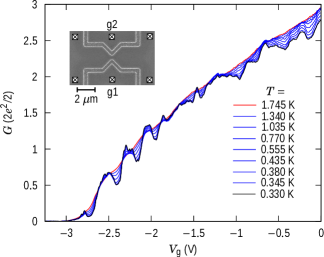
We have studied several devices of the same geometry, however, perfect conductance quantization with plateaus is never observed. The electron mean free path of the 2DEG is m and chemically etched grooves are rather smooth. Also, the estimated physical width of the constriction is much smaller than (see below) and the quantum lifetime ps is rather large Piot et al. (2010), therefore the absence of flat conductance steps is quite unexpected. Figure 1 shows differential conductance data, obtained for the most comprehensively studied QPC sample. is not perfectly quantized vs gate voltage, however, quasi-periodic conductance oscillations with amplitude less than are clearly visible. Additionally, at low temperatures ( K) a weaker pattern of less regular and narrower fluctuations is observed. Some of the random fluctuations are caused by disorder, but regular conductance resonances with amplitude reduced down to must be related to a subsequent population of 1D channels. The energy distance between quantized modes meV has been obtained from the bias dependence, therefore the physical width of our device is estimated as nm for Fermi energy meV (assuming parabolic confinement).
Reduced steps and conductance resonances had been already observed for longer quantum wires or disordered QPCs made of AlGaAs/GaAs heterostructures van Wees et al. (1991); Wróbel et al. (1992). They are commonly attributed to a single electron interference and back-scattering effects caused by disorder. This mechanism is supported by the temperature dependence of conductance traces, recorded vs . At few kelvins, curves are rather smooth and monotonic, whereas at lower fluctuations and resonances show up and regions with positive and negative temperature gradient appear. In an one-electron picture this is explained by thermal averaging which smooths out an interference pattern. At first sight a similar behaviour is observed in Fig. 1, yet a closer look disclose important differences.
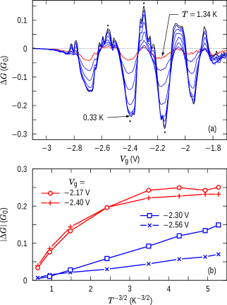
In order to show the temperature dependence of conductance resonances in more detail, values have been calculated by subtracting a smooth curve measured for K from all other data, collected at lower temperatures. Results are summarized in Figure 2. reveals five regular oscillations which are smoothed out when temperature increases, however, quite distinct thermal averaging scenarios are found, according to the sign. Conductance anti-resonances (, with positive temperature dependence, are practically unchanged up to K and then start to disappear. At the same time, resonances ( show stronger, approximately like , low temperature dependence, as demonstrated in Fig. 2(b). Furthermore, up to smaller, quasi-periodic conductance peaks are superimposed on wider oscillations up to . This was not reported in earlier mesoscopic studies of disordered QPCs. The overall picture is therefore more complicated than the one provided by interference of electron waves and suggests a role of the e-e correlations.
Conductance data presented in Figs 1 and 2 demonstrate striking similarities with curves obtained for long ( m) GaAs quantum point contact, with centrally embedded open quantum dot Liang et al. (1998); Tkachenko et al. (2001). For such a specially designed device, conductance oscillations with reduced height (from to , depending on the dot size) were observed in place of a flat plateaus. They were interpreted as a Fabry-Perot like resonances, placed above the threshold of each quantized channel. The amplitude of resonances must be reduced, because potential barriers at the entrance and at the exit to the dot will never be exactly the same Tkachenko et al. (2001). Additionally, the Coulomb charging effects in an open dot manifested itself as a smaller and narrower periodic peaks overlaying upon wider anti-resonances. The amplitude of Coulomb peaks increased monotonically down to K. Clearly, similar features are observed in Fig. 2. Therefore, narrow resonances with temperature dependence may be related to the quantization of charge which gradually fills shallow potential well when gate voltage increases. Recently, residual charge quantization has been directly observed for GaAs open quantum dot by capacitance measurements Amasha et al. (2011).
Self-consistent calculations suggest that quasi-localized states exist also in a large class of smoothly varying constrictions patterned without the intentional central widening. When interactions at wider regions of QPC are taken into account, the narrowest middle part may be spontaneously charged and form an open dot Hirose et al. (2003). This effect is very length dependent — for very short constrictions bound states are not created, whereas for longer devices a chain of charge droplets is predicted to occur Rejec and Meir (2006). If the device is sufficiently long ( nm, for GaAs) quasi-localized states may develop also for higher densities, when more then one channel is occupied Ihnatsenka and Zozoulenko (2007).
Nevertheless, the physical mechanism of electron localization remains unclear and its influence on conductance measurements is highly debated. Recently it has been proposed Song and Ahn (2011) that longitudinal resonant levels are formed within the constriction due to momentum mismatch and interference effects. In contrary, previous literature suggests Shchamkhalova and Sablikov (2007) that the creation of quasi-bound states is caused by Friedel oscillations of electron density which emerge at two opposite sides of the QPC and form potential barriers which surround the central part of a device. A barrier for the open channel arises from the interaction with electrons from all closed channels, which are reflected at side boundaries.
Moreover, if Friedel oscillations (FO) are responsible for barrier formation, the energy averaging must lead to an overall increase in conductance with increased temperature, since then barriers are smoothed. This scenario has recently been supported by numerical simulations and observed experimentally for a clean GaAs quantum wires at (in units) Renard et al. (2008). A similar effect is also visible in Fig. 1, conductance resonances are smoothed with temperature but their averaged value increases with , specially for . We expect that the influence of FO on transport properties will be larger in CdTe than GaAs, however, such temperature dependence may be also caused by a weak localization effect from the wider regions of our sample.
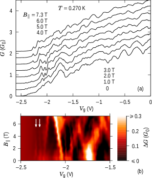
If weakly bound states are formed, calculations show that the exchange interaction creates a spin-imbalance below the first conductance plateau Rejec and Meir (2006). This prediction is supported by a large number of experiments carried out for GaAs QPCs *[See; e.g.; thereview][; andreferencestherein.]Micolich2011. Figure 3 shows the effect of an in-plane magnetic field on our device. The spin-splitting of conductance resonances becomes clearly visible. It is evident from Fig. 3(b), that already at T the energy of spin-up level of the lowest mode crosses the energy of spin-down level of the higher channel. However, a magnetic field that is sufficient to separate the spins, does not change the shape and location of weaker conductance resonances which are observed near pinch-off (marked with arrows). The same key feature was observed also for a quasi-ballistic GaAs quantum wire in the vicinity of a so-called “0.7-anomaly” Czapkiewicz et al. (2008).
We thus find a magnetized regime below the first conduction resonance, in agreement with a picture of spin-polarized charge droplets formed within the QPC Ihnatsenka and Zozoulenko (2007). On the other hand, for (in units) the spin degeneracy of transport channels may be spontaneously lifted without the appearance of localized states Jaksch et al. (2006); Lassl et al. (2007). By combining bias dependence with magnetic field data shown in Fig. 3 we have been able to determine the effective Landé factor at . We have found that in remarkable agreement with bulk value reported for CdTe Oestreich et al. (1996).
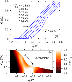
An additional argument for natural formation of an open dot in our device is provided by the conductance data measured for large source-drain voltages (). Calculations suggest Ihnatsenka et al. (2007), that if a weakly bound state is present in the constriction, its local density of states follows Fermi energy when gate voltage is changed. As a result, when electrons travel only in one direction (at finite biases), the pinning of the resonant level leads to the appearance of a plateau-like feature at on curves Ihnatsenka and Zozoulenko (2009). Such “-anomaly” was measured for rather long ( to m) GaAs quantum wires Cronenwett et al. (2002); Sfigakis et al. (2008); Czapkiewicz et al. (2008), where the weakly bound states were present or were probably induced by strong biasSablikov et al. (2000); Ihnatsenka and Zozoulenko (2009). A similar feature is observed also in our shorter device, as it follows from Fig. 4. The formation of a weak shoulder at with increasing source-drain voltage is marked with an arrow. The shift of the conduction onset towards lower values of and the appearance of “-anomaly” is more clearly visible at the transconductance color map, displayed in Fig. 4(b).
In summary, we have presented low-temperature conductance measurements on short point contact made of a CdTe/CdMgTe quantum well. Many of the observed features are shared by longer GaAs wires with centrally embedded open quantum dots. This suggests the spontaneous formation of potential barriers at the entrance and at the exit of our device. Recently, the disappearance of quantized plateaus and evidence for the formation of quasi-bound states in an asymmetrical GaAs QPC have been also reported Wu et al. (2012) and attributed to an abrupt rise of confining potential along the channel. Our sample is symmetric and constriction is defined by an adiabatic variation of width, so a momentum mismatch is less severe, yet stronger e-e interactions in CdTe may induce a natural bound state considerably easier. This makes cadmium telluride a promising host material for studying the interplay between interference and correlation effects in low dimensions.
We acknowledge the support from the Polish Ministry of Science and Higher Education, project number N202/103936 and partial support by the European Union within European Regional Development Fund (grant Innovative Economy POIG.01.01.02-00-008/08).
References
- van Wees et al. (1991) B. J. van Wees, L. P. Kouwenhoven, E. M. M. Willems, C. J. P. M. Harmans, J. E. Mooij, H. van Houten, C. W. J. Beenakker, J. G. Williamson, and C. T. Foxon, Phys. Rev. B 43, 12431 (1991).
- Berggren and Pepper (2010) K.-F. Berggren and M. Pepper, Phil. Trans. R. Soc. A 368, 1141 (2010).
- Sablikov et al. (2000) V. A. Sablikov, S. V. Polyakov, and M. Büttiker, Phys. Rev. B 61, 13763 (2000).
- Piot et al. (2010) B. A. Piot, J. Kunc, M. Potemski, D. K. Maude, C. Betthausen, A. Vogl, D. Weiss, G. Karczewski, and T. Wojtowicz, Phys. Rev. B 82, 081307 (2010).
- Wróbel et al. (1992) J. Wróbel, F. Kuchar, K. Ismail, K. Lee, H. Nickel, and W. Schlapp, Surface Science 263, 261 (1992).
- Liang et al. (1998) C.-T. Liang, M. Y. Simmons, C. G. Smith, G. H. Kim, D. A. Ritchie, and M. Pepper, Phys. Rev. Lett. 81, 3507 (1998).
- Tkachenko et al. (2001) O. A. Tkachenko, V. A. Tkachenko, D. G. Baksheyev, C.-T. Liang, M. Y. Simmons, C. G. Smith, D. A. Ritchie, G.-H. Kim, and M. Pepper, J. Phys.: Condens. Matter 13, 9515 (2001).
- Amasha et al. (2011) S. Amasha, I. G. Rau, M. Grobis, R. M. Potok, H. Shtrikman, and D. Goldhaber-Gordon, Phys. Rev. Lett. 107, 216804 (2011).
- Hirose et al. (2003) K. Hirose, Y. Meir, and N. S. Wingreen, Phys. Rev. Lett. 90, 026804 (2003).
- Rejec and Meir (2006) T. Rejec and Y. Meir, Nature 442, (2006).
- Ihnatsenka and Zozoulenko (2007) S. Ihnatsenka and I. V. Zozoulenko, Phys. Rev. B 76, 045338 (2007).
- Song and Ahn (2011) T. Song and K.-H. Ahn, Phys. Rev. Lett. 106, 057203 (2011).
- Shchamkhalova and Sablikov (2007) B. S. Shchamkhalova and V. A. Sablikov, J. of Phys.: Condens. Matter 19, 156221 (2007).
- Renard et al. (2008) V. T. Renard, O. A. Tkachenko, V. A. Tkachenko, T. Ota, N. Kumada, J.-C. Portal, and Y. Hirayama, Phys. Rev. Lett. 100, 186801 (2008).
- Micolich (2011) A. P. Micolich, J. Phys.: Condens. Matter 23, 443201 (2011).
- Czapkiewicz et al. (2008) M. Czapkiewicz, P. Zagrajek, J. Wróbel, G. Grabecki, K. Fronc, T. Dietl, Y. Ohno, S. Matsuzaka, and H. Ohno, Europhys. Lett. 82, 27003 (2008).
- Jaksch et al. (2006) P. Jaksch, I. Yakimenko, and K.-F. Berggren, Phys. Rev. B 74, 235320 (2006).
- Lassl et al. (2007) A. Lassl, P. Schlagheck, and K. Richter, Phys. Rev. B 75, 045346 (2007).
- Oestreich et al. (1996) M. Oestreich, S. Hallstein, A. P. Heberle, K. Eberl, E. Bauser, and W. W. Rühle, Phys. Rev. B 53, 7911 (1996).
- Ihnatsenka et al. (2007) S. Ihnatsenka, I. V. Zozoulenko, and M. Willander, Phys. Rev. B 75, 235307 (2007).
- Ihnatsenka and Zozoulenko (2009) S. Ihnatsenka and I. V. Zozoulenko, Phys. Rev. B 79, 235313 (2009).
- Cronenwett et al. (2002) S. M. Cronenwett, H. J. Lynch, D. Goldhaber-Gordon, L. P. Kouwenhoven, C. M. Marcus, K. Hirose, N. S. Wingreen, and V. Umansky, Phys. Rev. Lett. 88, 226805 (2002).
- Sfigakis et al. (2008) F. Sfigakis, C. J. B. Ford, M. Pepper, M. Kataoka, D. A. Ritchie, and M. Y. Simmons, Phys. Rev. Lett. 100, 026807 (2008).
- Wu et al. (2012) P. M. Wu, P. Li, H. Zhang, and A. M. Chang, Phys. Rev. B 85, 085305 (2012).