Pure spin current in a two-dimensional topological insulator
Abstract
We predict a mechanism to generate a pure spin current in a two-dimensional topological insulator. As the magnetic impurities exist on one of edges of the two-dimensional topological insulator, a gap is opened in the corresponding gapless edge states but another pair of gapless edge states with opposite spin are still protected by the time-reversal symmetry. So the conductance plateaus with the half-integer values can be obtained in the gap induced by magnetic impurities, which means that the pure spin current can be induced in the sample. We also find that the pure spin current is insensitive to weak disorder. The mechanism to generate pure spin currents is generalized for two-dimensional topological insulators.
pacs:
75.76.+j; 72.80.Vp; 03.65.VfSince graphene, a single-layer honeycomb lattice of carbon atoms, has been prepared laboratorially by Novoselov et al.,Novoselov et al. (2004) it has attracted considerable attentions due to its novel properties in condensed matter physics and potential applications in devices. Geim and Novoselov (2007); Geim (2009); Neto et al. (2009); Beenakker (2008); Abergel et al. (2010); Sarma et al. (2011); Sun and Xie (2010); Zhang et al. (2005); Williams et al. (2007) Graphene is the first independent two-dimensional (2D) crystal that has been experimentally achieved, which leads to new interests in 2D systems. For example, the Kane-Mele model, a quantum spin Hall effect (QSHE) was first proposed in graphene with spin-orbital coupling, which is the first example of topological insulator.Kane and Mele (2005a, b) Topological insulators are time-reversal symmetric systems whose intrinsic spin-orbit coupling (SOC) opens a bulk gap while generating the Kramers doublet of edge states owing to the nontrivial invariants of the occupied bands. The edge states force electrons with opposite spin to flow in opposite directions along the edges of the sample, which lead to quantized spin Hall conductance. However, the intrinsic SOC in realistic graphene is quite weak and the gap opening was small, so the QSHE in graphene is difficult to be observed.Yao et al. (2007) Nevertheless, recently a monolayer honeycomb lattice of silicon called silicene has been synthesized and attracts much attention.Lalmi et al. (2010); Feng et al. (2012); Liu et al. (2011); Ezawa (2012) Silicene has a relatively large intrinsic spin-orbit gap of , as makes experimentally accessible the Kane-Mele type QSHE.Liu et al. (2011)
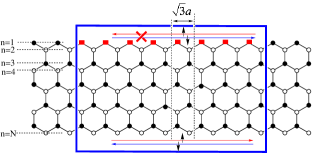
The development of the topological insulator opens a new and powerful way for the spintronic applications due to its spin-dependent edge states. How to generate pure spin currents in low-dimensional systems is the main challenge in the field of spintronics. The aim of this work is to propose a method for generating a pure spin current in a 2DTI. In this Letter, as a concrete example, we theoretically study the electron transport in Kane-Mele model with magnetic doping at one edge, as shown in Fig. 1. Most of the results are also applicable to general 2DTIs. Before presenting our detailed calculations, we first analyze why pure spin current can be generated in the present device. The intrinsic SOC which originates from intra-atomic SOC, converts the sample into a topological insulator with a QSHE.Kane and Mele (2005a) The gapless edge states are protected by time-reversal symmetry and is thus robust to non-magnetic impurities that do not break this symmetry. But a pair of edge states are destroyed when magnetic impurities exist on this corresponding edge (see Fig. 1). Because another pair of edge states, with opposite spins containing opposite propagation directions, are still protected by time-reversal symmetry, we can observe a pure spin current in the sample, which is confirmed by our following calculations.
In the tight-binding representation, we consider the Kane-Mele Hamiltonian defined on a honeycomb lattice:Kane and Mele (2005a, b)
| (1) | |||||
The symbols and denote the nearest and the next-nearest neighbors, respectively, and (or ) denotes spin index. The first term is the nearest-neighbor hopping. The second term describes the intrinsic SOC. Here the site-dependent Haldane phase factorKane and Mele (2005a) is defined as , where denotes the vector from one atom to one of its nearest neighbors. is a Pauli matrix describing the electron’s spin. The third term is a nearest neighbor Rashba SOC term, which can be produced by applying an electric field perpendicular to the sheet. The fourth term is a staggered sublattice potential . It is interesting to notice that, Eq. (1) is almost applicable to silicene except for the Rashba SOC term, which is present between the next-nearest neighbors in silicene but between the nearest neighbors in our model. The focus of this work is the introduction of magnetic impurities (red square dots in Fig. 1) on the uppermost zigzag chain of the sample ,
| (2) |
where is the strength of exchange interaction induced by the magnetic impurities. This term breaks the local time reversal symmetry on the upper edge.
In the following numerical calculations, we use the hopping energy as the energy unit. The width is chosen as in all calculations and the nearest neighbor atom-atom distance is . The strengths of the intrinsic SOC, the Rashba SOC and the staggered sublattice potential are , , and , respectively. These parameters define the system as a two-dimensional topological insulator.Kane and Mele (2005a)
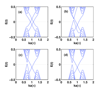
First, we investigate the energy subbands obtained by solving the lattice model in strip geometry, as shown in Fig. 2. In the pure case (, Fig. 2(a)), the edge states traverse the energy gap in pairs. The gapless edge states are robust against small non-magnetic perturbations since they are protected by time reversal symmetry.Kane and Mele (2005a) However, in the presence of magnetic impurities (, Fig. 2(b)-(d)) at the upper edge, the corresponding pair of gapless edge states is destroyed and a gap can be opened due to the local time reversal symmetry breaking. Moreover, the magnitude of the gap opened by the magnetic impurities increases with enhanced , and can reach for . Another pair of gapless edge states, still protected by time reversal symmetry, persist on that edge without magnetic impurities. But the electron-hole symmetry is broken in the preserved gapless edge states, which cross at even for a very small value of .
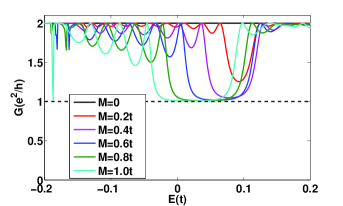
Next, we examine the influence of the magnetic impurities on the conductance of the system, as shown in Fig. 3. The two-terminal conductance of the system can be calculated by the nonequilibrium Green’s function method and the Landauer-Büttiker formula , where is the line-width function and is the retarded Green function with the Hamiltonian in the center region .Ren et al. (2006) The self-energy due to the semi-infinite lead- can be calculated numerically.Sancho et al. (1985) In the case of , the quantized conductance plateau appears, with the plateau value coming from the contributions of two pairs of the gapless edge states. For greater values of , the conductance plateau is suppressed and evolves into a conductance plateau in the energy gap opened by the magnetic impurities. The conductance plateau is only contributed from the gapless edge states at the lower edge without magnetic impurities, which can be seen from Fig. 4. Without magnetic impurities (), there are two pairs of perfect edge states with opposite spins at two edges of the sample, so the currents through the sample is spin unpolarized. However, when the gapless edge states at the upper edge are destroyed by magnetic impurities (), the spin-velocity locked channels persist only at the lower edge of the sample. Therefore, the current in the sample consists of the opposite spins moving in opposite directions that is called pure spin current, which is just the aim of the present work. For a definite arrangement of bias voltage, there remains only, say, right going channels with spin up working. Moreover, the pure spin current in the sample is really invariant under time reversal.
To test the above arguments in a more direct way, we also studied the spin-resolved conductance and spin polarization when the magnetic impurities exist on the upper edge of the sample. For the sake of simplicity, we assume that in the leads, the staggered sublattice potential, the intrinsic and Rashba SOC do not exist, i.e., the Hamiltonian of lead- is simply
| (3) |
The spin-resolved conductance matrix can be written as
| (6) |
which can also be calculated by generalized Landauer formula for spin transport. The conductance and can be obtained when we assume that only spin-up electrons are injected from the left lead into the sample and collected in the right lead. We can also calculate and in the same way by assuming only spin-down electrons are injected from the left lead. The total conductance and the spin polarization in lead- can be respectively defined asBellucci and Onorato (2008); Ming et al. (2011)
| (7) |
and
| (8) |
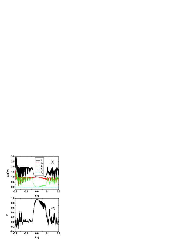
Fig. 5 (a) and (b) show the spin-resolved conductance and spin polarization versus the energy for . In Fig. 5 (a), the total conductance manifests itself with the plateau value due to the presence of the magnetic impurities on the upper edge of the central region. Due to the topological nature of the edge states, this plateau is insensitive to the mismatch between the sample and the leads. We can also find that the spin-up and spin-down electrons are not mixed when they transport through the sample, i.e., . The spin polarization can almost reach in the energy gap opened by the magnetic impurities [see Fig. 5 (b)] because the spin-up electron can fully transport through the sample while the spin-down electron can hardly transport through the sample in the gap [see Fig. 5 (a)]. Beyond the gap, due to the conduction band mismatch between the central region and the leads, there are resonant tunneling peaks in the conductance beyond the gap induced by the magnetic impurities, as shown in Fig. 3 and Fig. 5.
Finally, we examine the non-magnetic disorder effect on this spin-polarized conductance plateau . Due to disorder, random on-site potential is added for each site in the central region, where is uniformly distributed in the range with the disorder strength . Fig. 6 (a) and (b) show the conductance versus the energy at the disorder strength and versus the disorder strength at the energy , respectively. The results show that the quantum plateau of is very robust against non-magnetic disorder because of the topological origin of the edge states. The quantum plateau maintains its quantized value very well even when reaches . The robust and stable plateau of means that the pure spin current of the system is insensitive to weak disorder and protected by time-reversal symmetry. In addition, even for a large disorder strength (e.g., from to ), the conductance is increased rather than decreasing with the increasing disorder strength. This is because although the strong disorder weakens the edge states, it also result in the mobility of the energy band structure,Zhang et al. (2012) so the value of increases in the range of to . With further increasing of the disorder strength, the conductance gradually reduce to zero, the system eventually enters the insulating regime.
In summary, we predict a new mechanism to generate a pure spin current in a two-dimensional topological insulator. As the magnetic impurities exist on one edge of the sample, the corresponding gapless edge states is destroyed but another pair of gapless edge states with opposite spin are protected by time-reversal symmetry. So a pure spin current with the spin-up and spin-down carriers moving in opposite directions can be observed in the system. Moreover, the pure spin current has also been found to be robust against non-magnetic disorder. The mechanism to generate pure spin currents can be generalized for two-dimensional topological insulators, such as HgTe/CdTe quantum well and silicene nanoribbons.
This work was supported by National Natural Science Foundation of China (Grant Nos. 11047184, 11104059, No. 61176089) and Hebei province Natural Science Foundation of China (Grant No. A2011208010).
References
- Novoselov et al. (2004) K. S. Novoselov, A. K. Geim, S. V. Morozov, D. Jiang, Y. Zhang, S. V. Dubonos, I. V. Grigorieva, and A. A. Firsov, Science 306, 666 (2004).
- Geim and Novoselov (2007) A. K. Geim and K. S. Novoselov, Nat. Mater. 6, 183 (2007).
- Geim (2009) A. K. Geim, Science 324, 1530 (2009).
- Neto et al. (2009) A. H. C. Neto, F. Guinea, N. M. R. Peres, K. S. Novoselov, and A. K. Geim, Rev. Mod. Phys. 81, 109 (2009).
- Beenakker (2008) C. W. J. Beenakker, Rev. Mod. Phys. 80, 1337 (2008).
- Abergel et al. (2010) D. S. L. Abergel, V. Apalkov, J. Berashevich, K. Ziegler, and T. Chakraborty, Adv. Phys. 59, 261 (2010).
- Sarma et al. (2011) S. D. Sarma, S. Adam, E. H. Hwang, and E. Rossi, Rev. Mod. Phys. 83, 407 (2011).
- Sun and Xie (2010) Q.-F. Sun and X. C. Xie, Phys. Rev. Lett. 104, 066805 (2010).
- Zhang et al. (2005) Y. Zhang, Y.-W. Tan, H. L. Stormer, and P. Kim, Nature (London) 438, 201 (2005).
- Williams et al. (2007) J. R. Williams, L. Dicarlo, and C. M. Marcus, Science 317, 638 (2007).
- Kane and Mele (2005a) C. L. Kane and E. J. Mele, Phys. Rev. Lett. 95, 146802 (2005a).
- Kane and Mele (2005b) C. L. Kane and E. J. Mele, Phys. Rev. Lett. 95, 226801 (2005b).
- Yao et al. (2007) Y. Yao, F. Ye, X.-L. Qi, S.-C. Zhang, and Z. Fang, Phys. Rev. B 75, 041401(R) (2007).
- Lalmi et al. (2010) B. Lalmi, H. Oughaddou, H. Enriquez, A. Kara, S. Vizzini, B. Ealet, and B. Aufray, Appl. Phys. Lett. 97, 223109 (2010).
- Feng et al. (2012) B. Feng, Z. Ding, S. Meng, Y. Yao, X. He, P. Cheng, L. Chen, and K. Wu, cond-mat/arXiv:1203.2745 (2012).
- Liu et al. (2011) C.-C. Liu, W. Feng, and Y. Yao, Phys. Rev. Lett. 107, 076802 (2011).
- Ezawa (2012) M. Ezawa, cond-mat/arXiv:1203.0705 (2012).
- Ren et al. (2006) W. Ren, Z. Qiao, J. Wang, Q.-F. Sun, and H. Guo, Phys. Rev. Lett. 97, 066603 (2006).
- Sancho et al. (1985) M. P. L. Sancho, J. M. L. Sancho, and J. Rubio, I. Phys. F: Met. Phys. 15, 851 (1985).
- Bellucci and Onorato (2008) S. Bellucci and P. Onorato, Phys. Rev. B 77, 075303 (2008).
- Ming et al. (2011) Y. Ming, J. Gong, and R. Q. Zhang, J. Appl. Phys. 110, 093717 (2011).
- Zhang et al. (2012) Y.-Y. Zhang, R.-L. Chu, F.-C. Zhang, and S.-Q. Shen, Phys. Rev. B 85, 035107 (2012).