White Light Interferometry for Quantitative Surface Characterization in Ion Sputtering Experiments
Abstract
White light interferometry (WLI) can be used to obtain surface morphology information on dimensional scale of millimeters with lateral resolution as good as 1 m and depth resolution down to 1 nm. By performing true three-dimensional imaging of sample surfaces, the WLI technique enables accurate quantitative characterization of the geometry of surface features and compares favorably to scanning electron and atomic force microscopies by avoiding some of their drawbacks.
In this paper, results of using the WLI imaging technique to characterize the products of ion sputtering experiments are reported. With a few figures, several example applications of the WLI method are illustrated when used for (i) sputtering yield measurements and time-to-depth conversion, (ii) optimizing ion beam current density profiles, the shapes of sputtered craters, and multiple ion beam superposition and (iii) quantitative characterization of surfaces processed with ions.
In particular, for sputter depth profiling experiments of 25Mg, 44Ca and 53Cr ion implants in Si (implantation energy of 1 keV per nucleon), the depth calibration of the measured depth profile curves determined by the WLI method appeared to be self-consistent with TRIM simulations for such projectile-matrix systems. In addition, high depth resolution of the WLI method is demonstrated for a case of a Genesis solar wind Si collector surface processed by gas cluster ion beam: a 12.5 nm layer was removed from the processed surface, while the transition length between the processed and untreated areas was 150 m.
pacs:
06.30.Bp, 07.60.Ly, 61.80.Jh, 79.20.RfI Introduction
In many experiments designed to determine sputtering yields (SY) of various materials under specific ion bombardment conditions, uncertainties in ion beam parameters can propagate and result in uncertain sputtering yield values 1 . For example, it can be challenging to determine shapes of ion beam profiles and the corresponding operational current densities, especially when the projectile energy goes below 1 keV and then further approaches the sputtering threshold. Moreover, under such conditions, the focusing of the ion beam is in question, and the relative spread in the initial kinetic energy distribution of ions 2 can have strong influence on experimental results 3 ; 4 .
The other aspect that has a great impact on the final results is the method used for quantitative analysis of the surface, being commonly scanning electron and atomic force microscopy (SEM and AFM, respectively). Both techniques are valuable, but each has its own limitations, when used for surface morphology characterization. The AFM can obtain three-dimensional (3D) imaging and thus the cross section profiles for sputtering craters, but AFM has rather narrow ranges in the maximum lateral and especially depth scanning. The SEM has much greater flexibility in the size of field-of-view with large depth of focus, but obtaining 3D imaging is cumbersome 5 . Another technique widely used in secondary ion mass spectrometry is the Stylus Profilometry. This technique is popular because of its simplicity, but it is a coarser contact tool able to scan along a single line at a time, which would make 3D surface imaging extremely time consuming. The qualifier ”coarser” means the Stylus has difficulty measuring surface features of high aspect ratio or of size comparable with its characteristic tip size that implies a tip radius along with a tip angle 6 . It should be mentioned that in the case of the trace analysis mass spectrometry (our case), it is undesirable to have a sample to be analyzed in physical contact with a Stylus tip, which may contaminate or even scratch the surface. All these facts make researchers to look for alternative methods for surface topography measurements. In this regard, the optical interference methods seem to be natural. It is known that the main drawback of an optical technique (utilizing geometrical optics) is the limited lateral resolution against SEM and AFM. This limitation is of fundamental nature in that a surface feature of characteristic size less than (where is a light wavelength) cannot be resolved correctly. On the other hand, the interference approach gives a fascinating depth resolution of less than 1 nm.
This work reports on application of the white light profilometry based on a Mirau interferometer (which is common for most of the commercial instruments) to characterize solid surfaces eroded in ion sputtering experiments. A few examples of applying this method are provided when used for (i) characterization of ion beam profiles and crater shapes yielding accurate SY estimates, (ii) overlap alignment of a multiple ion beams system, (iii) time-to-depth calibration in sputter depth profiling, and (iv) characterization of surface processing of materials by ion beams. For sputtering yield and rate estimates, the presented results demonstrate an alternative experimental approach to generate reference data for many materials and technological applications 4 ; 7 ; 8 ; 9 ; 10 ; 11 ; 12 ; 13 under bombardment with both commonly used atomic ions and relatively new molecular and cluster ions and help to resolve the problem of time or primary ion fluence to depth conversion.
In regard to mass spectrometry experiments, investigation of WLI benefits is practically important for us, since WLI as non-contact optical technique is attractive for implementing as an in-situ characterization tool.
II Material and methods
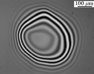
Mirau interferometry is an optical technique that measures the phase shift between the reference light signal and the light reflected from the sample surface. It provides an optical micrograph onto which constructive and destructive interference fringes (light/dark) are superimposed. The fringes are used to reconstruct the three-dimensional surface profile. A white light source supplies a broad spectrum light. This eliminates the problem associated with certain specimen features where the correct interference order cannot be determined. The lateral resolution of the WLI probe is determined mostly by the chosen numerical aperture of the objective (limited to at numerical aperture 1). Once the best focus is found by mechanical positioning of the sample stage and the objective (corresponding to the brightest and strongest interference fringes, see Fig.1), a piezo transducer inside the objective performs vertical scanning of heights over a specified range. Then an array of phase shifts between the reference signal, with constant optical path, and the signal, with an optical path which depends on the depth, is used to reconstruct true 3D surface topography and morphology. At first glance, it seems that optically transparent films on a reflective substrate pose a serious problem for WLI. If a material is transparent for given wavelength , there is always a phase shift (optical path length change) due to multiple passes of the light inside a film of refractive index , which may yield artifacts in a 3D topographic image. At the same time, the phase shift allows one to distinguish between the transparent film response and the signal originated from the reflective base. By separating these two responses (either directly 14 or by a special post-processing algorithm 15 ) and paying attention to an absorption characteristic (which can be obtained independently) 16 , one can measure a transparent/semitransparent film thickness starting at an order of 10 nm or higher (up to several m), so that the drawback may turn out to be an additional advantage. Information on Mirau WLI can be found in Refs.17 ; 18 in great details.
In the experiments presented here a MicroXAM-1200 profilometer controlled via MapVue AE software was employed. The images were visualized using the SPIP software. Before every measurement, the profilometer was calibrated laterally by a precise sub-mm ruler and vertically by 500 nm step AFM standard from Ted Pella, Inc.
In the examples of application of the WLI to ion sputtering experiments that follow, small (1010 mm2) pieces of Si(001) (MEMC Electronics and Unisil), and Cu(110) and Cu(111) (MTI Corporation) monocrystals were utilized. In this context, these Si and Cu samples (which are uniform and nontransparent materials) do not have the ”transparent sample” problem described above. In addition, it seems that in many sputtering experiments, including the present study, shapes of removed craters, spots, etc. can be classified as low gradient or step-like, which favors WLI applicability 19 .
III Results and discussion
1. Craters and ion beam profiles measurements to estimate Sputtering Yield
As an alternative to the known and widely employed method for estimating sputtering yields using mass-loss method, based on direct weighing or quartz microcrystal balance 20 , we propose to use the WLI method for direct visualization of the sputtered ion beam spots or craters obtained by static sputtering or by raster scanning of an ion beam, respectively. For low energy ion beam irradiation, WLI can verify whether or not the entire beam was confined to the sample of interest. By combining the WLI visualization with precise measurements of the total ion current by a Faraday cup, the SY and the operating current density can be obtained simultaneously. Besides, this approach appears to be very helpful in estimating the extent of undesirable ”wings” of the ion beam profile so that, as a feedback, it guides the alignment of an ion beam source. The sputtering yield is then estimated using the following expression
| (1) |
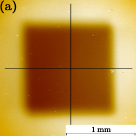
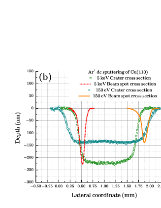
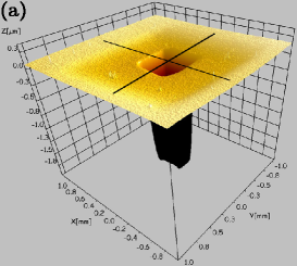
where , direct current (dc) current of an ion beam; , time of sputtering; , mass of a matrix atom in grams; , density; , the elementary charge. is the volume of the removed sample material obtained by means of the WLI measurement. Volume calculations can be performed either by using a histogram of heights typically available through an interferometer post-processing software called SPIP by Image Metrology that works with files type generated by MapVue AE or by three dimensional integration based on cross sections in two orthogonal directions centered on the eroded surface area (black lines in Fig.2a).
Figure 2 compares longitudinal cross sections of a spot (red dotted line) of a normally incident static 5 keV Ar+ ion beam against a crater (green open squares) obtained by 100100 pixels digital raster scanning of the same ion beam over the surface of a Cu(110) monocrystal. The curve corresponding to the static beam overlaps one edge of the crater to demonstrate how raster scan of the ion beam generates the crater during sputter depth profiling. Good alignment of the ion beam column manifests itself in a symmetric beam profile and FWHM of 120 m at a total current of 2 A. The WLI approach allows one to characterize the ion sputtering with the same normally incident ion beam decelerated to 150 eV by the target potential. In this case, the cross section of the static beam spot is shown by an orange solid line, and the crater cross section is shown by cyan open circles. The ion column allowed delivery of the same 2 A of Ar+ current on the target because the deceleration of the beam from the nominal 5 keV energy to 150 eV occurred in the immediate vicinity of the target, and in such a way that its optimal focusing was maintained by an electrostatic lens (FWHM of 150 m in Fig.2b proves that) 21 . The sputtered crater has in this case a larger lateral size because the deflection voltages of the raster-generating octupole were kept unchanged for the two primary ion impact energies, resulting in additional beam swinging due to the target potential.
Based on the WLI data, sputtering yields of Cu(110) at 5 keV and 150 eV ion impact energies were determined. An obtained SY value of 1.8 at/ion for the former case was in good agreement with literature data 22 . For the latter one, the sputtering yield was 0.2 at/ion. The SY values for Cu(111) at 50, 100, and 150 eV were also determined as 0.13, 0.27, and 0.42 at/ion, respectively. The measured energy spread of the low energy system 21 is 23 eV.
2. Multiple beam system alignment and time-to-depth conversion
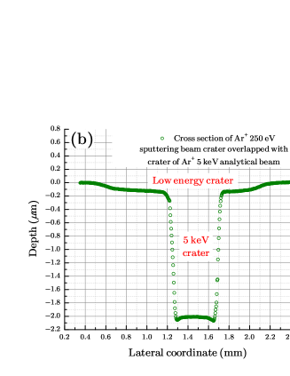
In our previous work, we have introduced and demonstrated a new variant of dual-beam (DB) sputter depth profiling for time-of-flight secondary ion mass spectrometry (TOF SIMS), where we aimed at improving the depth resolution by using a normally incident low-energy direct current ion beam for sputtering, in combination with obliquely incident fine focused pulsed ion beam for TOF SIMS analysis. The benefit of such an arrangement of the sputtering ion beam is two-fold: its low (a few hundred eV) energy reduces ion beam mixing, and its normal impact angle reduces surface roughening. To make this concept work, it is needed to precisely overlap the crater created by raster scanning the low energy dc ion beam with the area probed by the pulsed analysis ion beam. Moreover, (i) most of the bottom of the low energy crater must be flat (Fig.2b), and (ii) the analysis area must be confined within that flat part, in order to avoid distortions in the depth profile due to probing sloped areas or crater walls. This can only be achieved by thorough optimization of both ion beams (current density profiles and focusing) as well as precise control of their steering. The WLI technique helps to make this multi-step alignment much easier.
Results of the WLI characterization presented in Fig.3 give straightforward answers regarding mutual positioning of sputtering and analysis ion beams by showing two craters produced by raster scanning of these beams in dc mode. The deep and narrow crater seen in Fig.3 was made by the analysis beam (5 keV Ar+ ions with 60∘ incident angle). The wide and shallow crater was made by a normally incident 500 eV Ar+ ion beam. Fig.3 demonstrates that the 5 keV Ar+ probing in the DB mode was conducted on the flat bottom part of the crater created by the low energy sputtering ion beam.
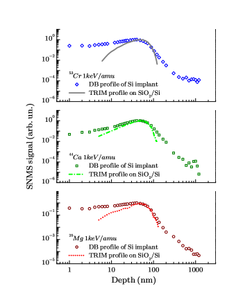
Another important application of the WLI method to sputter depth profiling is exemplified by the sputtering time to sputtered depth calibration procedure applied to this particular experiment. The samples analyzed here were pieces of Si(001) wafer implanted with 25Mg+, 44Ca+ and 53Cr+ ions at energy of 1 keV per atomic mass unit (25 keV for 25Mg, 44 keV for 44Ca and 53 keV for 53Cr, all at 31013 ions/cm2 fluence) fabricated by Leonard Kroko Inc. A TOF MS analysis of these samples was performed by laser post-ionization of sputtered neutrals (secondary neutral mass spectrometry, SNMS) using resonantly enhanced multi-photon ionization to simultaneously detect all isotopes of Mg, Ca and Cr 23 . This was an experiment on sputter depth profiling which started in the DB mode as described above but, after the concentration peaks of the implants were passed (that is, after 170 nm on the depth scale in Fig.3, see also Fig.4), the experiment continued in the single beam (SB) mode by switching off the low energy sputtering beam, while the analysis beam performed both the ion milling (in dc mode) and the analysis (in pulsed mode). The higher energy (5 keV) and 60∘ incidence of the analysis beam allowed us to reduce the time needed for measuring the trailing edge of the implant depth profiles where high depth resolution was not needed. The calibration procedure involved: (i) the WLI measurements of the depths of craters created by both ion beams, as shown in Fig.3, (ii) ion current measurements of both these beams with the Faraday cup, and (iii) calculating depth scale based on the total sputtering time with either of the two beams and the corresponding WLI measurements of crater depths. To compare this depth calibration with a model estimate, TRIM simulations for 1 keV/amu ions of the same Mg, Ca and Cr isotopes implanted in a Si matrix with SiO2 of 2 nm on top were performed. After that, the experimental and simulated data were compared on the same plot, as shown in Fig.4. This comparison revealed very good agreement between the depths of Ca and Mg implant peak concentrations determined by the WLI-based depth calibration and simulated by TRIM. In the case of Cr, the shift between simulated and experimentally measured peak was 5 nm. Thus, the sputtering time to depth calibration using the WLI measurements proved to be satisfactorily accurate. It proved also that, if a depth profile is made purely in SB manner, an elemental peak distribution appears to lie deeper (under the same time-to-depth conversion procedure by WLI) as compared to DB results shown in Fig.4. This peak depth overestimation leads to an error in the fluence value obtained by integration of the depth profile curve. This issue is not discussed here, since this fact is obvious and lies beyond the scope of this paper.
3. Quantitative characterization of ultra-shallow surface processing with cluster ion beam
In this example, the depth resolution of the WLI technique applied to characterization of Si surfaces irradiated with gas cluster ion beams (GCIB) is demonstrated. The GCIB in these sputtering experiments was an argon cluster beam Ar with =2000, where corresponds to the number of atoms in the peak distribution and, in general, can lie between 200 and 10000 24 ; 25 . Irradiating materials surfaces with such cluster ions causes two unique effects. First, because the impact energy of such projectiles equals to their kinetic energy divided by the number of constituent atoms, for a 20 keV Ar, for example, it will be only 10 eV/Ar, which significantly reduces the penetration of individual Ar atoms into the target and the sputtering process starts to strongly depend on the collective effects of many such impacts. In essence, for GCIB irradiation, the sample damage is confined to a narrow near-surface layer. Another effect is the surface ”polishing” (or planarization), which manifests itself in a reduced roughness of the irradiated surfaces. To summarize, at normal incidence the GCIB irradiation can literally ”shave off” topmost layers from a target with minimal alteration of underlying regions.
These two effects are very beneficial for our efforts on quantitative analyses of the Genesis mission 26 solar wind (SW) collectors by resonance ionization mass spectrometry 23 . The Genesis mission samples present a serious analytical challenge because of abundant contamination which blanketed the collectors surface after the crash landing of the Genesis sample return capsule. In addition to the crash-derived contamination, such as terrestrial dust particles, a highly refractory organic/silicon film, known as the ”brown stain” 27 , covers the top of Genesis samples. While conventional methods such as megasonic cleaning with ultrapure water removes particulates 1 m loosely connected to surface 28 , the remaining contamination must be dealt with differently. The GCIB processing of surfaces of Genesis collectors has the potential to ”shave off” this contamination blanket with minimal losses of the implanted SW species 29 . To our knowledge, this is possibly the most advanced cleaning method proposed so far for uniform removal of surface contamination.
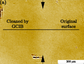
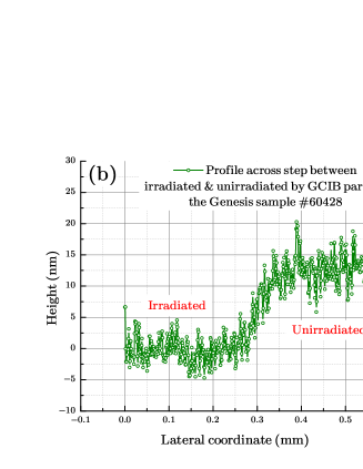
In this WLI example the GCIB processed surface of the Genesis 60428 Si coupon is characterized in order to measure the exact depth removed. Currently, by measuring 24Mg, 40Ca and 52Cr solar wind distributions by DB SNMS, we know that the surface contamination covers the first 10 nm of the depth profile 30 . By using the GCIB process to reduce the surface contamination, the contribution of contamination to the depth profile is significantly decreased, resolving the SW profile from it and permitting a more accurate integration of the SW depth profile curve to obtain elemental abundance fluences. Thus, the precise thickness of the layer removed by GCIB is critical.
GCIB processing conditions on the Genesis 60428 Si coupon were as follows: operating current of 68 A, GCIB raster area of 6.410-3 m2, GCIB exposed Si surface area of 2.910-5 m2, and the sample processing time under GCIB s (where 153 s is the total time during which GCIB source was switched on and raster scanned).
The measurement depicted in Fig.5 shows that the surface layer removed by GCIB irradiation was as low as 12.5 nm. At the same time, the length of the transition region between irradiated and non-irradiated areas of the sample is as long as 150 m. This length is on the order of the full lateral scan of an AFM, and makes it essentially impossible to find such a step by means of AFM, while the depth is at the resolution limit of the best Stylus Profilometer, emphasizing the high value of the WLI method. If we assume that, originally, the sample consists of only Si and use the literature data for sputtering yield of Si under a 20 keV Ar cluster ion beam (=41.5 atoms per cluster ion 31 ), the thickness that should have been removed would be 8.5 nm. This estimate proves indirectly the presence of an extra layer that may contain submicron particulates, the ”brown stain”, and the native silicon oxide layer before the GCIB processing.
IV Conclusions
The benefits of the white light optical profilometry based on a Mirau interferometer were demonstrated when it is applied to problems of quantitative characterization of ion sputtered surfaces. The key advantages of this technique are high depth resolution in combination with flexible lateral field-of-view and the capability of true three-dimensional surface topography reconstruction.
Examples to prove the power of this method were provided here. In particular, it was demonstrated how to use the WLI approach to determine sputtering yields of copper and silicon irradiated by ultralow energy argon ions over confined eroded area of controlled geometry. Such measurements can be done both on focused static beam spots (10 m dia.) and on mm-scale raster scan craters with high extent of averaging the sputtering characteristic. In addition, the WLI technique can significantly help with alignment of ion columns with multiple overlapping or superimposed ion (or ion and laser) beams, as demonstrated in presented example with the dual-beam sputter depth profiling.
Thus, the WLI technique facilitates better fundamental understanding of sputtering processes at ultra-low energies by helping to accurately determine sputtering yields (and by addressing problems of preferential sputtering), and by helping with precise conversion of ion fluence or sputtering time into depth. Moreover, it lends scientists an ability to precisely characterize and, ultimately, to control materials’ surface topography formed by ion sputtering under a wide variation of conditions (eV to tens of keV impact energy or atomic/cluster/molecular projectile species), which is a great benefit for ion sputtering based materials synthesis or characterization.
V Acknowledgments
The authors would like to thank Dr. James Norem (Argonne National Laboratory, USA) for providing the Cu monocrystals, and Profs. Isao Yamada and Noriaki Toyoda (University of Hyogo, Japan) for GCIB processing of the Genesis sample surface. This work was supported under Contract No. DE-AC02-06CH11357 between UChicago Argonne, LLC and the U.S. Department of Energy and by NASA through grants NNH08AH761 and NNH08ZDA001N.
References
- (1) K. Wittmaack, Phys. Rev. B 68, 235211 (2003).
- (2) M. Zeuner, H. Neumann, F. Scholze, D. Flamm, M. Tartz, F. Bigl, Plasma Sources Sci. Technol. 7, 252 (1998).
- (3) A. Barna, M. Menyhard, L. Kotis, G.J. Kovacs, G. Radnoczi, A. Zalar, P. Panjan, J. Appl. Phys. 98, 024901 (2005).
- (4) S.-M. Wu, R. van de Kruijs, E. Zoethout, F. Bijkerk, J. Appl. Phys. 106, 054902 (2009).
- (5) D.A. Sakseev, E.M. Ershenko, S.V. Baryshev, A.V. Bobyl, D.V. Agafonov, Technical Physics 56, 127 (2011).
- (6) C. O Mahony, M. Hill, M. Brunet, R. Duane, A. Mathewson, Meas. Sci. Technol. 14, 1807 (2003).
- (7) K. Wittmaack, Appl. Surf. Sci. 252, 6413 (2006).
- (8) R. Kolasinski, J. Polk, D. Goebel, L. Johnson, Appl. Surf. Sci. 254, 2506 (2008).
- (9) A. Zalar, J. Kovac, B. Pracek, P. Panjan, M. Ceh, Appl. Surf. Sci. 254, 6611 (2008).
- (10) Z. Insepov, J. Norem, S. Veitzer, Nucl. Instr. Methods Phys. Res. B 268, 642 (2010).
- (11) L. Puech, C. Dubarry, G. Ravel, E. de Vito, J. Appl. Phys. 107, 054908 (2010).
- (12) S. Ho, T. Tamakoshi, M. Ikeda, Y. Mikami, K. Suzuki, J. Appl. Phys. 109, 084908 (2011).
- (13) M. Hada, S. Ninomiya, T. Seki, T. Aoki, J. Matsuo, Surf. Interface Anal. 43, 84 (2011).
- (14) A. Luttge, R.S. Arvidson, J. Am. Ceram. Soc. 93, 3519 (2010).
- (15) M. Conroy, D. Mansfield, Nature Photonics 2, 661 (2008).
- (16) A. Harasaki, J. Schmit, J.C. Wyant, Applied Optics 40, 2102 (2001).
- (17) Y.-Y. Cheng, J.C. Wyant, Applied Optics 24, 804 (1985).
- (18) G.S. Kino, S.S.C. Chim, Applied Optics 29, 3775 (1990).
- (19) F. Gao, R.K. Leach, J. Petzing, J.M. Coupland, Meas. Sci. Technol. 19, 015303 (2008).
- (20) H.H. Andersen, H.L. Bay, Topics in Applied Physics 47, 145 (1981).
- (21) Main techical details on governing the multiple beams system are in I. V. Veryovkin, C. E. Tripa, M. Pellin, Physics Procedia 1, 379 (2008).
- (22) H.E. Roosendaal, Topics in Applied Physics 47, 219 (1981).
- (23) I.V. Veryovkin, C.E. Tripa, A.V. Zinovev, B.V. King, M.J. Pellin, D.S. Burnett, Surf. Interface Anal. 43, 467 (2011).
- (24) I. Yamada, J. Matsuo, N. Toyoda, A. Kirkpatrick, Materials Science and Engineering: R 34, 231 (2001).
- (25) K. Nagato, N. Toyoda, H. Naito, H. Tani, Y. Sakane, I. Yamada, M. Nakao, T. Hamaguchi, J. Appl. Phys. 109, 07B733 (2011).
- (26) D.S. Burnett, B.L. Barraclough, R. Bennett, M. Neugebauer, L.P. Oldham, C.N. Sasaki, D. Sevilla, N. Smith, E. Stansbery, D. Sweetnam, R.C. Wiens, Space Sci. Rev. 105, 509 (2003).
- (27) M.J. Calaway, E.K. Stansbery, K.M. McNamara, 37th Lunar and Planetary Science Conference, Abstract 1420 (2006).
- (28) J.H. Allton, S.J. Wentworth, M.C. Rodriguez, M.J. Calaway, 38th Lunar and Planetary Science Conference, Abstract 2138 (2007).
- (29) B.V. King, I.V. Veryovkin, A.V. Zinovev, C.E. Tripa, M.J. Pellin, N. Toyoda, I. Yamada, M. Schmeling, 41st Lunar and Planetary Science Conference, Abstract 1975 (2010).
- (30) I.V. Veryovkin, C.E. Tripa, A.V. Zinovev, S.V. Baryshev, M.J. Pellin, D.S. Burnett, 42nd Lunar and Planetary Science Conference, Abstract 2308 (2011).
- (31) K. Ichiki, S. Ninomiya, T. Seki, T. Aoki, J. Matsuo, AIP Conf. Proc. 1321, 294 (2011).