Ulta-slow relaxation in discontinuous-film based electron glasses
Abstract
We present field effect measurements on discontinuous 2D thin films which are composed of a sub monolayer of nano-grains of Au, Ni, Ag or Al. Like other electron glasses these systems exhibit slow conductance relaxation and memory effects. However, unlike other systems, the discontinuous films exhibit a dramatic slowing down of the dynamics below a characteristic temperature . is typically between 10-50K and is sample dependent. For the sample exhibits a few other peculiar features such as repeatable conductance fluctuations in millimeter size samples. We suggest that the enhanced system sluggishness is related to the current carrying network becoming very dilute in discontinuous films so that the system contains many parts which are electrically very weakly connected and the transport is dominated by very few weak links. This enables studying the glassy properties of the sample as it transitions from a macroscopic sample to a mesocopic sample, hence, the results provide new insight on the underlying physics of electron glasses.
pacs:
75.75.Lf; 72.80.Ng; 72.20.Ee; 73.40.RwGlassy behavior of the conductivity, , in strongly disordered systems that are characterized by strong electronic interactions were predicted by several groups Grunewald ; pollak1 ; pollak2 ; davies ; vignale . Exciting such a system out of equilibrium leads to an increase in conductivity, , after which the relaxation towards equilibrium is characterized by extremely long times, memory phenomena and aging. Since the slow dynamics are related to their electronic properties these systems were termed electron glasses davies . Experimentally, glassy features were observed in a verity of systems including granular Au adkins , amorphous and poly-crystalline indium oxide films moshe ; ady0 ; ady1 ; ady1_5 ; ady2 , ultrathin Pb films goldman , granular aluminum grenet1 ; grenet2 and thin beryllium films be . A standard way of excitation in these experiments is by applying a gate voltage, , in a MOSFET setup. Conductivity increases for both orientations of followed by very slow relaxation of which is found to follow an approximate logarithmic dependence on time and may be measured over time-scales of days. A typical feature which has been suggested as the hallmark of intrinsic electron glasses zvi_dip is a ”memory dip” (MD) which shows up as a minimum in the curve when is scanned fast compared to the characteristic relaxation time. The dip is centered around the gate voltage at which the sample was allowed to equilibrate.
The origin of the extremely slow relaxation and the memory dip as well as their dependence on parameters such as temperature, bias voltage, carrier concentration etc. are still under debate and more experimental information may help shedding light on the physics of electron glasses. In this letter we present results on the glassy properties of two dimensional discontinuous films. We find that these systems exhibit a dramatic slowing down of the dynamics below a characteristic temperature . For the conductance of the sample exhibits reproducible fluctuations with exponentially growing amplitude as the temperature is lowered indicating that the effective electronic size of the sample has become very small. We discuss the influence of the sample geometry and its effective size on the conductance relaxation properties.
All conductance results presented in this work were obtained by standard 2-wire lock-in techniques performed on thin discontinuous Au, Al, Ag or Ni films prepared by the quench condensation technique, i.e. thermal evaporation on a cryocooled substrate strongin ; aviad1 ; aviad2 . dc techniques were used for comparison in a few cases yielding similar results. For achieving field effect geometry we used a doped Si substrate (that was utilized as a gate electrode) coated by a 0.5 insulating SiO layer. Gold pads were pre-prepared on the substrate so that, together with a shadow mask, they defined a sample area of 0.6mm by 0.6mm. The substrate was then placed on a sample holder within a vacuum chamber. After the chamber was pumped out, the substrate was cooled to cryogenic temperatures and thin layers of Au, Ni, Al or Ag were deposited while monitoring the film thickness and resistance. For thin enough layers this technique yields a film that is discontinuous, consisting of a sub monolayer of metallic grains, 10-20nm in diameter, separated by vacuum as seen in fig. 1. A major advantage of this method is that throughout the entire process of sample growth and measurement the samples are kept in ultra-high vacuum and not exposed to air, thus protecting the grains from oxidation or contamination. This is especially important for nano-grains in which the surface area to volume ratio is very high.
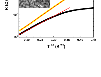
Granular metals which are on the insulating side of the metal-insulator-transition are known to be hopping systems that exhibit resistance versus temperature (R(T)) curves that follow:
| (1) |
Experimentally, between 0.5 and 1 have been reported. In our films eq. 1 is fulfilled only for relatively high T. Fig. 1. depicts the R(T) curves of a gold film and a nickel film. It is seen that for temperatures higher than a characteristic temperature, (in fig 1 for the gold sample and for the Ni sample), we observe a usual Efros Shklovskii ES like dependence (). However, for the conductance depends much weaker on temperature and seems to be approaching saturation at low temperatures.
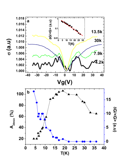
It turns out that T* manifests itself in other transport properties of the sample. As in other electron glasses, after the sample is allowed to equilibrate at a certain gate voltage, for a long time, a MD is observed in conductance versus gate voltage curve. In all our films the MD is accompanied by reproducible conductance fluctuations (see fig. 2). These fluctuations are random, however they are reproducible for sequential experiments performed under similar conditions. Such fluctuations have been observed in the past in indium oxide vladimeso and granular Al grenetmeso electron glasses with dimensions smaller than . We observe these fluctuations for much larger samples. Fig. 2 shows that the rms amplitude of the fluctuations, , of a 0.6*0.6 mm film becomes measurable for and grows exponentially with decreasing temperature. The increase of with lowering T was observed in other systems grenetmeso , however, in those cases it was found that with . The power law dependence was attributed to the fact that the magnitude of the fluctuations are proportional to where is the spatial scale of an independent microscopic fluctuations which was ascribed to the correlation length of the percolation network. This length is predicted to have a power law dependence on temperature hill ; pollak ; shklovskii
| (2) |
where is the characteristic hopping length, is the power of the temperature dependence of the resistance given by eq. 1 and is between 1 and 2. An exponential dependence of as seen in fig. 2 implies an unconventional change of the percolation network for .
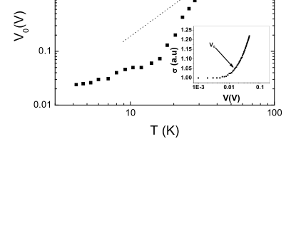
A similar conclusion can be derived from the temperature dependence of the current-voltage characteristics. It is useful to study conductivity versus voltage curves, , such as that shown in fig. 3 for an Au film. These curves are characterized by a voltage above which the conductivity increases with voltage thus deviating from ohmic behavior. Several theoretical works hill ; pollak ; shklovskii predict that non-Ohmic conductivity should occur for:
| (3) |
where F is the field applied across . Hence is expected to follow iv :
| (4) |
where m is between 1 and 2. The dependence of on T for a discontinuous Au film is shown in fig. 3. It is seen that for the I-V characteristic yields as expected. For there is a sharp drop in and a clear deviation from eq. 4. Such behavior could be interpreted as an unusually rapid increase in as the temperature is lowered below .
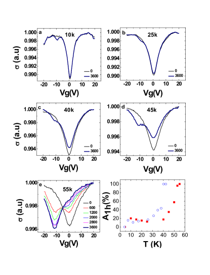
Perhaps the most remarkable phenomenon that occurs at low temperatures is a dramatic slowing down of the system’s electronic dynamics. Since the relaxation after any excitation follows an approximate logarithmic dependence it does not have a natural characteristic decay time. Nevertheless a number of methods have been proposed to experimentally define the ”slowness” of the relaxation in electron glasses zvi_tau , all giving equivalent characteristic times, . A popular method employs the ”two dip experiment” (TDE) ady2 . In this experiment the sample is allowed to equilibrate for a long time (of the order of a day) at a certain gate voltage . At this stage a fast scan yields a conductivity memory dip centered around . At time t=0 the gate voltage is abruptly changed to and fast scans are performed at selected time intervals. As a function of time the dip at is slowly suppressed while a new dip develops around . The characteristic relaxation time, , is defined as the time at which the amplitude of the two dips is equal.
A TDE for a discontinuous Au film sample at T=55K is shown in fig. 4e. It is seen that , which is a typical value for disordered samples having high carrier concentration zvi_dip . Upon lowering the temperature, all our films exhibits a huge increase in the characteristic relaxation time. For example, is found to be . This makes the systematic study of at different temperatures unpractical. Therefore we measure the fraction of relaxation that the system undergoes over a time of 1 hour. This is done in the following way: We allow the sample to equilibrate at relatively high T () while applying =0 for a time after which a dip is well developed. We then cool the sample to a different temperature, perform a gate voltage sweep to determine the size of the dip and change the gate voltage to . We then wait for one hour and measure the amplitude of the dip at . We define the amplitude ratio between the new dip and the old dip (at ) as . This is taken as a measure for the ”slowness” of the relaxation. The dependance of on temperature is shown in fig. 4. It is seen that there is a dramatic decrease of at . Similar behavior was obtained for all studied samples (over 12). The relaxation times and did not seem to depend on resistance but the amplitude of the memory dip decreased as the sample approached the metal-insulator transition.
Slowing down of relaxation processes with decreasing temperature may seem natural, however it is contrary to the situation in other electron glass systems. In amorphous and crystalline indium oxide zvi_T , and granular aluminum grenet2 the dynamics were found either to be independent on temperature or to slow down upon increasing T. The latter has been suggested as evidence that disordered electronic systems are quantum glasses zvi_T . In contrast, our Au films exhibit a dramatic slowing of the dynamics upon cooling. Furthermore, the temperature dependence of is very peculiar. Fig. 4f depicts (which inversely depends on ) as a function of T. It is seen that there is a sharp increase of relaxation times over a small temperature range.
The fact that the slowing down of the dynamics occurs at , where mesoscopic conductance fluctuations become significant, leads us to postulate that it is related to a significant dilution of the current carrying network (CCN). Note that, unlike in other electron glasses, the conductivity in the discontinuous films is strictly two dimensional. In addition, the SEM image of figure 1 shows that the grains are not closely packed, but rather the film morphology is composed of fractal shaped clusters connected by thin (single grain) bottlenecks rem . Hence this film is characterized by geometrical and not only electronic percolation which is typical of other hopping systems. At low temperatures many of these bottlenecks may disconnect from the CCN because of energy mismatches thus leaving most of the sample electrically cut-off. This gives rise to enhanced conductance fluctuations since the effective electronic system size is small. This also accounts for the apparent saturation of the R(T) curve at low T as shown in fig 1. Upon lowering T the electric current network becomes progressively dilute and the variable range hopping mechanism becomes less relevant as fewer sections of the sample dominate the conductivity. Eventually, at the extreme case where the conductivity governed by a single weak link it is expected to be temperature independent.
Under these conditions, at low T there is a very small probability for an electron to tunnel into and out of the current carrying network and most of the charge carriers are trapped in isolated regions of the sample. This causes a significant slowing down of the relaxation processes to equilibrium because these rely on many body hopping processes taking place in various parts of the sample. Since most of the sample is very weakly connected, the relaxation to equilibrium becomes extremely slow, thus hindering the development of a new MD at low temperatures. This can be realized from fig. 2b that shows the amplitude of the memory dip 20 minutes after the cool down, , as a function of temperature. It is seen that for this amplitude reduces with decreasing temperature. The amplitude of the memory dip in other electron glasses has shown to increase rapidly with decreasing temperature ady0 ; grenet2 . The decrease of with lowering temperature reflects the fact that the dynamics of the disconnected sections (most of the sample) have become extremely slow that the CCN is so dilute so that glassy properties are no longer relevant. Indeed some of the mesoscopic electron glasses studied in the past also did not exhibit a measurable MD vladimeso ; grenetmeso .
In conclusion we have shown that electron glasses based on 2D discontinuous films exhibit a sharp increase of relaxation times at low temperatures. These systems are characterized by a tenuous morphology which was not studied in the context of electron glasses so far. Our results demonstrate that relaxation to equilibrium hinges upon electronic transition in a wide region of the sample and when these become unavailable the relaxation processes are considerably impeded. The many-body and many-electron-hopping nature of the electron glass thus becomes strikingly apparent in these discontinuous films.
We are grateful for useful discussions with A. Amir, Z. Ovadyahu and M. Pollak. This research was supported by the Israeli academy of science (grant number 399/09)
References
- (1) M. Grunewald, B. Pohlman, L. Schweitzer, and D. Wurtz, J. Phys. C 15, L1153 (1982).
- (2) M. Pollak and M. Ortuno, Sol. Energy Mater. 8, 81 (1982);
- (3) M. Pollak, Philos. Mag. B 50, 265 (1984).
- (4) J. H. Davies, P. A. Lee and T. M. Rice, Phys. Rev. Lett. 49, 758 (1982).
- (5) G. Vignale, Phys. Rev. B 36, 8192 (1987).
- (6) C.J. Adkins, J.D. Benjamin, J.M.D. Thomas, J.W. Gardner, A.J.Mc Geown, . J. Phys. C 17, 4633 (1984).
- (7) M. Ben-Chorin, D. Kowal and Z. Ovadyahu, Phys. Rev. B44, 3420 (1991).
- (8) A. Vaknin, Z. Ovadyahu and M. Pollak, Europhys. Lett., 42 307 (1998)
- (9) A. Vaknin, Z. Ovadyahu and M. Pollak, Phys. Rev. Lett. 81, 669 (1998).
- (10) A. Vaknin, Z. Ovadyahu and M. Pollak, Phys. Rev. Lett. 84, 3402 (2000).
- (11) A. Vaknin, Z. Ovadyahu and M. Pollak, Phys. Rev. B65, 134208 (2002).
- (12) G. Martinez-Arizala, D.E. Grupp, C. Christiansen, A.M. Mack, N. Markovic, Y. Seguchi, A.M. Goldman, Phys. Rev. Lett. 78, 1130 (1997)
- (13) T. Grenet, Eur. Phys. J. B 32, 275 (2003).
- (14) Grenet et al., Eur. Phys. J. B 56, 183 (2007).
- (15) Z. Ovadyahu, Y.M. Xiong and P.W. Adams, Phys. Rev. B., 82, 195404, (2010)
- (16) Z. Ovadyahu, Phys. Rev. B 78, 195120 (2008).
- (17) M. Strongin, R. Thompson, O. Kammerer and J. Crow, Phys. Rev. B1, 1078 (1970).
- (18) A. Frydman and R.C. Dynes, Sol. State Comm. 110, 485 (1999).
- (19) A. Frydman, T.L. Kirk and R.C. Dynes, Solid State Commun. 114, 481 (2000).
- (20) A. L. Efros and B. I. Shklovskii, J. Phys. C 8, L49 (1975); B. I. Shklovskii and A. L. Efros, Electronic Properties of Doped Semiconductors (Springer, New York, 1984).
- (21) V. Orlyanchik and Z. Ovadyahu,Phys. Rev. B75, 174205 (2007).
- (22) J. Delahayea, T. Grenet, and F. Gay, Eur. Phys. J. B65, 5 (2008).
- (23) R. M. Hill, Philos. Mag. 24, 1307 (1971).
- (24) M. Pollak and I. Riess, J. Phys. C 9, 2339 (1976).
- (25) B. I. Shklovskii, Sov. Phys. Semicond. 10, 855 (1976)
- (26) D. Talukdar, U. N. Nandi, K. K. Bardhan, C. C. Bof Bufon, T. Heinzel, A. De, and C. D. Mukherjee, Phys. Rev. B84, 054205 (2011)
- (27) Z. Ovadyahu, Phys. Rev. B 73,214208 (2006).
- (28) T. Grenet and J. Delahaye, arXiv:1105.0984.
- (29) A. Amir, Y. Oreg and Y. Imry, Annual Review of Condensed Matter, 2, 235, (2011)
- (30) Z. Ovadyahu, Phys. Rev. Let. 99, 226603 (2007).
- (31) Though the morphology may change while heating the sample to room temperature we assume that the qualitative structure is similar at low T.