Ab-initio non-equilibrium quantum transport and forces with the real space projector augmented wave method
Resumé
We present an efficient implemention of a non-equilibrium Green function (NEGF) method for self-consistent calculations of electron transport and forces in nanostructured materials. The electronic structure is described at the level of density functional theory (DFT) using the projector augmented wave method (PAW) to describe the ionic cores and an atomic orbital basis set for the valence electrons. External bias and gate voltages are treated in a self-consistent manner and the Poisson equation with appropriate boundary conditions is solved in real space. Contour integration of the Green function and parallelization over k-points and real space makes the code highly efficient and applicable to systems containing several hundreds of atoms. The method is applied to a number of different systems demonstrating the effects of bias and gate voltages, multiterminal setups, non-equilibrium forces, and spin transport.
I Introduction
Electron transport across nanostructured interfaces is important in a range of different areas including nano-electronics, organic photovoltaics, and electrochemistry. First-principles modelling of electron transport at the nano-scale has so far mostly been applied to molecular junctions consisting of molecules contacted by metallic electrodesSmit et al. (2002); Djukic et al. (2005); Venkataraman et al. (2006); Quek et al. (2007); Li et al. (2007). However, more recent applications also include graphene nanoribbonsŞahin and Senger (2008); Novaes et al. (2010), semiconducting and metallic nanowiresMarkussen et al. (2010a); Lee et al. (2010); Ono and Hirose (2005), and bulk tunnelling junctions for magneto-resistance and electrochemical applicationsRungger et al. (2009); Chen et al. (2011). The rapid developments in these areas towards atomic-scale control of interface structures, and the continuing miniaturization of electronics components makes the development of efficient and flexible computational tools for the description of charge transport at the nano-scale an important endeavour.
The vast majority of first-principles electron transport studies have been based on density functional theory (DFT) within the local density (LDA) or generalized gradient (GGA) approximations. This approach is in principle unjustified because the eigenvalues of the effective Kohn-Sham Hamiltonian do not represent the true quasiparticle energy levels. In particular, for tunneling junctions the energy gap between the highest occupied states and lowest unoccupied states is too smallDell’Angela et al. (2010); Garcia-Lastra et al. (2009) and this can lead to an overestimation of the conductance. More accurate calculations incuding self-interaction correctionsToher and Sanvito (2007) and more recently the many-body GW approximationStrange et al. (2011); Strange and Thygesen (2011); Rangel et al. (2011) yield conductance values in better agreement with experiments. On the other hand, the NEGF-DFT approach often provides a satisfactory qualitative descriptionHybertsen et al. (2008); Li et al. (2007) and its computational simplicity makes it a powerful tool for addressing non-equilibrium properties of complex systems. It should be mentioned that the formal problems associated with the use of DFT for transport are overcome by time-dependent DFT (TDDFT) which allows for an, in principle, exact description of the (longitudinal) current due to an externally applied fieldStefanucci and Almbladh (2004). However, it has been recently found that the standard TDDFT exchange-correlation potentials do not yield any improvement over the NEGF-DFT in terms of accuracy in predicting conductanceYam et al. (2011).
In addition to the electronic current it is of interest to model the forces acting on the atoms under non-equilibrium conditions, i.e. under a finite bias voltage. Such forces ultimately determine the stability of current carrying molecular devicesDundas et al. (2009); Lü et al. (2010), but can also be exploited to deliberately control the motion of single molecules by e.g. injecting electrons into the molcular orbitals using a scanning tunneling microscope (STM).
In this paper we describe the implementation of the NEGF-DFT method in the GPAWEnkovaara et al. (2010); Larsen et al. (2009) electronic structure code. In GPAW the electronic states can be described either on a real space grid or using an atomic orbital basis set. For the NEGF calculations, the Green function is expanded in the atomic orbital basis while the Poisson equation is solved in real space. Contour integration and sparse matrix techniques together with parallelization over both k-points and real space is exploited for optimal efficiency. Although the basic elements of our implementation are not new and have been described in earlier papersTaylor et al. (2001a); Brandbyge et al. (2002); Xue et al. (2002), the possibility of applying a general gate and/or finite bias voltage, the use of multiple leads, and inclusion of non-equilibrium forces on the ions provides a flexible and efficient computational platform for general purpose modelling of charge transport at the nano-scale and should be of interest to a large and growing community.
This paper is organized as follows. In Section 2 the transport model and formalism are introduced. In Section 3 we describe the complex contour integration technique used to obtain the non-equilibrium electron density from the Green function. Section 4 describes the use of sparse matrix methods, and in Section 5 we discuss the real space solution of the Poisson equation. A number of illustrative applications are presented in Section 7.
II Method
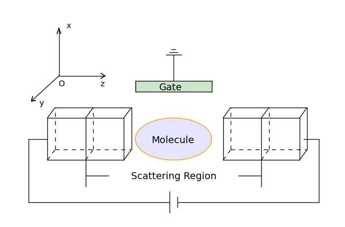
The transport model is shown in Fig. 1. Following the standard approach, the system is divided into left and right electrodes and the central scattering region (see the detailed description in the caption). The Hamiltonian of the system is given by (all notation related to PAW methodology is consistent with earlier GPAW papersEnkovaara et al. (2010); Larsen et al. (2009))
| (1) |
where denote the atoms in the system and label the PAW projector functions of a given atom. Using a (non-orthogonal) atomic orbital basis set, the Hamiltonian can be written in the following generic form
| (2) |
The “on-site” Hamiltonian matrices of the electrodes, (left) and (right), and the coupling matrices and , can be obtained from a homogeneous bulk calculation. If a bias voltage is applied, the matrices corresponding to the left and right electrodes should be shifted by relative to each other, e.g. and , where denotes the overlap matrix. We assume that there is no coupling between basis functions belonging to different electrodes. This assumption can be always satisfied by making the scattering region large enough.
The retarded Green function is written as
| (3) |
The self-energies, , represent the coupling to the electrodes and are obtained using the efficient decimation technique Guinea et al. (1983).
The lesser Green function is written asjauho
| (4) |
The latter term is nonzero for truly bound states and vanishes for states acquiring any width.
The pseudo density matrix (for the pseudo wave in the PAW framework) is the integral of
| (5) | |||||
Here and is a contour for the integral to be discussed more in Sec. 3.
The non-equilibrium electron density is obtained as
| (6) |
where is an atomic orbital basis function and is the atomic pseudo core density. As is standard in the PAW formalism a tilde indicates a smooth quantity as opposed to an all electron quantity. The smooth charge density is given by
| (7) |
where are multipole moments and is a so-called shape function. The last term is the contribution to the charge density coming from the positively charged nuclei.
The effective potential is found as
| (8) |
where the Coulomb potential satisfies the Poisson equation , while and are the exchange-correlation potential and zero-potential, respectively. is a parameter chosen to smoothen and which vanishes outside the augmentation sphere of atom Kiejna et al. (2006).
To obtain self-consistency we thus have the iteration process . After convergence the current can be calculated by
| (9) |
where . For a derivation of the current formula we refer the reader to Ref. Meir and Wingreen (1992) (orthogonal basis) or Ref. Thygesen (2006) (non-orthogonal basis).
The non-equilibrium force is obtained from the derivative of the total energy with respect to atomic positions. In the PAW framework, the total energy is written
| (10) |
with
The force can be obtained as
| (11) |
where
| (12) | |||||
We note that the expression given above does not include the recently discussed Berry phase contributions to the nonequilibrium forceLü et al. (2010).
III Numerical details
III.1 Contour integration technique
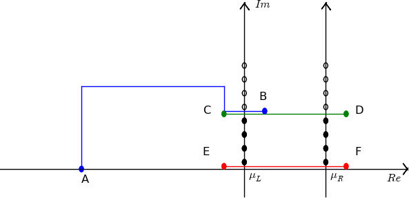
The contour for the Green function integral in Eq. (5) is shown in Fig. 2. The retarded and lesser Green functions are integrated along the path AB (see Fig. 2) in the upper half plane and the path EF closely above the real axis in the bias windowBrandbyge et al. (2002); Taylor et al. (2001b).
For the retarded Green function we use Gaussian quadrature by which a precision corresponding to a order polynomial can be obtained by points. We use an adaptive method to find the energy points necessary to obtain a sufficient precisionLi (2008): for a given region , the integral of a function can be estimated with the Gauss-Lobatto formula,
| (13) |
and furthermore a Kronrod formula can be used to estimate the precision of the integralPatterson (1968)
| (14) | |||||
The difference between and can be taken as the precision of the integral.
The adaptive procedure to get the integral of the Green function in a region is
-
1.
calculate and , then compare the difference with the tolerance .
-
2.
if is smaller than , the integral is converged and is used as integral result. If not, divide the region into three subregions and redo the step 1 for each subregion until the integral is converged in the whole region.
For the lesser Green function inside the bias window, we use the simple composite trapezoidal rule to obtain the integral. However, numerical errors can easily occur close to the real axis where the Green function has singularities. For this reason we apply the double contour method introduced in Ref. Brandbyge et al., 2002: First, the integral of the retarded Green function is calculated along the path CD (Fig. 2) above the bias window, which is the spectrum for all the electronic states in the bias window , then both electron spectrum and hole spectrum are integrated along the path EF, and we have according to the definition of the Green function, where electron density and hole density are obtained from the integral of and respectively. The numeric error, is normally a non-zero quantity due to the integral insufficiency. As a correction, the error is distributed to and by the matrix element weight.
III.2 Sparse matrix handling
Because the matrix inversion cost scales as , where is the dimension of the matrix, the matrix inversion turns out to be the main computational cost for large systems. Hence a sparse matrix method is implemented to obtain the Green function.
We define a quenching layer as a slab whose left side has no overlap with the right side due to the finite cutoff in the range of the atomic orbitals. Hence an overlap or Hamiltonian matrix can be split into several blocks, with each block representing the onsite values of a quenching layer or the coupling between two adjacent quenching layers. Note that quenching layers here are different from principal layers used in the transport framework, where the latter is supposed to be repeatable as well.
Physical quantities like density or transmission is often determined by fairly few blocks of a matrix. To see this consider the simple example of a two-probe system. In this case, the scattering region is divided into 5 quenching layers. Fig. 3 shows the sparse matrix structure of the overlap or the Hamiltonian matrix. The blocks outside the scattering region are from electrode calculations and always fixed.
First we discuss how to obtain the real-space pseudo-density which can be obtained by a projection of the pseudo-density matrix as in Eq. 6. We see that if the states and have no overlap, the contribution from the pseudo-density matrix is zero, i.e., the white blocks in Fig. 3a do not affect the density. So when we calculate the density matrix from the integral of the Green’ function, only the blue and green blocks in the Green function matrix (Fig. 3a) are necessary. There are really two different parts, because two types of Green functions are involved when calculating the density matrix: the equilibrium part and the non-equilibrium part. We need the blue and green blocks of the retarded Green function for the former and of the Keldysh Green function for the latter. Through Eq. 4 and the finite extent of the self-energy matrix, which is only non-zero in the principle layers close to the electrodes, we see that the blue and green blocks in Fig. 3 in the Keldysh Green function matrix can be obtained from only the red blocks of the retarded Green function (Fig. 3c). So when we do the matrix inversion to calculate the retarded Green function by Eq. 3, the red blocks in Fig. 3a are necessary for energy points on the path EF in Fig. 2, and the blue and green blocks in Fig. 3c are necessary for energy points on the other path segments in Fig. 2.
We can also see that the red and orange blocks in Fig. 3b are needed to calculate the density of states () by and the pink blocks in Fig. 3b are needed to calculate the transmission function .
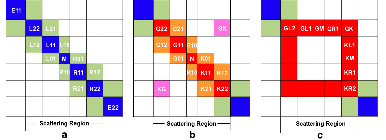
The formulas below provide a quick solution for the necessary blocks. Here we just consider this particular matrix(shown in Fig. 3) as an example to show how the method works. A general formalism, which works for arbitrary number of electrodes and arbitrary number of principal layers in each electrode, is introduced in Ref. Zekan et al., 2008.
First, the central block in Fig. 3b of the retarded Green function can be solved through the equations
| (15) | |||||
| (16) | |||||
| (17) |
where and are the blocks shown in Fig. 3a representing the matrix . Then, for the remaining blocks of the retarded Green function matrix, we have to iterate the formulas
| (18) |
where is the block from the central part to electrode L and is in Eq. 18, the blocks from the central part to electrode R have a similar solution. For all the required blocks, a quick solution can be obtained using a combination of the recursive formulas Eq. 18. If we denote the number of quenching layers by , the computational cost is roughly given by times the cost of an inversion operation plus 4 times the cost of matrix multiplicationZekan et al. (2008).
III.3 Fixed boundary conditions
The electronic potential of the metal electrodes will usually be very efficiently screened so that after only a few atomic layers into the electrodes we can assume that the potential is equal to the equilibrium potential plus/minus a possible constant bias potential. We shall apply open boundary conditions (in contrast to, say, periodic ones) where the bias is applied by fixing the potential values at the boundaries before solving the Poisson equationOzaki et al. (2010). This procedure also allows for a net charge in the scattering region in which case the perturbation of the electron potential into the electrodes will of course be somewhat more long ranged.
The Poisson equation is solved in reciprocal space in the and directions while it is solved in real space in the -coordinate, i.e., in the the transport direction. Mathematically we have
| (19) |
where is the vectors of the 2-d real grids used for the Fourier transformation.
Eq. 19 is solved by the sparse matrix linear equation subroutine provided by the Lapack package. An advantage of this Poisson equation solution is the good parallelization behavior. The 2-d Fourier transformations are independent for the different real-space slices, and the linear equations Eq. 19 can be solved independently for different -vectors.
IV Results
IV.1 Quantum capacitor
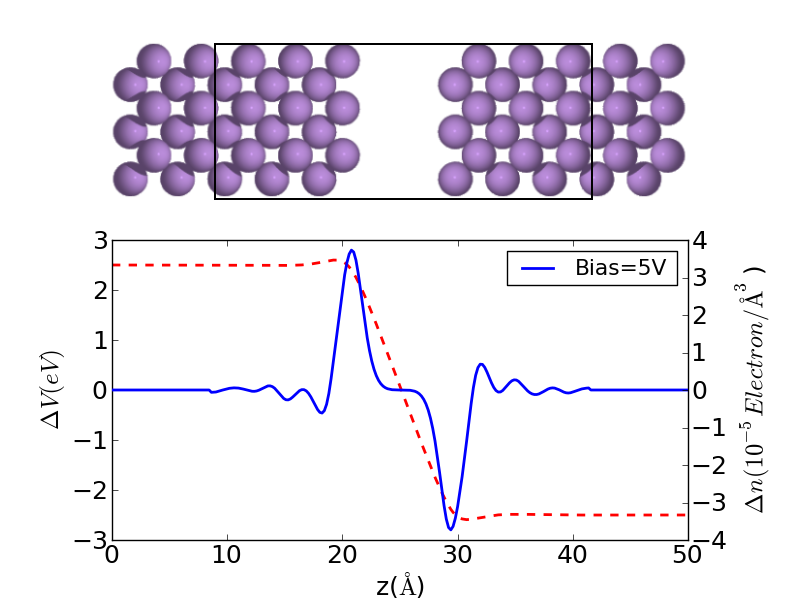
We consider a simple capacitor system consisting of two semi-infinite Na electrodes separated by a vacuum gap, see upper part of Fig. 4. When a bias voltage is applied to the system, electrons accumulate/deplete on the Na(100) surfaces. According to the classic parallel plate capacitor model, the surface charge should be
| (20) |
where , , are the vacuum permittivity, area cross section of the unit cell, and the gap distance, respectively. We integrate the induced charge density in real space and obtain the net charge accumulation , which is close to the result of classic theory . One difference is that in the quantum theory, the charge decays from the surface into the bulk in an oscillatory fashion (Friedel oscillations), instead of being localized exactly on the surface as assumed in the classic model. We also note that at a distance of about 4 layers from the surface the values for both the potential and the charge are very close to their bulk values. Hence this calculation confirms the screening approximation, namely that a few layers away from the surface or scattering region the potential has reached its bulk value. Finally, we note that the relatively high bias voltage of is possible in the present case where no current is flowing. On the other hand, the non-equilibrium states determining the current flow become increasingly difficult to calculate accurately for larger bias values due to the insufficient integral of the Keldysh Green function in the bias window. As a consequence electron transport calculations are typically possible/reliable up to bias voltages of around V, depending on the transparency of the junction.
IV.2 Non-equilibrium forces
The calculation of non-equilibrium forces is in principle a delicate problem involving non-conservative componentsDi Ventra et al. (2004); Lü et al. (2010); Dundas et al. (2009). For highly conducting molecular bridges an instability may occur which involves the Berry phase of the wave function. The description of such phenomena is beyond the scope of the usual NEGF+DFT framework, but in simpler cases, in particular in cases with no or little current flow, the force expressions Eqs. 11-12 still apply.
As an example, we show here a non-equilibrium force calculation for a Au/N2/Au junction, where we can see the tendency towards molecular dissociation under a bias voltage. The structure (see upper part of Fig. 5) is relaxed under zero bias until the maximum force is below 0.01eV/Å. When a positive bias is applied, electrons are redistributed over the molecule due to the electric field. Consequently, the two nitrogen atoms start to repel each other due to increased Coulomb repulsion which weakens the bond. The actual quantity of charge transfer to the molecule, which is about 0.01e for 1V bias voltage on this system, shifts up the molecular energy spectrum, i.e. the energy levels follow the chemical potential of the left electrode (see Fig. 5 middle panel). The force is mainly occurring only between the two nitrogen atoms, while there is no force induced between the electrode atoms and the N2 molecule. Equivalently, a negative bias voltage shifts down the levels and pull electrons out of the N2 molecule, and leads to an attractive force between the two nitrogen atoms.

IV.3 Electrostatic gate control
One way of controlling the current flow through a nano-scale conductor is by electrostatic gating. This has been demonstrated experimentally for graphene, where a metal-insulator transition was induced by gatingB.Oostinga et al. (2008); M.F.Craciun et al. (2009), and for single-molecule junctions where the individual electronic levels were moved in energy relative to the Fermi level of the source/drain electrodesKubatkin et al. (2003); Hyunwook et al. (2009). At the single molecule scale, the gate-molecule coupling is to a large extent determined by the device geometry with the screening effect playing an important roleDatta et al. (2009). For numerical simulations, the typical method of applying a gate is to add an external potential to the effective potential of the system
| (21) |
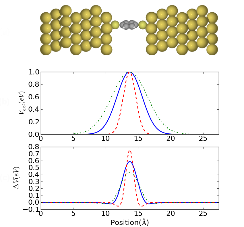
We now consider the prototypical Au-BDT-Au junction (see upper panel of Fig. 6) subject to three different gate potentials, (see middle panel of Fig. 6). We note that the structure of the Au/BDT junction is presently being debatedStrange et al. (2010); Jadzinsky et al. (2007); Wang et al. (2009). However, for our purpose the simple model makes the sense.
In the lower part of Fig. 6 we plot the resulting effective gate potential where the subscript denotes self-consistency, and the superscript denotes zero gate voltage. Due to the screening in the metal, the effective gate potentials only affect the molecule region, and the narrower gate potential is seen to be less influenced by the self-consistency because it does not induce considerable charge transfer at the metal surfaces - a charge transfer that otherwise tends to reduce the gate effect on the molecule. We note that the gate efficiency factor, , for these three potentials are about 0.8, 0.6, and 0.4 in the molecular region with the larger efficiency obtained for the more localized gate potential. The value of 0.4 obtained for the most delocalized potential is fairly close to an experimental studyHyunwook et al. (2009) of the Au-BDT-Au system where an efficiency factor of 0.25 was reported.
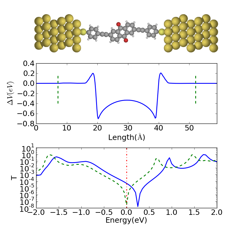
In the following we illustrate how the gate voltage can be used to tune the conductance of a molecular junction. It has recently been shown that the transport through the molecule anthraquinone is strongly suppressed due to destructive quantum interference occurring close to the Fermi level when the molecule is connected to metallic electrodesMarkussen et al. (2010b, c). The quantum interference leads to a dip in the transmission function inside the energy gap between the highest occupied (HOMO) and lowest unoccupied (LUMO) molecular orbitals. Hence a large on-off ratio is expected when shifting the molecular energy levels by an external gate voltage. The upper panel of Fig. 7 shows the molecule connected to two gold fcc(111) surfaces through Au-S bonds. The effective potential with the gate voltage -2V is shown in the middle panel. We see that the potential of the central part of the anthraquinone molecule is shifted less than the potential for the outer parts of the molecule. This is due to the fact that different parts of the molecule polarize differently as a consequence of the detailed electronic structure. The HOMO is for example mainly localized at the connecting wires. The lower panel of Fig. 7 shows the change of transmission coefficient when a gate voltage of -2V is applied. Due to the characteristic interference dip in the transmission a large on-off ratio of about a factor of 1000 is achieved. Note that the relatively poor gate efficiency of around 0.1 is due to Fermi level pining of the HOMO.
IV.4 Spin transport
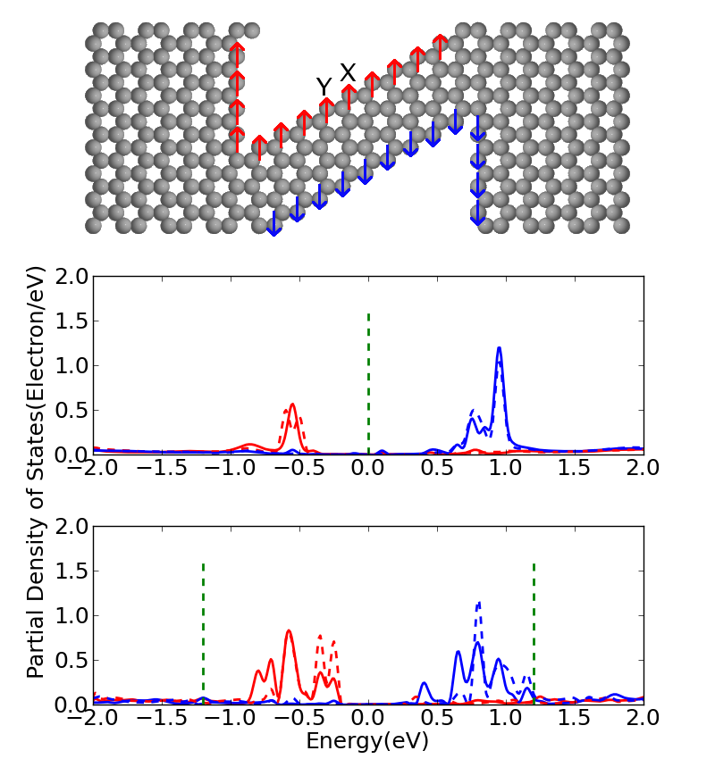
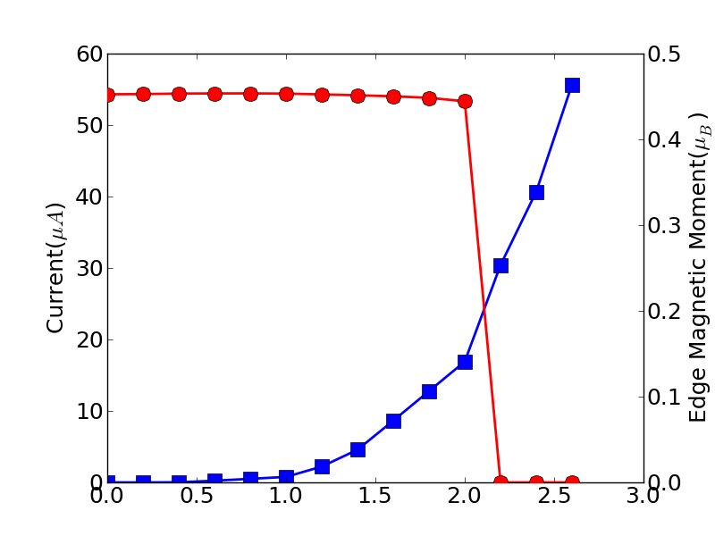
In this section, we investigate the nonequilibrium-driven magnetic transition in the spin transport in zigzag graphene nanoribbon(ZGNR) which is proposed in Ref.Areshkin and Nikolić (2009) based on tight-binding calculations. The ZGNR’s edge is spin-polarized and it has an anti-ferromagnetic spin configuration if its number of atomic layers is evenFujita et al. (1996). A gap about 1eV is opened between the different spin states and makes the ZGNR a semiconductor. It was noticed by Denis et al. that the ZGNR’s magnetic ordering is killed when the external bias voltage exceeds the size of the gapAreshkin and Nikolić (2009). Here we reproduce this result for the graphene/ZGNR/graphene system shown in the upper panel of Fig. 8, where a ZGNR(nn=8) is sandwiched between two semi-infinite graphene flakes. Under zero bias the of the central C atom along the ZGNR edge shows two peaks above and below the Fermi level, corresponding to the different spin directions (middle panel in Fig. 8). The distance between the two peaks is about , and equals the band gap. When this bias voltage reaches , the current starts to increase, see Fig. 9. At bias voltages the edge magnetic moment disappears very abruptly, and the current starts to increase even faster.
Interestingly, in the tight-binding calculations presented in Ref. Areshkin and Nikolić (2009), both the magnetic moment and the current show a very abrupt feature at the bias threshold, while in our calculation, the current increases rather smoothly. This can be explained by the non-equilibrium potential in the ab-initio calculation leads to a rehybridization and broadening of the spectral peaks, see lower panel of Fig. 8. We also note that in our calculation the disappearance of the magnetic moment is due to the two Stoner peaks moving into the bias window being half-occupied, different from the complete band collapse in the Ref. Areshkin and Nikolić (2009),this is because our ZGNR is not long enough. We can see from the lower panel of Fig. 8 the gap shrinks more for the C atom further from the contact.
IV.5 Multi-terminal transport
The expression for the Green function of the scattering region Eq. (3) can be straightforwardly extended to a multi-terminal situation
| (22) |
where is the index of the terminals. In contrast to the situation for a two-probe calculation, a zero boundary condition is applied for the effective potential for a multi-terminal system, and buffer atoms are used to represent semi-infinite leads. This approach to multiterminal transport has been previously investigated in Ref. Zhang et al., 2005. It should be noted that the self-energy of a lead has to be “rotated” by an orthogonal transformation when the lead is not along either the , or axes.
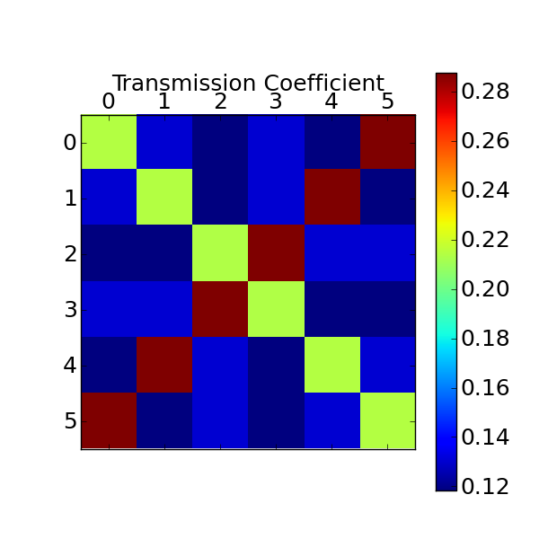
As an example, we consider a C60 molecule connected to six linear carbon atomic chains. Fig. 10(left) shows the projected in real space evaluated at the Fermi level. The coverage suggests the scattering states are itinerant in the whole system and the contact between the carbon chain and the C60 moelcule is transparent. Fig. 10(right) shows a 2D averaged potential in a plane cutting through the C60 molecule.

A matrix indicating the transmission at the Fermi level between the different leads is shown in the Fig. 11. The matrix index notation represents the lead number as shown in Fig. 10(left). In particular, the diagonal corresponds to back scattering, i.e. it gives the reflection probability. We can see that electrons are more easily transmitted between leads opposing each other, whereas the transmission decreases if the electron has to turn an angle during the scattering process. This intuitive phenomenon can be explained by the quantum interference of the different partial waves. For the straightforward scattering, the quantum phases are the same for all the paths passing through the C60 molecule, and the electron therefore attains the greatest transmission probabilityMarkussen et al. (2010c).
V Computational details
For completeness we list the key input parameters and CPU timings for the examples presented in this paper in the table below.
| System | K-sampling | Functional | Basis | Lead K-sampling | processor number | walltime(hour) |
| Capacitor | (4,4) | LDA | SZ | (4,4,15) | 4 | 0.5 |
| Au/N2/Au | (2,2) | PBE | DZP(SZP) | (2,2,15) | 32 | 3 |
| Gate(BDT) | (2,2) | PBE | DZP(SZP) | (2,2,15) | 32 | 6 |
| Gate(anthraquinon) | (2,2) | PBE | DZP(SZP) | (2,2,15) | 32 | 8 |
| Graphene/ZGNR/Graphene | (2,1) | PBE | SZP | (2,2,7) | 32 | 6 |
| C60 | (1,1) | LDA | SZ | (1,1,15) | 32 | 2 |
VI Summary
We have described the implementation of the NFGF+DFT transport method in the GPAW code and illustrated its performance through application to a number of different molecular junctions. The electronic structure is described within the PAW methodology which provides all-electron accuracy at a computational cost corresponding to pseudopotential calculations. The Green functions are represented in a basis set consisting of atomic-like orbitals while the Poisson equation with appropriate boundary conditions is solved in real space. The code is parallelized over k-points and real space domains and sparse matrix techniques are applied for maximal efficiency. The flexibility of the method was illustrated through examples demonstrating electron transport under finite bias voltage, effect of electrostatic gating, spin transport, nonequilibrium forces, and multi-terminal leads.
VII Acknowledgment
The authors thank Jens Jørgen Mortensen and Ask Hjorth Larsen for helpful discussions. The authors acknowledge support from the Danish Center for Scientific Computing through grant HDW-1103-06. The Center for Atomic-scale Materials Design is sponsored by the Lundbeck Foundation.
Litteratur
- Smit et al. (2002) R. H. M. Smit, Y. Noat, C. Untiedt, N. D. Lang, M. C. van Hemert, and J. M. van Ruitenbeek, Nature, 419, 906 (2002).
- Djukic et al. (2005) D. Djukic, K. S. Thygesen, C. Untiedt, R. H. M. Smit, K. W. Jacobsen, and J. M. van Ruitenbeek, Phys. Rev. B 71, 161402 (2005).
- Venkataraman et al. (2006) L. Venkataraman, J. E. Klare, I. W. Tam, C. Nuckolls, M. S. Hybertsen, and M. L. Steigerwald, Nano Lett. 6, 458 (2006).
- Quek et al. (2007) S. Y. Quek, L. Venkataraman, H. J. Choi, S. G. Louie, M. S. Hybertsen, and J. B. Neaton, Nano Lett. 7, 3477 (2007).
- Li et al. (2007) C. Li, I. Pobelov, T. Wandlowski, A. Bagrets, A. Arnold, and F. Evers, J. Am. Chem. Soc. 130, 318 (2007).
- Şahin and Senger (2008) H. Şahin and R. T. Senger, Phys. Rev. B 78, 205423 (2008).
- Novaes et al. (2010) F. D. Novaes, R. Rurali, and P. Ordejón, ACS Nano 4, 7596 (2010).
- Markussen et al. (2010a) T. Markussen, R. Rurali, X. Cartoixà, A.-P. Jauho, and M. Brandbyge, Phys. Rev. B 81, 125307 (2010a).
- Lee et al. (2010) Y. Lee, K. Kakushima, K. Shiraishi, K. Natori, and H. Iwai, Journal of Applied Physics 107, 113705 (2010).
- Ono and Hirose (2005) T. Ono and K. Hirose, Phys. Rev. Lett. 94, 206806 (2005).
- Rungger et al. (2009) I. Rungger, O. Mryasov, and S. Sanvito, Phys. Rev. B 79, 094414 (2009).
- Chen et al. (2011) J. Chen, J. S. Hummelshøj, K. S. Thygesen, J. S. Myrdal, J. K. Nørskov, and T. Vegge, Catalysis Today 165, 2 (2011).
- Dell’Angela et al. (2010) M. Dell’Angela, G. Kladnik, A. Cossaro, A. Verdini, M. Kamenetska, I. Tamblyn, S. Y. Quek, J. B. Neaton, D. Cvetko, A. Morgante, et al., Nano Lett. 10, 2470 (2010).
- Garcia-Lastra et al. (2009) J. M. Garcia-Lastra, C. Rostgaard, A. Rubio, and K. S. Thygesen, Phys. Rev. B 80, 245427 (2009).
- Toher and Sanvito (2007) C. Toher and S. Sanvito, Phys. Rev. Lett. 99, 056801 (2007).
- Strange et al. (2011) M. Strange, C. Rostgaard, H. Häkkinen, and K. S. Thygesen, Phys. Rev. B 83, 115108 (2011).
- Strange and Thygesen (2011) M. Strange and K. S. Thygesen, Beilstein Journal of Nanotechnology 2, 746 (2011).
- Rangel et al. (2011) T. Rangel, A. Ferretti, P. E. Trevisanutto, V. Olevano, and G.-M. Rignanese, Phys. Rev. B 84, 045426 (2011).
- Hybertsen et al. (2008) M. S. Hybertsen, L. Venkataraman, J. E. Klare, A. C. Whalley, M. L. Steigerwald, and C. Nuckolls, Journal of Physics: Condensed Matter 20, 374115 (2008).
- Stefanucci and Almbladh (2004) G. Stefanucci and C. O. Almbladh, Europhys. Lett.,67, 14(2004).
- Yam et al. (2011) C. Y. Yam, X. Zheng, G. H. Chen, Y. Wang, T. Frauenheim, and T. A. Niehaus, Phys. Rev. B 83, 245448 (2011).
- Dundas et al. (2009) D. Dundas, E. J. McEniry, and T. T. N., Nat. Nanotechnol., 4, 99(2009).
- Lü et al. (2010) J.-T. Lü, M. Brandbyge, and P. Hedegård, Nano Lett. 10, 1657 (2010).
- Enkovaara et al. (2010) J. Enkovaara, C. Rostgaard, J. J. Mortensen, J. Chen, M. Dułak, L. Ferrighi, J. Gavnholt, C. Glinsvad, V. Haikola, H. A. Hansen, et al., Journal of Physics: Condensed Matter 22, 253202 (2010).
- Larsen et al. (2009) A. H. Larsen, M. Vanin, J. J. Mortensen, K. S. Thygesen, and K. W. Jacobsen, Phys. Rev. B 80, 195112 (2009).
- Taylor et al. (2001a) J. Taylor, H. Guo, and J. Wang, Phys. Rev. B 63, 245407 (2001a).
- Brandbyge et al. (2002) M. Brandbyge, J.-L. Mozos, P. Ordejón, J. Taylor, and K. Stokbro, Phys. Rev. B 65, 165401 (2002).
- Xue et al. (2002) Y. Xue, S. Datta, and M. A. Ratner, Chemical Physics 281, 151 (2002).
- Guinea et al. (1983) F. Guinea, C. Tejedor, F. Flores, and E. Louis, Phys. Rev. B 28, 4397 (1983).
- (30) See, for example, H. Haug and A.-P. Jauho, Quantum Kinetics in Transport and Optics of Semiconductors (Springer-Verlag, New York, 1998).
- Kiejna et al. (2006) A. Kiejna, G. Kresse, J. Rogal, A. De Sarkar, K. Reuter, and M. Scheffler, Phys. Rev. B 73, 035404 (2006).
- Meir and Wingreen (1992) Y. Meir and N. S. Wingreen, Phys. Rev. Lett. 68, 2512 (1992).
- Thygesen (2006) K. S. Thygesen, Phys. Rev. B 73, 035309 (2006).
- Taylor et al. (2001b) J. Taylor, H. Guo, and J. Wang, Phys. Rev. B 63, 245407 (2001b).
- Li (2008) R. Li, Phd Thesis, School of Electronics and Computer Science, Peking University (2008).
- Patterson (1968) T. N. L. Patterson, Math. Comput. 22, 847 (1968).
- Zekan et al. (2008) Q. Zekan, H. Shimin, L. Rui, S. Ziyong, Z. Xingyu, and X. Zengquan, J. Comput. Theor. Nanosci. 5, 671 (2008).
- Ozaki et al. (2010) T. Ozaki, K. Nishio, and H. Kino, Phys. Rev. B 81, 035116 (2010).
- Di Ventra et al. (2004) M. Di Ventra, Y.-C. Chen, and T. N. Todorov, Phys. Rev. Lett. 92, 176803 (2004).
- B.Oostinga et al. (2008) J. B.Oostinga, H. B.Heersche, X. Liu, A. F.Morpurgo, and L. M.K.Vandersypen, Nature Mater.,7, 151 (2008).
- M.F.Craciun et al. (2009) M.F.Craciun, S.Russo, M.Yamamoto, J. B.Oostinga, A. F.Morpurgo, and S.Tarucha, Nat. Nanotechnol., 4,383 (2009).
- Kubatkin et al. (2003) S. Kubatkin, A. Danilov, M. Hjort, J. Cornil, J.-L. Bredas, N. Stuhr-Hansen, P. Hedegard, and T. Bjornholm, Nature,425,698 (2003).
- Hyunwook et al. (2009) S. Hyunwook, K. Youngsang, J. Y. Hee, J. Heejun, R. M. A., and L. Takhee, Nature,462, 1039 (2009).
- Datta et al. (2009) S. S. Datta, D. R. Strachan,and A. T. Charlie Johnson, Phys. Rev. B 79, 205404 (2009).
- Strange et al. (2010) M. Strange, O. Lopez-Acevedo, and H. Häkkinen, J. Phys. Chem. Lett. 1, 1528 (2010).
- Jadzinsky et al. (2007) P. D. Jadzinsky, G. Calero, C. J. Ackerson, D. A. Bushnell, and R. D. Kornberg, Science 318, 430 (2007).
- Wang et al. (2009) Y. Wang, Q. Chi, N. S. Hush, J. R. Reimers, J. Zhang, and J. Ulstrup, J. Phys. Chem. C 113, 19601 (2009).
- Markussen et al. (2010b) T. Markussen, J. Schiotz, and K. S. Thygesen, The Journal of Chemical Physics 132, 224104(2010b).
- Markussen et al. (2010c) T. Markussen, R. Stadler, and K. S. Thygesen, Nano Lett. 10, 4260 (2010c).
- Areshkin and Nikolić (2009) D. A. Areshkin and B. K. Nikolić, Phys. Rev. B 79, 205430 (2009).
- Fujita et al. (1996) M. Fujita, K. Wakabayashi, K. Nakada, and K. Kusakabe, Journal of the Physical Society of Japan 65, 1920 (1996).
- Zhang et al. (2005) J. Zhang, S. Hou, R. Li, Z. Qian, R. Han, Z. Shen, X. Zhao, and Z. Xue, Nanotechnology 16, 3057 (2005).