Localization of superconductivity in superconductor-electromagnet hybrids
Abstract
We investigate the nucleation of superconductivity in a superconducting Al strip under the influence of the magnetic field generated by a current-carrying Nb wire, perpendicularly oriented and located underneath the strip. The inhomogeneous magnetic field, induced by the Nb wire, produces a spatial modulation of the critical temperature , leading to a controllable localization of the superconducting order parameter (OP) wave function. We demonstrate that close to the phase boundary the localized OP solution can be displaced reversibly by either applying an external perpendicular magnetic field or by changing the amplitude of the inhomogeneous field.
pacs:
74.25.Dw, 74.25.Op, 74.78.Na, 74.78.-wThe sensitivity of superconductivity to the local strength of a magnetic field has been exploited during the last years to confine superconductivity by applying a non-uniform magnetic field [1, 2, 3]. The experimental realization of this “magnetic” confinement can be achieved, e.g., in hybrid superconductor (S) – ferromagnet (F) structures and ferromagnetic superconductors. The properties of the ferromagnetic superconductors and the S/F hybrids with rather strong exchange interaction between superconducting and ferromagnetic subsystems were discussed in the reviews [4, 5, 6, 7]. Hereafter we will focus on the flux-coupled hybrids, where the interaction between superconducting element and the sources of the magnetic field (e.g., domain walls in the ferromagnetic film) occurs via slowly decaying stray fields only [8, 9, 10].
In general, for thin-film superconducting samples, infinite in the lateral directions, superconducting order parameter (OP) wave function first nucleates near the minima, where is the out-of-plane component of the total magnetic field, is the applied external magnetic field (see arguments, e.g., in [10]). Depending on , favorable conditions for the appearance of superconductivity can be fulfilled either above domain walls in a thick ferromagnetic substrate (domain–wall superconductivity [11, 12, 13]), or above magnetic domains of opposite polarity with respect to the sign (reverse-domain superconductivity [14, 15, 16, 17, 18]). The external-field-induced crossover between domain–wall superconductivity and reverse-domain superconductivity as increases can result in an unusual dependence of the superconducting critical temperature on , which can be nonlinear or even non-monotonous [18, 19, 20, 21] in contrast to a plain superconducting film in a uniform magnetic field. In addition, these domain patterns are periodic in space and therefore superconductivity has to be located at all magnetically compensated areas. In order to have a singly connected OP solution a non-periodic field profile is needed [22]. It is interesting to note that the stray field of a single domain wall in a thin ferromagnetic layer cannot provide domain-wall superconductivity and non-monotonous (or, in the other words, reentrant) phase boundary due to vanishing of the field at large distances from the domain wall [2]. Even if the amplitude of the stray field produced by domain structure becomes insufficient to localize superconductivity, such parallel magnetic domains can induce preferential vortex motion and giant anisotropy of the critical currents in superconducting films and crystals [23, 24, 25, 26, 27, 28].
We would like to note that the amplitude of the stray magnetic field and its profile in real S/F bilayers are dictated by the saturated magnetization of the ferromagnet and by the period of the domain structure (or magnetic dot array), therefore the flexibility of S/F hybrids is limited [3, 20, 29, 30, 31]. Full control over the amplitude of the inhomogeneous magnetic field can be reached for the hybrid structures, where the ferromagnetic subsystem is replaced by current-carrying coils/wires. Such superconductor-electromagnet (S/Em) hybrid systems (also called cryotrons) were invented in 1950’s and originally considered as superconducting computer elements and circuits controlled by local magnetic field of the coils/wires (see classical textbooks and reviews [32, 33, 34, 35]). However the most transport measurements done on cryotrons were carried out at low temperatures, when the ability to manipulate the intensive superconducting currents seems to be the most effective. To the best of our knowledge the report of the S/Em properties at high temperatures was carried out by Pannetier et al. [36]. In this work for the S/Em system, consisting of a plain Al film and a lithographically defined array of parallel metallic lines, it was experimentally demonstrated that (i) the dependence can be non-monotonous for considerably large driving current in these metallic lines and (ii) the shape of the can be reversibly changed as varies.
In this paper we study the influence of the non-periodic magnetic field , generated by a single current-carrying wire, on the nucleation of superconductivity. The simplicity of this system allows us to fully understand the combined influence of the external homogeneous field and the inhomogeneous field by the electromagnet in the migration of the superconducting order parameter. To avoid heating effects, this current-carrying wire was fabricated from a superconducting material (Nb) with a considerably higher critical temperature than the investigated microbridge (Al strip). Due to the design of the sample, the perpendicular component of the magnetic field, playing an important role for thin-film structures, is uniform across the Al strip (axis) and it varies only along the strip (axis), vanishing slowly as the distance from the wire increases. This configuration allows us to directly detect the localization of the OP wave function in experiment as the perpendicularly oriented external field or the magnitude of the non-uniform field are changed. We also show that for low magnetic fields, although the nucleation of superconductivity occurs at those positions, where the component of the total magnetic field is close to zero, there is still a systematic decrease in as a function of , resulting from the increasing gradient of the magnetic field at this position of the OP localization. This work expands our previous investigation of the vortex dynamics in a similar system [37] by describing the influence of the non-uniform field of the wire on the phase boundary .
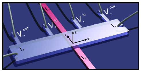
The hybrid samples consist of a 4m wide and 100 nm thick Al strip, patterned by electron-beam lithography and lift-off technique, placed perpendicularly on top of a 1.5m wide and 50 nm thick Nb wire processed by e-beam lithography and Ar ion milling (Fig. 1). In order to avoid electrical contact, the Al strip and the current-carrying Nb wire are separated by a 120 nm thick insulating Ge layer. All details of the fabrication processes are given in Ref. [37]. To investigate the spatial localization of superconductivity in the Al strip, two sets of voltage contacts were prepared at distances of 10m and 50 m from the Nb wire (the inner and outer contacts, respectively).
The normal (N) – superconductor (S) phase boundaries of the Al strip, measured in the perpendicular external magnetic field using the outer voltage contacts, are shown in Fig. 2(a) for different currents in the Nb wire, , while sending a bias current density of A/cm2 through the Al strip. To determine the superconducting transition temperature a 99% criterion of the normal state resistance was used.
When the control current is zero () and thus the magnetic field is uniform, the resulting phase boundary shows the expected linear dependence of on [black circles in Fig. 2(a)]. Due to a rather high surface to volume ratio of our mesoscopic sample and the high criterion for the determination of , it is natural to attribute the phase boundary to the appearance of surface superconductivity [38]:
| (1) |
Applying this equation to the phase transition line , measured for , we determine the superconducting critical temperature in zero field K, as well as extrapolated to the coherence length nm and the upper critical field mT, Wb is the magnetic flux quantum.
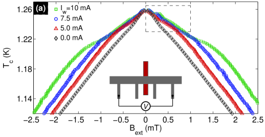
Interestingly, when the non-uniform component of the magnetic field becomes nonzero (), the phase boundaries exhibit a clear enhancement of the critical field for the whole temperature range as shown in Fig. 2(a). This enhancement becomes more pronounced as increases. Such behavior was observed for various S/F hybrids (see, e.g., review [10] and references therein). The described “magnetic bias” is commonly explained in terms of the local compensation of the applied magnetic field due to nonuniform component of the field ( if ) and trapping of the OP wave function at the locations near the minima.
To illustrate the evolution of the superconducting properties in the considered system upon varying , and , we performed numerical simulations within the two-dimensional (2D) time-dependent Ginzburg-Landau (TDGL) model [39]. For simplicity we assume that the effect of the superfluid currents on the magnetic field distribution is negligible and consider the internal magnetic field equal to the field of the external sources . This assumptions seems to be valid (i) for mesoscopic thin-film superconductors with lateral dimensions smaller than the effective magnetic penetration depth ( is the London penetration depth, is the film thickness); (ii) for superconductors at large and/or (i.e. close to the phase transition line), when the superfluid density tends to zero. In particular, the TDGL equations take the form
| (2) |
| (3) |
where is the normalized OP wave function, is the dimensionless electrical potential [40], is the vector potential [], is temperature, , is the rate of the OP relaxation, c.c. stands for complex conjugate. For the interfaces superconductor/vacuum or superconductor/insulator the boundary condition for and has the standard form
| (4) |
where is the normal vector to the sample’s boundary .
The self-consistent TDGL modelling for the superconducting sample with realistic dimensions (close to the experimental ones) is impossible because of enormous data flow. Therefore, we have restricted our consideration and analysis to a mesoscopic superconducting rectangle: length and width (e.g., if m for thin-film Al superconductors, then m and m). Since the superconducting OP wave function always has maxima near the corners of the sample [41, 42, 43], we formally have to assign at (both “left” and “right” edges). This simple technical trick guarantees that the finite length of the sample and 90∘-corners do not strongly affect those OP solutions, which are localized near the control wire and thus of main interest in the current study.
It should be noted that the field induced by the wire is antisymmetric with respect to its middle line , , therefore (i) the effective field compensation favorable for the OP nucleation occurs at positive values (i.e., on the right side of the wire) for and vice versa; (ii) . It allows us to consider only positive values without loss of generality.
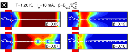


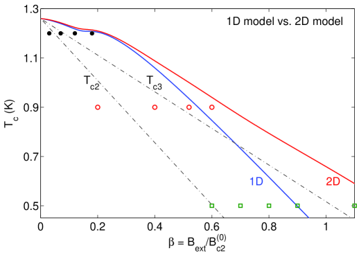
Figure 3 shows typical stationary OP distributions obtained from the TDGL model for high, intermediate and low temperatures ( K, 0.90 K and 0.50 K).
For finite and small the OP wave function expectedly nucleates far away from the control wire (see panel in Fig. 3(a), ), i.e in the area where the field induced by the wire vanishes and tends to as . At the same moment the OP nucleation near the middle line of the wire, where also , is less energetically favorable due to a larger field gradient at . The depletion of bulk superconductivity at very large distances from the wire by the applied field corresponds to a threshold value for K. The local suppression of the superconducting condensate (blue spots) at rather large distances from the wire for indicates the formation of vortices by the combined magnetic field of the control Nb wire and the applied magnetic field. For larger the OP wave function becomes more localized along the axis and trapped near the region where , remaining more or less uniform across the Al strip (panels and ). Thus, for rather high (close to ) and low , the localized OP solution moves towards the Nb wire as gradually increases, until it finally reaches the edge of the current-carrying wire. This process is accompanied by a monotonous decrease in (see Figs. 2 and 4), which is a direct consequence of a shrinkage of the typical width of the OP solution in the direction as increases (an analog of the quantum-size effect for the Cooper pairs in the nonuniform magnetic field [10]).
For lower , a completely different evolution of the superconducting properties is observed, when the inhomogeneity of the OP wave functions across the strip becomes crucial. Indeed, the formation of the localized superconducting state near the minimum of the total field, , leads to the following asymptotic behavior at : . In addition, a survival of the surface superconductivity at large distances, where , can be estimated according Eq. (1). Due to the different slopes and and the different offsets, we get the point , where both critical temperatures are equal: (the similar argumentation was presented, e.g., in [44]). Substituting (estimated for mA), we get the threshold temperature K. It means that for intermediate temperatures (K, panel (b) in Fig. 3) the gradual increase in causes subsequently the development of bulk superconducting state (the plot labelled ), the complete suppression of bulk superconductivity (), and then the suppression of surface (or edge-assisted) superconductivity at large distances from the wire and the survival of the state localized near the right edge of the wire (), since . Finally, superconductivity survives in a form of 2D patterns localized in both directions and centered at the points where the wire’s right edge intersects the superconducting sample (). In contrast to that, for low temperatures (at K, panel (c) in Fig. 3) the enhanced superconductivity along the wire’s edge is suppressed before the destruction of edge-assisted superconductivity (images and ), since in this temperature range.
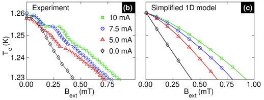
To show better the observed difference in the shape of localized OP patterns at high and low temperatures we calculate numerically the phase transition lines using the described 2D TDGL model, Eqs. (2)–(4) and 1D linearized Ginzburg–Landau (GL) equation
| (5) |
assuming and , respectively, for the same patterns and and the same boundary condition at . The used 1D model was described in detail in [19]. It is easy to see that for low and high both models give almost identical results, what supports our conclusion that the appearing OP solutions are almost uniform across the strip and the OP inhomogeneity in the direction can be disregarded. For intermediate and low temperatures and for large the phase boundaries reveal a linear behavior with different slopes: for 1D model and for 2D model. It indicates that in the limit the superconductivity is trapped both near the strip edges (in order to correspond to the slope typical for the surface superconductivity) and at the minimum of the local magnetic field (in order to explain the parallel shift of the high-field asymptote of in higher field).
Since we are mainly interested in the migration of the OP along the Al strip in low magnetic fields, we can propose a very simple description based on 1D linearized GL model, neglecting the finiteness of the Al strip in the direction [2]. If superconductivity is confined within an area where the local magnetic field can be approximated by a linear dependence , where is the point of zero total magnetic field (), for the phase boundary we obtain as a rough estimate
| (6) |
Considering the generic case of a non-uniform field , induced by an infinitely thin cylindrical wire carrying a control current , at the large distances from the wire one gets and hence
| (7) |
which seems to be valid only for low fields, , when the OP wave function is located far from the current-carrying wire. We compare the experimental data, obtained for low [Fig. 2(b)], with the results of this model [Fig. 2(c)], where we use the same parameters , and . We conclude that the 1D model works quite well for describing the suppression and the OP migration along the Al strip upon sweeping . By changing both and we directly verify that the nucleation of superconductivity is controlled not only by the local magnetic field, but also by the gradient of the field in the area where superconductivity is confined.

It is worth noting that this magnetic field profile is very similar to the field produced by a single domain wall in a thin ferromagnetic layer with out-of-plane magnetization [2]. The N-S phase boundary of a superconducting film on top of such a ferromagnetic system calculated in [2] looks very similar to that observed in our experiments. As a result, we can claim that our S/Em hybrid system behaves as a ferromagnetic film with a pinned straight domain wall with tunable saturated magnetization underneath a superconducting thin film, i.e. a situation, which cannot be easily achieved in the S/F bilayers.
Up till now we presented the superconducting properties measured with the outer voltage contacts located at the distance 50m from the Nb wire. To prove the concept of the OP localization directly, we prepared a second pair of inner voltage contacts closer to the Nb wire (10m from the wire). The results of these measurements are shown in Fig. 5. In this case to determine the phase boundary we used a 95% criterion, so that the same condition for detection of superconductivity as the 99% criterion for the 100m voltage pad separation is obtained for the inner contacts of distance 20m.
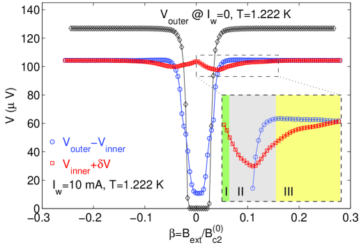
The key finding is that measured by the inner contacts is always lower than for the outer contacts, provided is rather small (up to 0.5 mT). Nevertheless the high-field asymptotes for both types of contact arrangements expectedly coincides for high fields (compare Fig. 2(a) and Fig. 5). This implies that the inhomogeneous superconductivity is located within the inner contacts for high fields and outside these contacts for low fields. Indeed, in our magnetoresistive measurements using the inner contacts at rather high temperatures and we cannot detect superconductivity nucleating outside these contacts. Therefore the measured must be lower than the critical temperature for the OP solution localized far away from the Nb wire. This is convincing experimental evidence for the field-dependent OP localization in the non-uniform magnetic field. We observed that upon increasing , the localized superconductivity shifts toward the wire, leading to a non-monotonous variation of the resistance measured between the inner contacts and, correspondingly, to the non-monotonous variation in (see Fig. 6). Unlike the reentrant dependence vs. , the voltage drop measured at the outer contacts monotonously increases as increases, since localized superconductivity always nucleates between the outer contacts and never leaves this area. Considering the inset in Fig. 6, we propose the following interpretation of our findings: in the region I the voltage drop , attributed to the area between the outer and inner contacts solely, is minimal and almost independent on , while is maximal, therefore there is no global superconductivity at this temperature in the sample and the OP wave function has to be localized between the outer and inner contacts. In the region II both and strongly depend on , and as a result, the OP wave function should be located somewhere in the vicinity of the inner contacts. Finally, in the region III the difference becomes equal to the field-independent value corresponding to the normal state and is still smaller than its normal value, therefore the OP wave function is definitely trapped between the inner contacts (i.e., near the control wire). This behavior is in good agreement with the theoretical predictions.
The position of the maximum for the inner contacts measurements can be attributed to the effective compensation of the built-in magnetic field at the inner voltage contacts. Due to the small asymmetry in the position of the voltage contacts at the opposite sides of the wire as a result of fabrication imperfections, both peaks occur at different fields: mT and mT, which is on the order of what we expect from the induced field at the voltage contacts for a current of 10 mA. More interestingly, the ’s corresponding to these peaks are slightly different, clearly showing the influence of the field gradient at the point of localization on .
Summing up, we have studied the OP localization in an Al strip subjected to an inhomogeneous field with tunable intensity induced by a current-carrying wire. The OP migration along the strip upon varying and has been detected by using multiple voltage contacts. We have shown that the critical temperature at the compensated positions is dependent on the local variation of the magnetic field. Interestingly, we demonstrate that both reentrant and non-reentrant superconducting phase boundaries can be obtained depending on where the voltage drop is recorded.
This work was supported by Methusalem Funding by the Flemish Government, and the FWO, the Carl-Zeiss-Stiftung, and the Deutsche Forschungsgemeinschaft (DFG) via the SFB/TRR 21, the Russian Fund for Basic Research, RAS under the Program ”Quantum physics of condensed matter” and FTP ”Scientific and educational personnel of innovative Russia in 2009-2013”. W.G., J.V.d.V and A.V.S. are grateful for the support from the FWO-Vlaanderen.
References
- [1] Lange M, Van Bael M J, Bruynseraede Y, and Moshchalkov V V 2003 Phys. Rev. Lett. 90, 197006.
- [2] Aladyshkin A Yu, Buzdin A I, Fraerman A A, Mel’nikov A S, Ryzhov D A, and Sokolov A V 2003 Phys. Rev. B 68, 184508.
- [3] Gillijns W, Aladyshkin A Yu, Silhanek A V, and Moshchalkov V V 2007 Phys. Rev. B 76, 060503(R).
- [4] Bulaevskii L N, Buzdin A I, Kulic M L, and Panyukov S V 1985 Adv. Phys. 34, 175.
- [5] Izyumov Y A, Khusainov M G, and Proshin Y N 2002 Phys. Usp. 45, 109.
- [6] Buzdin A I 2005 Rev. Mod. Phys. 77, 935.
- [7] Bergeret F S, Volkov A F, and Efetov K B 2005 Rev. Mod. Phys. 77, 1321.
- [8] Lyuksyutov I F and Pokrovsky V L 2005 Adv. Phys. 54, 67.
- [9] Velez M, Martin J I, Villegas J E, Hoffmann A, Gonzalez E M, Vicent J L, and Schuller I K 2008 J. Magn. Magn. Mater. 320, 2547.
- [10] Aladyshkin A Yu, Silhanek A V, Gillijns W, and Moshchalkov V V 2009 Supercond. Sci. Technol. 22, 053001.
- [11] Buzdin A I and Mel’nikov A S 2003 Phys. Rev. B 67, 020503.
- [12] Yang Z, Lange M, Volodin A, Szymczak R, and MoshchalkovV.V., Nature Materials 3, 793 (2004).
- [13] Werner R, Aladyshkin A Yu, Guénon S, Fritzsche J, Nefedov I M, Moshchalkov V V, Kleiner R, and Koelle D 2011 Phys. Rev. B 84, 020505(R).
- [14] Yang Z, Vervaeke K, Moshchalkov V V and Szymczak R 2006 Phys. Rev. B 73, 224509
- [15] Yang Z, Van de Vondel J, Gillijns W, Vinckx W, Moshchalkov V V and Szymczak R 2006 Appl. Phys. Lett. 88, 232505.
- [16] Fritzsche J, Moshchalkov V V, Eitel H, Koelle D, Kleiner R, and Szymczak R. 2006 Phys. Rev. Lett. 96, 247003.
- [17] Aladyshkin A Yu, Fritzsche J, and Moshchalkov V V 2009 Appl. Phys. Lett. 94, 222503.
- [18] Aladyshkin A Yu, Fritzsche J, Kramer R B G, Werner R, Guénon S, Kleiner R, Koelle D, and Moshchalkov V V 2011 Phys. Rev. B 84, 094523.
- [19] Aladyshkin A Yu and Moshchalkov V V 2006 Phys. Rev. B, 74, 064503.
- [20] Aladyshkin A Yu, Volodin A P and Moshchalkov V V 2010 J. Appl. Phys. 108, 033911.
- [21] Yang Z, Fritzsche J, and Moshchalkov V V 2011 Appl. Phys. Lett. 98, 012505.
- [22] Milosevic M V, Gillijns W, Silhanek A V, Libal A, Peeters F M and Moshchalkov V V 2010 Appl. Phys. Lett. 96, 032503 (2010).
- [23] Vlasko-Vlasov V, Welp U, Karapetrov G, Novosad V, Rosenmann D, Iavarone M, Belkin A, and Kwok W-K 2008 Phys. Rev. B 77, 134518.
- [24] Vlasko-Vlasov V K, Welp U, Imre A, Rosenmann D, Pearson J, and Kwok W K 2008 Phys. Rev. B 78, 214511.
- [25] Zhu L Y, Chen T Y, and Chien C L 2008 Phys. Rev. Lett. 101, 017004.
- [26] Ozmetin A E, Yapici M K, Zou J, Lyuksyutov I F, and Naugle D G 2009 Appl. Phys. Lett. 95, 022506.
- [27] Belkin A, Novosad V, Iavarone M, Fedor J, Pearson J E, Petrean-Troncalli A and Karapetrov G 2008 Appl. Phys. Lett. 93, 072510.
- [28] Belkin A, Novosad V, Iavarone M, Divan R, Hiller J, Proslier T, Pearson J E, and Karapetrov G 2010 Appl. Phys. Lett. 96, 092513.
- [29] Gillijns W, Aladyshkin A Yu, Lange M, Van Bael M J, and Moshchalkov V V 2005 Phys. Rev. Lett. 95, 227003.
- [30] Gillijns W, Silhanek A V, and Moshchalkov V V 2006 Phys. Rev. B 74, 220509.
- [31] Silhanek A V, Gillijns W, Milosevic M V, Volodin A, Moshchalkov V V, and Peeters F M 2007 Phys. Rev. B 76, 100502.
- [32] de Gennes P G , 1966 Superconductivity of Metals and Alloys (W. A. Benjamin Inc., New York).
- [33] Bremer J W 1962 Superconductive Devices (McGraw-Hill, New York).
- [34] J. M. Lock, Rep. Prog. Phys. 25, 37 (1962).
- [35] Newhouse V L 1969 in Superconductivity, edited by R.D. Parks (Marcel Dekker, New York, 1969), Vol. 2, Chap. 22.
- [36] Pannetier B, Rodts S, Genicon J L, Otani Y, and Nozieres J P 1995 in Macroscopic Quantum Phenomena and Coherence in Superconducting Networks, edited by C. Giovannella and M. Tinkham (World Scientific, Singapore), pp. 17.
- [37] Aladyshkin A Yu, Ataklti G W, Gillijns W, Nefedov I M, Shereshevsky I A, Silhanek A V, Van de Vondel J, Kemmler M, Kleiner R, Koelle D, and Moshchalkov V V 2011 Phys. Rev. B 83, 144509.
- [38] Saint-James D, Sarma G., and Thomas E.J. 1969 Type-II superconductivity (Pergamon Press).
- [39] The described simulations were performed using the Windows-oriented solver GLDD, developed in the Institute for Physics of Microstructures RAS.
- [40] We use the following units: for time, the coherence length at temperature for distances, for the vector potential; for the electrical potential, and for the current density, where and are the conventional parameters of the GL expansion, and are charge and the effective mass of carriers, is the normal state conductivity.
- [41] Houghton A, McLean F B 1965 Phys. Lett. 19, 172; van Gelder A. P. Phys. Rev. Lett. 1968 20, 1435.
- [42] Schweigert V. A. and Peeters F. M. 1999 Phys. Rev. B 60, 3084.
- [43] Chibotaru L F, Ceulemans A, Morelle M, Teniers G, Carballeira C and Moshchalkov V V 2005 Journ. Math. Phys. 46, 095108.
- [44] Aladyshkin A Yu, Ryzhov D A, Samokhvalov A V, Savinov D A, Mel’nikov A S and Moshchalkov V V 2007 Phys. Rev. 75, 184519.