A New Formal Approach for Predicting Period Doubling Bifurcations in Switching Converters
Abstract
Period doubling bifurcation leading to subharmonic oscillations are undesired phenomena in switching converters. In past studies, their prediction has been mainly tackled by explicitly deriving a discrete time model and then linearizing it in the vicinity of the operating point. However, the results obtained from such an approach cannot be applied for design purpose. Alternatively, in this paper, the subharmonic oscillations in voltage mode controlled DC-DC buck converters are predicted by using a formal symbolic approach. This approach is based on expressing the subharmonic oscillation conditions in the frequency domain and then converting the results to generalized hypergeometric functions. The obtained expressions depend explicitly on the system parameters and the operating duty cycle making the results directly applicable for design purpose. Under certain practical conditions concerning these parameters, the hypergeometric functions can be approximated by polylogarithm and standard functions. The new approach is demonstrated using an example of voltage-mode-controlled buck converters. It is found that the stability of the converter is strongly dependent upon a polynomial function of the duty cycle.
Index Terms:
DC-DC Converters, Hypergeometric Series, Hypergeometric Functions, Polylogarithm Functions, Voltage Mode Control, Period Doubling, Subharmonic Oscillations.I Nomenclature
Let us define the following parameters related to the buck switching regulator studied in this work and that are listed in analphabetic order.
| Ratio between and | |
| Output Capacitance | |
| Steady state duty cycle | |
| Switching frequency | |
| Zero due to the ESR | |
| Proportional gain | |
| Inductance | |
| Damping quality factor | |
| Load resistance | |
| ESR of the capacitance | |
| ESR of the inductance | |
| Switching period | |
| Input source voltage | |
| Angular resonance frequency | |
| Pole of the type II controller | |
| Angular switching frequency | |
| Zero due to the ESR of output the capacitor | |
| Zero of the PI controller |
II Introduction
Switching converters are integral elements to modern power electronics. Despite their widespread use, they can pose serious challenges to power-supply designers because almost all of the rules of thumb governing their design are only applicable to the linearized averaged system even though the system works in switched mode [1], [2]. Switch mode operation is carried out by means of Pulse width Modulation (PWM) action on the switches. In the traditional PWM control, the duty cycle of the pulse driving signal is varied according to the error between the output voltage and its desired reference. This error is processed through a compensator to provide the control voltage . The simplest analog form of generating a fixed frequency PWM is by comparing the control voltage with a ramp periodic signal in such a way that the pulse signal goes high/low when the control signal is higher/lower than the triangular signal. A rising ramp carrier will generate a PWM signal with trailing edge modulation and a falling ramp carrier will generate a PWM signal with leading edge modulation [3]. In the trailing edge modulation strategy, when the control voltage is greater (resp. smaller) than the sawtooth ramp voltage, the switch is ON (resp. OFF). Whereas in the leading edge modulation strategy, the opposite happens. Figure 1 shows a schematic circuit diagram of a buck converter under voltage mode control with a compensator and a fixed frequency PWM and its equivalent block diagram.
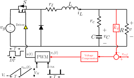
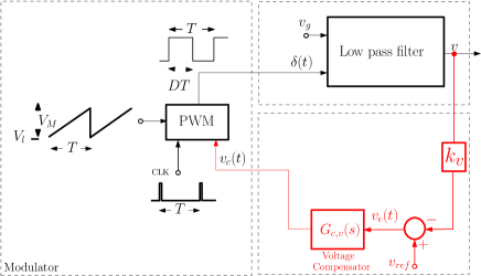
Probably, the buck converter is the most common voltage regulator in use. Its structure is not complicated (See Fig. 1-(b)). The power stage together with the modulator consists of a pulse generator and a passive low pass filter. For this reason, it can be used to convert an input source voltage into a lower output voltage . In order to regulate the output voltage, a voltage reference, an error detector, a compensator and a modulator are added to the circuit. These basic elements form a complete switching buck DC-DC regulator.
In practice, it is desirable that the system operates periodically with a constant switching frequency equal to that of the external sawtooth ramp modulating signal which is the same frequency of the external clock signal. However, under parameter changes, the stability of this operating mode may be lost resulting in different kinds of instabilities and dynamical behaviors [4]-[12]. There have been hitherto many research efforts devoted to predict the border of occurrence of such instabilities. However, in the case of subharmonic oscillations in voltage mode control, most of the reported analysis are based on abstract mathematical models, which are demonstrated to be very powerful to accurately predict this phenomenon, but not so suited to obtain clear design-oriented criteria in the parametric design space. In the past studies, the prediction of subharmonics is mainly based on deriving an accurate discrete time model and then linearizing it in the vicinity of the operating point. However, the results obtained from such an approach cannot be applied for design purpose. Recently, Filippov’s method and the monodromy matrix were used to predict these instabilities in DC-DC converters and similar results to those obtained from the discrete time approach were derived [13], [14].
While there are powerful design-oriented techniques to characterize low frequency instabilities related to the averaged model [1], there is still a lack of design oriented tools for predicting fast scale instability in the form of period doubling and subharmonic oscillations inherent to the switched nature of the system. Note that this phenomenon can be perfectly predicted in the peak and the valley current-mode-controlled system examining mainly the slopes of the inductor current ([1]) or by using modified averaged models taking into account delay terms due to the sample-and-hold effect ([15]) but not in voltage mode control or in average current mode control [16], [17]. For example, it is known that to guarantee the stability of a peak current-mode-controlled buck converter, the following inequality, in terms of the duty cycle and the system parameters, must hold
| (1) |
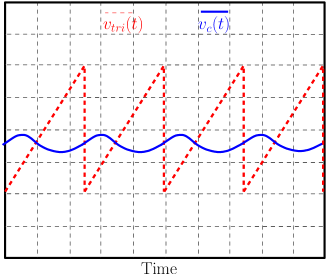
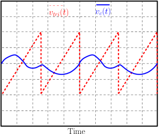
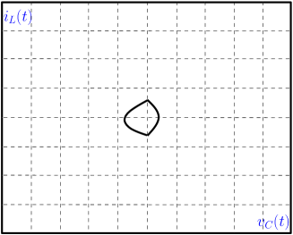
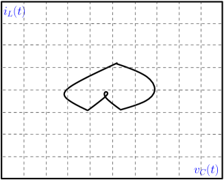
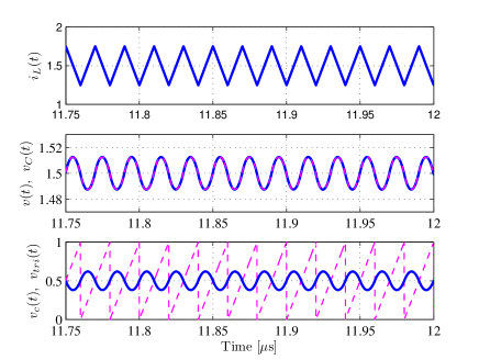
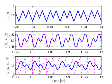
On the other hand, voltage mode controlled power supply has become very popular especially in low noise next generation communication systems. Such systems are supplied by means of different Point of Load (PoL) voltage regulators in the form of single phase voltage-mode-controlled buck converters [18]-[19]. It is well known that these converters, under voltage mode control, are prone to exhibit undesired subharmonic oscillations for certain parameter values [4], [6], [8]. Figure 2 shows typical waveforms and state plane trajectories for the desired periodic behavior and for subharmonic oscillations in a voltage-mode-controlled buck converter.
An equivalent expression to (1), in the case of voltage mode control, will be extremely helpful in designing switching converters free from subhamonic oscillations. One may, therefore, ask: There exists a similar expression as (1) for the case of the voltage-mode-controlled system? This paper tries to develop such an expression for different voltage mode control schemes.
The rest of this paper is organized as follows: a short tutorial on hypergeometric series and their special case, polylogarithm functions, is given in Sections III. Section IV will revisit the dynamic model of the buck converter in the frequency domain and conditions for periodic behavior and subharmonic oscillations are presented in this domain by using Fourier series. These series are calculated exactly by using hypergeometric functions and approximately by using polylogarithmic functions. The approach is then applied, in Sections V, to a voltage-mode-controlled DC-DC buck converter with different controller transfer functions. Some circuit-based simulations are presented to validate the results obtained from the derived theoretical results. In Section VI, the results are formulated in terms of Figures of Merit, widely used by the power electronic community, such as the crossover frequency and the phase margin. Finally, in the last section, some concluding remarks of this work are summarized.
III A Short Tutorial on the hypergeometric and polylogarithm functions
III-A Gamma function
It is somewhat problematic that a large number of definitions have been given for the gamma () function [20]. Although they describe the same function, it is not entirely straightforward to prove their equivalence. One of the definitions of the gamma function due to Euler is [20]
| (2) |
Using integration by parts, one can show the recursive relation in such a way that for integer numbers , . The Euler gamma function is one of the most important functions in mathematical physics [20]. It may be regarded as a generalization of the factorial which spreads its values over the whole complex plane, except at the negative integers.
III-B Psi digamma function
III-C Pochhammer’s Symbol
The Pochhammer symbol is defined as the ratio between and [20], i.e
| (4) |
III-D Generalized hypergeometric functions
A generalized () order hypergeometric function is defined as a power series of the complex number . The expression of such function can be written in the form [20]
| (5) |
Many calculus packages such as Mathematica [21], Maple [22] and Matlab [23] have routines to compute these hypergeometric functions. Yet, theses functions have interesting properties and in some cases they can be converted to polylogarithms which when evaluated at the unit circle can be expressed by standard functions [24].
III-E Polylogarithm functions
For some specific values of and in (5), the hypergeometric functions can be converted to polylogarithm functions [25]. The polylogarithm, also known as the Jonquiére’s function (See [26]), is the function defined in the complex plane over the open unit disk by
| (6) |
For , one simply obtain . The polylogarithm function is connected to the generalized hypergeometric functions through the relation [24]
More specifically, one has [24]
| (7) | |||||
| (8) |
III-F Polylogarithm on the unit circle
For , (), the polylogarithm functions can be expressed as , where , and . One has the following first and functions [20]
| (9) | |||||
| (10) | |||||
| (11) |
It will be shown later that (9)-(11) are the polynomial functions that appear in the expressions establishing the boundary condition for subharmonic oscillations occurrence in the buck converter. While the first one (9) corresponds to the peak and valley current mode control, the second and the third ones (10)-(11) appear in both voltage mode control and current mode control with dynamic compensator such as average current mode control [16].
III-G The Riemann Zeta function
It is the function defined by [20]
For example, for , . It can be proved that one has the following values of for even integer arguments [20]
where are called Bernoulli numbers [27]. Explicit formulas for the values for odd integer arguments are not available and currently it seems that this is a very difficult problem for mathematicians. In fact, it is only proved that is an irrational number known as the Apéry’s constant. For engineering use, the fact that converges quickly to 1 can be used to approximate by 1 for .
IV Buck converter under voltage mode controller
The reader may now ask why all previous rather theoretical material is presented? Simply because these functions will appear in the mathematical expressions describing the periodic behavior and the subharmonic oscillations in the buck converter. The presentation of this theoretical material will allow to the reader a better understanding of the results presented in this paper.
IV-A Dynamic model of the power stage circuit
Consider a buck converter under voltage mode control shown in Fig. 1-(a) that can be equivalently represented by the block diagram shown in Fig. 1-(b). For simplicity, let us suppose that and and that the load is purely resistive (). The approach can be extended to other more complex models of the loads and reactive components but at the expense of more mathematical involvement. For the considered case, the buck regulator power stage input-to-output (-to-) transfer function can be expressed in the following generalized form [1]
| (12) |
All the parameters that appear in the expression of the transfer function (12) are given in a list of parameters given at the beginning of the this work. is given by
Theoretically, parasitic parameters can be easily ignored. However, the first order parasitic elements such as ESRs of the inductor and the output capacitor are included in the analysis. The effect of these parasitic elements may be insignificant in some cases but it may be dramatic in others. Engineering judgement can be done once included to examine their effects.
IV-B Closed form conditions for periodic behavior and subharmonics
Let be the compensator transfer function from the error to the control voltage . Let be the steady state duty cycle and , where for trailing edge modulation and for leading edge modulation. Let be the lower value of the triangular ramp modulator signal , its amplitude and its period. Let and . Let us also define .
It can be recognized that the voltage at the input of the low pass filter is essentially a square wave with amplitude . The period of this signal depends on the dynamics of the closed loop system. Expanding this square wave in a Fourier series and operating on each term , equating the resulting expression to the ramp signal at the switching instants defined by the crossing between and , conditions for different periodicity can be obtained. This approach has been applied in [28] to obtain the following condition for periodic behavior.
| (13) |
where and stands for taking the real part. In [28], it has been also shown that at the boundary of subharmonic oscillations, the following equality holds
| (14) |
The system of equations (13)-(14) can be solved for any design parameter to locate the boundary between the desired stable periodic behavior and subharmonic oscillations. This equation can be solved either graphically by plotting (13) and (14) for a sufficiently high number of terms and looking at the intersection point, by numerical methods or analytically for some limit cases as it will be shown later.
In [28], the series in (13)-(14) have been approximated by the term that involve the transfer function with the smallest argument or solved graphically by truncating the series. In this work, closed form expressions will be given for the series involved in (13) and (14). To calculate the series, it is required to use the concept of hypergeometric series and polylogarithm functions presented in Section II. It will be shown later that by considering practical operating conditions, these series can be approximated by standard functions depending on the power stage and controller parameters and more importantly on the steady state value of the duty cycle .
IV-B1 Conditions for periodic behavior
From (13), an expression for the input voltage in terms of the circuit parameters and the duty cycle for the periodic regime is
| (15) |
From (15) and (13), is a small quantity depending on given by
| (16) |
where stands for taking the imaginary part. Without , (15) represents the well-known relationship between the input and the output voltages of the averaged model of a buck converter. Therefore, the term represents a correctional factor that determines the difference between the averaged model and the reality of the switched system in the case of periodic regime. Note that the same approach is valid for determining other critical parameter values, such as the feedback gain, ramp amplitude and reference voltage.
IV-B2 Conditions for subharmonic oscillations
Similarly, from the equation establishing the subharmonic oscillations boundary (14), the input voltage at this boundary is
| (17) |
where from (14), is given by
| (18) |
The function depends on the controller used. In the next sections, closed form expressions will be given for and for different controller transfer functions. These expressions will be derived exactly in terms of hypergeometric functions and approximately by using polylogarithms and their special expressions on the unit circle using Eqs. (9)-(11).
V Application to a buck converter under voltage mode control
V-A Buck converter under a simple proportional controller
It is instructive to start the application of the approach to a buck converter with a simple proportional controller. In this case, the controller transfer function is simply a constant for all the frequencies (). Both trailing edge modulation and leading edge modulation are studied in a unified approach. The results obtained for the leading edge modulation case can be applied directly to the trailing edge modulation case by simply changing by .
Let us consider that the output capacitor is ideal. However, the results for this simple case will be valid for a buck converter with a realistic output capacitor and under a single pole controller with a pole located at exactly the zero due to the ESR of the output capacitor.
V-A1 Condition for periodic oscillations
By using (12) and (16), the expression of can be written in the following hypergeometric-function-based form
| (19) | |||||
where and . For this controller, , and (15) becomes
| (20) |
Due to the pole-zero cancelation, this is the same expression that would be obtained for a single pole controlled buck converter with an ESR in the output capacitor.
In a practical design, and and then, and . Then, (19) becomes
| (21) |
where is the Apéry’s constant ([29]). After calculating the specific hypergeometric series, (21) gives
| (22) |
is the trilogarithm function defined in general by (6). The imaginary part of the trilogarithm evaluated at the unit circle is the function defined in (11) and therefore one has from (22)
| (23) |
For design purpose, can even be ignored because the first term in the denominator of (20) is dominant. In fact it can be proved that for the whole operating range of the duty cycle and therefore the input voltage will be related to the duty cycle , in the case of a single pole controller canceling the ESR zero or in the case of a simple proportional controller, by the following approximated expression
| (24) |
Note that this is the same expression that one would obtain if a simple averaged model is used. For design-oriented analysis (24) is accurate enough while an approximated expression for is still available in terms of standard functions. Indeed, if is substituted by its expression in (11) and by using (20), another approximated closed form expression for is
| (25) |
Note that both (24) and (25) are approximated expressions while the exact equation is (20).
V-A2 Condition for subharmonic oscillations
Following a similar procedure to that of the previous section, an expression for in (18) can be obtained. For the case of single pole controller canceling the zero due to the ESR of the output capacitor or in the case of a simple proportional controller and an ideal output capacitor, from (12) and (17) is given by the following hypergeometric-function-based expression
| (26) | |||||
Under the practical conditions, and , (26) becomes
| (27) |
By calculating the special hypergeometric series that appears in (27), can be written in the following dilogarithm-based expression
| (28) |
Using (17) and (28), the critical input voltage giving the boundary of subharmonic oscillation in terms of the duty cycle is obtained
| (29) |
Taking the real part of the dilogarithm function using (10) and substituting , the following expression is obtained for both the leading edge modulation and the trailing edge modulation modulation strategies
| (30) |
which is the same expression obtained in [33] for the case of ideal components ( and ) by using a very different approach. Note that and in (30) depends on the parasitic parameters. The critical value of the input voltage depends on both power stage and control system parameters and most importantly on the duty cycle .
From (30), subharmonic oscillations can be avoided in the system if the following inequality holds
| (31) |
where is a second degree polynomial function of the duty cycle and is a function of the vector of the system parameters. Eq. (31) can be considered as an extended expression to (1) for the voltage-mode-controlled buck converter. It can be observed that (31) is invariant under the change which implies that the same expression is valid for both leading edge modulation and trailing edge modulation strategies. To validate the previous theoretical predictions, let us consider the following example.
Example 1
Consider the well known and widely studied example of buck converter considered first in [4] and later by other researchers in [7], [8], [9], [13]. The same set of parameter values will be considered so that the readers can make the comparison easily. Namely, mH, F, V, V, s, V and . Furthermore, numerical simulations are not repeated here to save space. Interested readers can see [13] and [14] for both numerical simulations and experimental measurements.
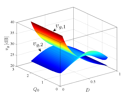
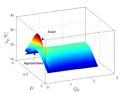
Figure 3-(a) shows a mesh plot of from (17) and from (15) in terms of the duty cycle and the quality factor or equivalently the load resistance . The intersection of the two surfaces is the curve of the critical input voltage at the boundary of subharmonic oscillations. In Fig. 3-(b), the exact mesh plot of from (17) is shown together with the approximated plot from (30). From this figure, it can be observed that for small , a discrepancy exists between the exact and the approximated plots. This discrepancy becomes significant for a power quality approaching . For , (30) will give inaccurate results. In fact, the main drawback of the simplified expression based on (30) is that it practically does not depend on the load resistance which is an important design parameter111Note that the unique dependence of the simplified expression of on is through the parameter ..
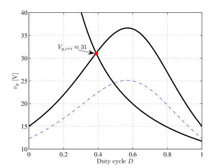
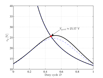
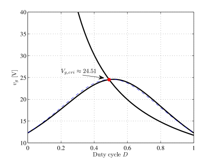
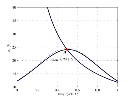
Figure 4 shows the exact plots of and from (15) and (17) and the approximated plots from (25) and (30) for different values of the load resistance . For all the considered values of this parameter, the curves of using (15) and (25) are practically coincident. However, concerning , it can be observed that there is a discrepancy between the exact curve and the approximated one for low values of the load resistance.
The critical value of the input voltage is the intersection of the curves from (15) and from (17). It can be determined by simply subtracting from , equating the resulting expression to zero and solving for and then substituting in or in . For instance, for (Fig. 4-(c)), the critical value of the input voltage V (for ) which is in perfect agreement with [8], [13], [14]. For this value of the load resistance, and the critical value can be also obtained accurately from the approximated expression.
As decreases, the value of intersection point increases as predicted in [13] by using a different approach based on Fillipov method and the monodromy matrix. For example, for 5 , the critical value of the input voltage is approximately 31 V which is in perfect agreement with [13] (See Fig. 7 in [13]). From the approximated expression of one still obtains V. This discrepancy is due to the low value of .
Note that the symmetry with respect to is lost for low values of the quality factor which does not appear in (30). Also, the maximum value of moves to the right side of , when decreases in the case of leading edge modulation while it moves to the left side in the case of trailing edge modulation.
V-B Buck converter under a PI controller
A simple dynamic compensator that remove the steady state error from the system under a proportional control, can be obtained by adding a pole at the origin. Also a zero is added to improve the phase margin. The resulting controller is a Proportional-Integral (PI) compensator and generally has the following transfer function
| (32) |
The added zero is selected to be at () [31], [32]. Note that the total loop transfer function will be the same one corresponding to a Type II controller with an aditional pole canceling the zero due to the ESR of the output capacitor [32]. The exact expression of can also be expressed by (15), where is also given by a generalized hypergeometric function and can be approximated by polylogarithms. However, as and are infinite for this type of controllers due to the pole at the origin, from (15), can be approximated by which is a very simple and well known expression for relating the input and the output voltages in a buck converter that can also be obtained from a conventional averaged model [1]. Following a similar procedure as for the case of a simple proportional controller, the exact expression of in this case is also given by a hypergeometric function. The same expression of (17) is valid in this case with depending on a new parameter and given by the following expression
| (33) | |||||
Note that when , , and . To obtain a more simple expression for in the case of a type II and PI controllers, let us consider and , which is the case in almost all practical designs. Therefore, in terms of polylogarithms, (33) becomes as follows
| (34) |
It can be noted that, as (), the contribution due to the trilogarithm term is actually negligible. The real part of the dilogarithm and the imaginary part of the trilogarithm have been already obtained before. Therefore, for the case of Type II and the PI controllers with a trailing edge modulation (), the approximated critical value of the feedback gain has the following expression
| (35) |
Similar analysis can be applied to obtain the expression corresponding to a leading edge modulation strategy. Note that the symmetry with respect to is lost although this cannot be appreciated since is very small in practice. Equation (35) can be considered as an extension of (30) for the case of the Type II and the PI controllers. The next example validates the results for a buck converter for these two different controllers.
Example 2
Consider a buck converter with voltage mode control and trailing edge modulation studied in [33] whose value of parameters are oriented to miniaturization. The considered fixed parameters in this example are: , nH, nF, MHz, 0, 1 V, V and . Two cases will be studied. In the first one, ideal output capacitor and inductor are considered and the system will be under a PI control. In the second case, parasitic elements will be included. While for the ESR of the inductor, only static performances are changed, in the case of an ESR of the output capacitor, a zero is introduced in the dynamic model of the system. This zero is canceled with an additional of the type II controller. Note that although the dynamic effect of the ESR output capacitor zero is canceled, its static effect still appears in the expression of since depends on this parameter.
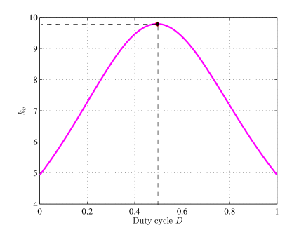
V-B1 Ideal components
The system in this case is under a PI controller. Furthermore, in order to do not induce slow scale instability, let us select such that the zero () of the PI controller be below [33]. Therefore, it will be below because in a practical design. Figure 5-a shows the stability curve (35) in terms of the proportional gain and the duty cycle . From (35), the critical value of the feedback gain for the previous set of parameter values with V (), is .
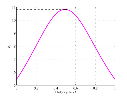
V-B2 Taking into account parasitic elements
Let us consider that 0.05 and 1 m. The system in this case is under a Type II controller. Its additional pole is selected at exactly . As before the zero of the PI controller is below . Figure 5-(b) shows the stability curve in terms of the proportional gain and the duty cycle from (35). The critical value of the feedback gain for the previous set of parameter values with V () is .
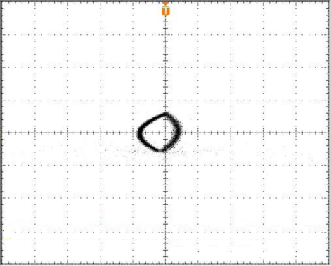
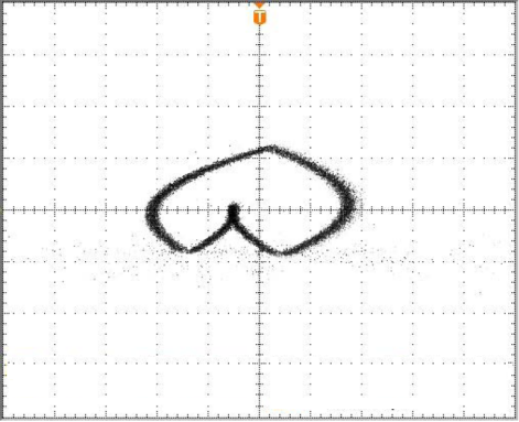
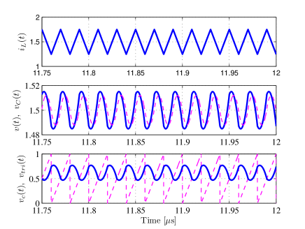
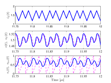
Figure 6-(a)-(d) shows the time domain numerical simulation for the two previous cases for value of the feedback gain just before and just after subharmonic oscillations occurrence. These numerical simulations are in perfect agreement with the theoretical derivations.
VI Design-oriented prediction of subharmonic oscillations
VI-A Crossover frequency as a Figure of Merit
The closed form results presented previously can be interpreted in terms of several Figures of Merit like for example the ripple amplitude in [33]. The results can be also interpreted by the crossover frequency and the associated phase margin which depends on the controller used. The crossover frequency is defined as the frequency where the modulus of the loop gain crosses 0 dB (). For instance, for the buck converter under the proportional, PI and Type II controllers, the crossover frequency can be approximated by
| (36) |
Note that increasing the proportional gain or decreasing the modulator amplitude will raise the crossover frequency but this can also cause subharmonic oscillations. From (30) and (36), the boundary conditions for this phenomenon, in terms of the crossover frequency can be written in the following general form
| (37) |
where depends on the controller used. For the case of proportional, PI and Type II controllers and if and , from (30), can be approximated by
| (38) |
From (36), the condition for the system to be free form subharmonic oscillations will be
| (39) |
In [30], the upper limit of the crossover frequency is discussed. For an ideal converter it was recommended, without demonstration, that an upper limit is . Eq. (39) establish a theoretical upper limit for avoiding subharmonic oscillations in the buck converter.
VI-B Phase margin as a Figure of Merit
Traditionally, the phase margin is used, as a test on the loop gain , to determine the stability of the closed loop system in the averaging context. The phase margin is determined from the phase of at the crossover frequency , by
| (40) |
If crosses 0 dB only once, then the closed loop system , the system will not present slow scale instability that can be predicted by a simple averaged model. Traditionally a phase margin of at least is required to guarantee an acceptable system response [1], [31], [32]. Furthermore, to avoid subharmonic oscillations, the phase margin must be greater than in (39).
Note that the phase margin will depend on the type of the controller used and the system parameters. From (39) and (40), the general expression of the critical phase margin can be written in the following form
| (41) |
Subharmonic oscillations can be avoided if . For , a well designed converter based on the loop gain analysis of the averaged model will not exhibit subharmonic oscillations. For , subharmonic oscillation may still occur even for a well designed converter.
Conclusions
Subharmonic oscillations in peak-current-mode-controlled converters are well documented by different analytical methods. However, in voltage mode control, this phenomenon has been only characterized by using numerical simulations or mainly based on abstract mathematical analysis using a discrete time model or the Fillipov method. Both approach do not allow to relate the results to concepts that are familiar to power electronics engineers. Explicit expressions for conditions of subharmonic oscillations occurrence have been unavailable for many years.
It is widely known that for peak current mode control without ramp compensation, for example, the stability condition is . This expression is shown to be a special case of the general results presented in this paper. In general, it can be conjectured that the stability condition is in the form , where is a function of the duty cycle that can be approximated by a polynomial function and is a function of the vector of system parameters . It was also shown that the structure of the loop gain offers some additional insights on issues related to the stability of the system. Interestingly, the degree of the polynomial function is extremely related to the relative degree of the total loop transfer function. For instance, for peak current mode control, the relative degree of the total loop gain is 1 and the degree of is also 1. For voltage mode control, the relative degree of the loop gain depends on the compensator. For proportional controller, single pole controller canceling the ESR zero of the power stage and for PI controller, the relative degree of the total loop is 2 and can also be approximated by second degree polynomial function. The same can be conjectured for total loop transfer functions corresponding to other control schemes such as average current mode.
Based on the approach presented in this study, critical values of the system parameters can be located accurately. Only in special limiting cases, an analytical solution can be obtained. Analytical methods end at a certain point and have to be succeeded by numerics in the general case. However, hypergeometric-based functions have some physical insights on how the system parameters affect the dynamics and how approximations should be done to predict subharmonic oscillations in an analytical way in the case of a quality factor . Furthermore, by guaranteeing the stability for a high case, the stability is also guaranteed for the low case.
After explicitly obtaining the conditions for subharmonic oscillation, the results have been reformulated in terms of Figures of Merit widely used by the power electronics community, such as the crossover frequency, and phase margin. The critical expressions for these Figures of Merit can be obtained in terms of converter parameters and its controller. The ability to predict subharmonic instability using pure algebraic equations directly expressible in terms of such Figures of Merit is a major advantage of the proposed approach.
Works are in progress to extend the approach to other switching converter topologies and other control schemes. The results will be reported in a further study.
References
- [1] R. Erickson and D. Maksimovic, Fundamentals of Power Electronics, 2nd ed. Springer, 2001.
- [2] B. Lehman , and R. M. Bass, “Switching Frequency Dependent Averaged Models for PWM DC-DC Converters,” IEEE Trans. on Power Electronics, vol. 11, no. 1, pp. 89-98, 1996.
- [3] Z. Lai, and K. M. Smedley, “A General Constant-Frequency Pulsewidth Modulator and Its Applications,” IEEE Transactions on Circuits and Systems I: Regular Papers, vol. 45, no. 4, pp. 386-396, 1998.
- [4] D. C. Hamill, J. H. B. Deane and D. J. Jefferies, “Modelling of Chaotic DC-DC Converters by Iterated Nonlinear Mapping, IEEE Transactions on Power Electronics, vol. 7 no. 1, pp. 25-36, 1992.
- [5] E. Toribio, A. El Aroudi, G. Olivar, and L. Benadero, “Numerical and Experimental Study of the Region of Period-one Operation of a PWM Boost Converter,” IEEE Trans. on Power Electronics, vol. 15, no. 6, pp. 1163-1171, 2000.
- [6] A. El Aroudi A., M. Debbat, G. Olivar, L. Benadero, E. Toribio, & R. Giral, “Bifurcations in DC-DC Switching Converters, Review of Methods and Applications,” Int. J. Bifurcations & Chaos vol. 15, no. 5, 1549–1578, 2005.
- [7] C. K. Tse, Complex Behavior of Switching Power Converters, Boca Raton, USA: CRC Press, 2003.
- [8] M. di Bernardo, F. Garefalo, L. Glielmo, and F. Vasca, “Switchings, Bifurcations, and Chaos in DC/DC Converters,” IEEE Transactions on Circuits and Systems I: Fundamental Theory and Applications, vol. 45, no. 2, pp. 133–141, 1998.
- [9] E. Fossas and G. Olivar “Study of Chaos in the Buck Converter,” IEEE Transactions on Circuits and Systems I: Fundamental Theory and Applications, vol. 43, no. 1, pp. 13–25, 1996.
- [10] A. El Aroudi, B. Robert, A. Cid-Pastor and L. Martínez-Salamero, “Modelling and Design Rules of a Two-Cell Buck Converter Under a Digital PWM Controller,” IEEE Transactions on Power Electronics, no. 23, vol. 2, pp. 859–870, 2008.
- [11] A. Kavitha and G. Uma, “Experimental Verification of Hopf Bifurcation in DC-DC Luo Converter,” IEEE Transactions on Power Electronics, no. 23, vol. 6, pp. 1–6, 2008.
- [12] B. Bao, G. Zhou, J. Xu, and Z. Liu, “Unified Classification of Operation State Regions for Switching Converters with Ramp Compensation,” IEEE Transactions on Power Electronics, to be published.
- [13] D. Giaouris, S. Banerjee, B. Zahawi, V. Pickert, “Stability Analysis of the Continuous-Conduction-Mode Buck Converter Via Filippov’s Method”, IEEE Transactions on Circuits and Systems I: Regular Papers, vol. 55, no. 4, pp. 1084-1096, 2008.
- [14] D. Giaouris, S. Maity, S. Banerjee, V. Pickert, and B. Zahawi, “Application of Filippov Method for the Analysis of Subharmonic Instability in DC-DC converters,” International Journal of Circuit Theory and Applications, vol. 37, no. 8, pp. 899-919, 2009.
- [15] R. Ridley, “A New, Continuous-Time Model for Current-Mode Control,” IEEE Trans. Power Electronics, vol. 6, no. 2, pp. 271–280, 1991.
- [16] W. Tang, F. Lee, and R. Ridley, “Small-signal modeling of average current-mode control,” IEEE Trans. Power Electronics, vol. 8, no. 2, pp. 112–119, 1993.
- [17] L. Dixon, “Average Current Mode Control of Switching Power Supplies,” Unitrode Corp., Merrimack, NH, Unitrode Application Note, U-140.
- [18] Y. Panov and M. M. Jovanovic, “Design Considerations for 12-V/1.5-V, 50-A Voltage Regulator Modules,” IEEE Transactions on Power Electronics, no. 6, vol. 16, pp. 776-783, 2001.
- [19] J. Sun, “Characterization and Performance Comparison of Ripple-Based Control for Voltage Regulator Modules,” IEEE Transactions on Power Electronics, no. 2, vol. 21, pp. 346-353, 2006.
- [20] M. Abramowitz and I. A. Stegun, eds. Handbook of Mathematical Functions with Formulas, Graphs, and Mathematical Tables. New York: Dover, 1972.
- [21] www.wolfram.com/mathematica/
- [22] www.maplesoft.com/
- [23] www.mathworks.com/
- [24] L. C. Maximon, “The Dilogarithm Function for Complex Argument,” Proceedings: Mathematical, Physical and Engineering Sciences, vol. 459, no. 2039. pp. 2807-2819. 2003.
- [25] Lewin, L. Polylogarithms and Associated Functions. New York: North-Holland, 1981.
- [26] A. Jonquiére, “Note sur la Série ,” (in French). Bulletin de la Société Mathématique de France, vol. 17, pp. 142-152, 1889.
- [27] B. Sury, “Bernoulli Numbers and the Riemann Zeta Function”, Resonance, vol. 8, no. 7, pp. 54-62, 2003.
- [28] C.-C. Fang and E. H. Abed, “Harmonic Balance Analysis and Control of Period Doubling Bifurcation in Buck Converters,” in IEEE International Symposium on Circuits and System, vol. 3, pp. 209–212, 1999.
- [29] R. Apéry “Irrationalité de et ,” Astérisque, 61, pp. 11-13, 1979.
- [30] R. Ridley, “Loop Gain Crossover Frequency,” Switching Power Magazine January 2001, available at http://encon.fke.utm.my/
- [31] T. Hegarty, “Voltage-Mode Control and Compensation: Intricacies for Buck Regulators,” 2008, available at http://www.edn.com
- [32] M. Day, “Optimizing Low-Power DC-DC Designs - External versus Internal Compensation,” Texas Instruments, available at http://focus.ti.com/lit/ml/slyp090/slyp090.pdf
- [33] A. El Aroudi, E. Rodriguez, R. Leyva, and E. Alarcon, “A Design-Oriented Combined Approach for Bifurcation Prediction in Switched-Mode Power Converters,” IEEE Transactions on Circuits and Systems II: Express Briefs, vol. 57, no. 3, pp. 218–222, 2010.