A detailed analysis of the Raman spectra in superconducting boron doped nanocrystalline diamond
Abstract
The light scattering properties of superconducting ( K) heavily boron doped nanocrystalline diamond has been investigated by Raman spectroscopy using visible excitations. Fano type interference of the zone-center phonon line and the electronic continuum was identified. Lineshape analysis reveals Fano lineshapes with a significant asymmetry (). An anomalous wavelength dependence and small value of the Raman scattering amplitude is observed in agreement with previous studies.
I Introduction
The diversity of carbon materials gives rise to remarkable range of applications. Probing these materials require a non-destructive method with little preparation. Raman spectroscopy is a powerful diagnostic tool to study nanocarbons ranging from graphene Ferrari et al. (2006), single-walled carbon nanotubes Dresselhaus et al. (2005), to diamond-like materials Prawer and Nemanich (2004).
Diamond possesses a number of unique properties (such as e.g. the well known hardness, large tensile strength, and thermal conductivity) which may lead to a unique class of diamond based integrated devices Mandal et al. (2011). Due to its high electrical conductivity and chemical stability, boron doped diamond (BDD) has been widely studied Field and Field (1992). The discovery of superconductivity in heavily boron doped diamond Ekimov et al. (2004) led to renewed interest. Apart from crystals synthesized at high pressure and high temperature Ekimov et al. (2004), bulk superconductivity was soon found in diamond films grown with the microwave plasma-assisted chemical vapor deposition method (MPCVD) Bustarret et al. (2004). In MPCVD samples, K as high as was measured Takano et al. (2007), however, this value is far from the highest prediction of K Moussa and Cohen (2008).
BDD was confirmed to be an example of Mott’s metal Mott (1968) above the threshold carrier concentration of Gonon et al. (1995); Klein et al. (2007); Bustarret et al. (2008). The onset of metallic conductivity (and the superconductivity) in BDD can be followed by the change of the zone-center phonon (ZCP) Raman peak of diamond Ushizawa et al. (1999); Pruvost and Deneuville (2001). Interference between the ZCP and the continuum of electronic transitions can occur in the Raman signal of BDD Gheeraert et al. (1993). This is known as the Fano effect Fano (1961) and it was also found in heavily doped silicon Cerdeira et al. (1973).
The position of the Fano resonance peak is widely used for the calibration of the boron content Ekimov et al. (2004). Nevertheless, the origin of the Fano line is still controversial in BDD Pruvost and Deneuville (2001); Ager et al. (1995); Wang et al. (2002). In order to gain a better understanding of this Raman mode, a detailed characterization is needed. In Ref. Pruvost and Deneuville (2001), an unusual wavelength dependence of the Raman scattering amplitude of the decoupled phonon () was found. In addition, the asymmetry of the lineshape is affected by the energy of the excitation Locher et al. (1995); Ghodbane and Deneuville (2006).
Herein, we report on Raman measurements in BDD using visible excitations. The origin of Raman modes in nanocrystalline BDD is assessed. Based on a Fano lineshape analysis, the anomalous behaviour of is confirmed in the visible range. Additionally, a smaller upper bound is found for than that given in Ref. Pruvost and Deneuville (2001).
II Experimental
Silicon wafers were cleaned by standard RCA SC1 processes. Diamond nucleation was initiated by immersion of clean wafers in aqueous colloids of hydrogenated nanodiamond particles in an ultrasonic bath. This process is known to produce nucleation densities in excess of 1011 cm-2 Hees et al. (2011). Diamond growth by Microwave Plasma Enhanced Chemical Vapour Deposition was performed with 4% CH4 diluted in H2 with 6400 ppm of trimethylboron Gajewski et al. (2009). The microwave power was 3 kW and the substrate temperature of 800 ∘C as monitored by a Williamson Pro92 dual wavelength pyrometer. The growth duration was 20 hours, which yields films of approximately 6 m thickness. Transport experiments found K.
Raman spectra were recorded on a modified broadband LabRAM spectrometer (Horiba Jobin-Yvon Inc.). The built-in interference filter was replaced by a broadband beam splitter plate with 30 reflection and 70 transmission. The principles of the broadband operation are described elsewhere Fábián
et al. (2011a, b). The spectrometer was operated with a 600 grooves/mm grating. A typical 1 mW laser power was used with a built-in microscope (Olympus LMPlan 50x/0.50 inf./0/NN26.5) which yields about spot size.
III Results and discussion
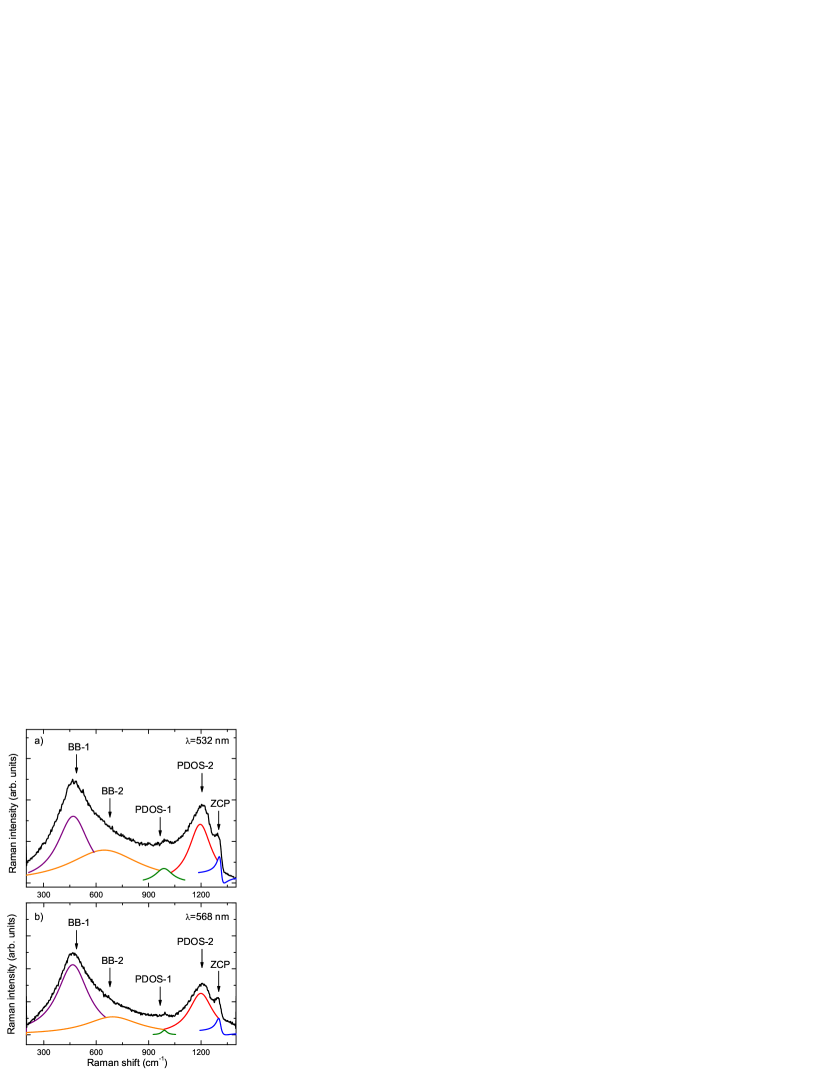
In Fig. 1, Raman spectra of heavily boron doped diamond (BDD) are depicted at and .
The Raman bands around cm-1 (denoted by BB-1 and BB-2 in Fig. 1), were assigned to boron dimers Bourgeois et al. (2006); Bernard et al. (2004); Sidorov and Ekimov (2010) and to clustered boron atoms Sidorov and Ekimov (2010).
Using first-principles calculations, boron dimers were found to form a stable structure upon heavy doping Bourgeois et al. (2006). The dimer-related vibrational and modes occur in our spectra as a broad feature.
As the low energy of the phonon mode would reflect unusually weak force constant between boron atoms, an alternative assignment is used as well in the literature Prawer and Nemanich (2004). Diamond irradiated with high-energy alpha particles showed the role of damage and defect concentration on Raman spectra Orwa et al. (2000). Amorphous diamond exhibits similar broad feature as heavily boron doped diamond.
Isotopic substitution did not give satisfying identification of the origin of the feature as both boron and carbon substitution gives shift on Raman spectra Sidorov and Ekimov (2010). The controversy of the interpretation might be resolved by regarding boron dimers to be point defects present in BDD in high concentration. The defect concentration correlates with the incorporated boron concentration, which reaches its maximum on the surface of the nanocrystals Liao et al. (1999). The inhomogeneous distribution of boron atoms in BDD Li et al. (2010) leads to the breaking of the Raman wavevector conservation rule and yields similar Raman spectra for BDD as for amorphous diamond.
The peak was fitted with the sum of two Lorentzian components (fit shown in Fig. 1), instead of a Lorentzian and a Gaussian component Bernard et al. (2004). The empirical relationship between the Raman shift of the lower Lorentzian component and the boron content () measured by secondary ion mass spectrometry (SIMS) found in Ref. Bernard et al. (2004) yields for the boron content in our sample. This value is in agreement with that obtained with Hall effect measurements in a similar material Gajewski et al. (2009). The approximate agreement found here and elsewhere May et al. (2008) further proves that the mode might be due to the high boron dimer concentration.
The Raman band around 1000 (PDOS-1) originates from the maximum of the phonon density of states of diamond. As discussed above, defects in the material make the otherwise forbidden states allowed Prawer et al. (1998). The Raman structure around 1200 cm-1 consists of two components: a Lorentzian like at 1210 cm-1 and another one with an asymmetric lineshape around 1300 cm-1. The 1210 cm-1 (PDOS-2) mode appears due to the presence of defects Sidorov and Ekimov (2010); Vlasov et al. (2008). In Ref. Pruvost and Deneuville (2001), the mode is assigned to boron-carbon complexes. It was reported that this peak exhibits Fano lineshape Ghodbane and Deneuville (2006). However, the mode does not exhibit asymmetry in our Raman spectra.
The zone center optical phonon of diamond, which occurs at 1332 cm-1 with cm-1 linewidth Liu et al. (2000), is shifted to 1300-1313 cm-1 in BDD and acquires a Fano lineshape due to the presence of free charge carriers Pruvost and Deneuville (2001); Gheeraert et al. (1993).
In Fig. 1, we show Fano lineshapes fitted on Raman spectra. The Fano lineshape Fano (1961) originates from the quantum interference between the zone center optical phonon and a continuum of electronic transitions around the same energy. It can be calculated as
| (1) |
where Int is the intensity of the Raman signal, and are respectively the real and imaginary parts of the self-energy in BDD after coupling between discrete phonon transition and a continuum of states:
| (2) |
and
| (3) |
Herein, is the density of states of the quasi-continuum, and are respectively real and imaginary part of the self-energy of the phonon in the undoped material. is the matrix element of the coupling between the two states and is the Hilbert transform of .
The asymmetry parameter, , reads
| (4) |
| (nm) | (cm-1) | (cm-1) | (meV) | |
|---|---|---|---|---|
| 532 | -1.4 | 1313 | 14.1 | -4.6 |
| 568 | -2.3 | 1307 | 15.7 | -7.2 |
| 514∗ | -1.7 | 1320 | 15.6 | -4.5 |
| 633∗ | -2.4 | 1316 | 14 | -5.8 |
where and are the Raman scattering amplitudes of the decoupled phonon and the electronic continuum Pruvost and Deneuville (2001); Cerdeira et al. (1973). If the electronic continuum disappears, and , the Fano formula becomes the usual Lorentzian curve.
Parameters of the Fano resonance lines are given in Table 1. Therein, is calculated for both wavelengths. Fano parameters from Ref. Pruvost and Deneuville (2001) for a (001) MPCVD sample with a slightly lower doping level are shown together with present experimental results. The lower doping level in Ref. Pruvost and Deneuville (2001) is confirmed by the higher resonant wavenumber, as the downshift is correlated with the boron incorporation Ushizawa et al. (1999). (Note that the boron content is not equivalent to the carrier concentration, as boron dimers present in the material do not contribute to free carrier concentration Bustarret et al. (2008).)
The negative sign of is in agreement with Raman measurements in the visible range Pruvost and Deneuville (2001); Wang et al. (2002). The positive value was calculated Cardona and Christiensen (1986). The negative values are given in theoretical calculations Calleja et al. (1978). The excitation energy, which is lower than the band-gap, contributes to positive .
The Raman scattering cross section increases with the excitation frequency as , where is the incident photon frequency. The Raman tensor of the decoupled phonon is expected to follow , while there is no similar relation for . is independent of the photon excitation wavelength, so might be expected to decrease with increasing incident wavelength. However, experimental data in Table 1 contradicts this expectation Pruvost and Deneuville (2001). In Table 1, there is no typical wavelength dependence of the values. This anomaly, which is not supported by UV excitation measurements Locher et al. (1995); Ghodbane and Deneuville (2006), demands further investigation both in visible and UV range. In Ref. Vlasov et al. (2008), the anomalous wavelength dependence of was explained by the presence of regions with very high boron concentration, which result in breaking of the wavevector conservation rule and a strong enhancement in as approaching the plasmon frequency in the near infrared.
In Ref. Pruvost and Deneuville (2001), was found to be small. is large, as the deformation potential was obtained experimentally 99.1 eV Calleja et al. (1978). The present results in Table 1 show low values for and yield an even stricter upper bound for .
IV Conclusions
In summary, we performed Raman measurements in heavily boron doped nanocrystalline diamond. The Raman mode around 500 cm-1 is assigned to point-defect boron dimers. The 1003 cm-1 and the 1210 cm-1 Raman modes are assigned to the phonon density of states. The 1210 cm-1 Raman mode does not exhibit Fano lineshape.
The Fano line of the zone-center phonon of diamond is significantly red-shifted and indicates significant asymmetry (). The Raman scattering amplitude of the decoupled phonon is small and it shows an anomalous wavelength dependence.
V Acknowledgements
Work supported by the ERC Grant Nr. ERC-259374-Sylo, and by the New Széchenyi Plan Nr. TÁMOP-4.2.2.B-10/1.2010-0009.
References
- Ferrari et al. (2006) A. C. Ferrari, J. C. Meyer, V. Scardaci, C. Casiraghi, M. Lazzeri, F. Mauri, S. Piscanec, D. Jiang, K. S. Novoselov, S. Roth, et al., Phys. Rev. Lett. 97, 187401 (2006).
- Dresselhaus et al. (2005) M. Dresselhaus, G. Dresselhaus, R. Saito, and A. Jorio, Phys. Rep. 409, 47 (2005).
- Prawer and Nemanich (2004) S. Prawer and R. Nemanich, Philos. T. Roy. Soc. A 362, 2537 (2004).
- Mandal et al. (2011) S. Mandal, T. Bautze, O. A. Williams, C. Naud, E. Bustarret, F. Omnès, P. Rodière, T. Meunier, C. Bäuerle, and L. Saminadayar, ACS Nano 5, 7144 (2011).
- Field and Field (1992) J. Field and J. Field, The Properties of natural and synthetic diamond (Academic Press, London, 1992).
- Ekimov et al. (2004) E. Ekimov, V. Sidorov, E. Bauer, N. Mel’nik, N. Curro, J. Thompson, and S. Stishov, Nature 428, 542 (2004).
- Bustarret et al. (2004) E. Bustarret, J. Kačmarčik, C. Marcenat, E. Gheeraert, C. Cytermann, J. Marcus, and T. Klein, Phys. Rev. Lett. 93, 237005 (2004).
- Takano et al. (2007) Y. Takano, T. Takenouchi, S. Ishii, S. Ueda, T. Okutsu, I. Sakaguchi, H. Umezawa, H. Kawarada, and M. Tachiki, Diam. Relat. Mater. 16, 911 (2007).
- Moussa and Cohen (2008) J. E. Moussa and M. L. Cohen, Phys. Rev. B 77, 064518 (2008).
- Mott (1968) N. Mott, J. Non-Cryst. Solids 1, 1 (1968).
- Gonon et al. (1995) P. Gonon, E. Gheeraert, A. Deneuville, F. Fontaine, L. Abello, and G. Lucazeau, J. Appl. Phys. 78, 7059 (1995).
- Klein et al. (2007) T. Klein, P. Achatz, J. Kacmarcik, C. Marcenat, F. Gustafsson, J. Marcus, E. Bustarret, J. Pernot, F. Omnes, B. E. Sernelius, et al., Phys. Rev. B 75, 165313 (2007).
- Bustarret et al. (2008) E. Bustarret, P. Achatz, B. Sacépé, C. Chapelier, C. Marcenat, L. Ortéga, and T. Klein, Philos. T. Roy. Soc. A 366, 267 (2008).
- Ushizawa et al. (1999) K. Ushizawa, G. Mikka N., K. Watanabe, I. Sakaguchi, Y. Sato, and T. Ando, J. Raman Spectrosc. 30, 957 (1999).
- Pruvost and Deneuville (2001) F. Pruvost and A. Deneuville, Diam. Relat. Mater. 10, 531 (2001).
- Gheeraert et al. (1993) E. Gheeraert, P. Gonon, A. Deneuville, L. Abello, and G. Lucazeau, Diam. Relat. Mater. 2, 742 (1993).
- Fano (1961) U. Fano, Phys. Rev. 124, 1866 (1961).
- Cerdeira et al. (1973) F. Cerdeira, T. A. Fjeldly, and M. Cardona, Phys. Rev. B 8, 4734 (1973).
- Ager et al. (1995) J. W. Ager, W. Walukiewicz, M. McCluskey, M. A. Plano, and M. I. Landstrass, Appl. Phys. Lett. 66, 616 (1995).
- Wang et al. (2002) Y. Wang, S. Lau, B. Tay, and X. Zhang, J. Appl. Phys. 92, 7253 (2002).
- Locher et al. (1995) R. Locher, J. Wagner, F. Fuchs, M. Maier, P. Gonon, and P. Koidl, Diam. Relat. Mater. 4, 678 (1995).
- Ghodbane and Deneuville (2006) S. Ghodbane and A. Deneuville, Diam. Relat. Mater. 15, 589 (2006).
- Hees et al. (2011) J. Hees, A. Kriele, and O. A. Williams, Chem. Phys. Lett. 509, 12 (2011).
- Gajewski et al. (2009) W. Gajewski, P. Achatz, O. A. Williams, K. Haenen, E. Bustarret, M. Stutzmann, and J. A. Garrido, Phys. Rev. B 79, 045206 (2009).
- Fábián et al. (2011a) G. Fábián, C. Kramberger, A. Friedrich, F. Simon, and T. Pichler, Rev. Sci. Instrum. 82 (2011a).
- Fábián et al. (2011b) G. Fábián, C. Kramberger, A. Friedrich, F. Simon, and T. Pichler, Phys. Status Solidi B 248, 2581 (2011b).
- Bourgeois et al. (2006) E. Bourgeois, E. Bustarret, P. Achatz, F. Omnès, and X. Blase, Phys. Rev. B 74, 094509 (2006).
- Bernard et al. (2004) M. Bernard, C. Baron, and A. Deneuville, Diam. Relat. Mater. 13, 896 (2004).
- Sidorov and Ekimov (2010) V. Sidorov and E. Ekimov, Diam. Relat. Mater. 19, 351 (2010).
- Orwa et al. (2000) J. O. Orwa, K. W. Nugent, D. N. Jamieson, and S. Prawer, Phys. Rev. B 62, 5461 (2000).
- Liao et al. (1999) C. Liao, Y. Wang, and S. Yang, Diam. Relat. Mater. 8, 1229 (1999).
- Li et al. (2010) H. Li, T. Zhang, L. Li, X. Lü, B. Li, Z. Jin, and G. Zou, J. Cryst. Growth 312, 1986 (2010).
- May et al. (2008) P. W. May, W. J. Ludlow, M. Hannaway, P. J. Heard, J. A. Smith, and K. N. Rosser, Diam. Relat. Mater. 17, 105 (2008).
- Prawer et al. (1998) S. Prawer, K. Nugent, and D. Jamieson, Diam. Relat. Mater. 7, 106 (1998).
- Vlasov et al. (2008) I. I. Vlasov, E. A. Ekimov, A. A. Basov, E. Goovaerts, and A. V. Zoteev, ArXiv e-prints (2008), eprint 0801.1611.
- Liu et al. (2000) M. S. Liu, L. A. Bursill, S. Prawer, and R. Beserman, Phys. Rev. B 61, 3391 (2000).
- Cardona and Christiensen (1986) M. Cardona and N. Christiensen, Solid State Commun. 58, 421 (1986).
- Calleja et al. (1978) J. M. Calleja, J. Kuhl, and M. Cardona, Phys. Rev. B 17, 876 (1978).