Van der Waals–Casimir–Polder interaction of an atom with a composite surface
Abstract
We study the dispersion interaction of the van der Waals and Casimir–Polder (vdW-CP) type between a neutral atom and the surface of a metal by allowing for nonlocal electrodynamics, i.e. electron diffusion. We consider two models: (i) bulk diffusion, and (ii) diffusion in a surface charge layer. In both cases the transition to a semiconductor is continuous as a function of the conductivity, unlike the case of a local model. The relevant parameter is the electric screening length and depends on the carrier diffusion constant. We find that for distances comparable to the screening length, vdW-CP data can distinguish between bulk and surface diffusion, hence it can be a sensitive probe for surface states.
pacs:
34.35.+a – interactions of atoms with surfaces; 31.30.jh – long-range QED interactions.I Introduction
Recent progress in the understanding of the van der Waals–Casimir–Polder (vdW-CP) force between an atom and a surface allows by now to distinguish surface properties with respect to charge transport. Data on the temperature and atom-surface distance dependence provide excellent tools for such analysis. In particular the experiments on fused silica harber have demonstrated a temperature dependence of the vdW-CP interaction. Fused silica is considered as a dilutely doped semiconductor that has a finite conductivity . The data was fitted successfully to the potential for a dielectric surface which differs from the one for a perfectly reflecting mirror, as considered by Casimir and Polder cp . In fact, since diverges at zero frequency, any nonzero conductivity will reproduce the perfect reflector result Klimchitskaya08 . It has been suggested to resolve this puzzle with the help of a nonlocal model of the electromagnetic response, where charge diffusion and screening become essential at low conductances Pitaevskii08 , although the approach was met with criticism comments-and-reply . In a related experiment on the (macroscopic) Casimir force between a gold-coated sphere and a single-crystal silicon membrane Chen2007 , the results are consistent with a dielectric behavior in its pristine form (ignoring the tail). The significant change in the charge carrier density after laser illumination leads to a metallic response in local form, again in agreement with Casimir force measurements. Nonlocal theories have been worked out to understand the crossover between these limits Pitaevskii08 ; Dalvit08 ; Svetovoy2008 , although experimental data favor a local description where the contribution of free charge carriers is omitted in the dielectric state Chen2007 ; comments-and-reply . For the discussion whether nonlocal electrodynamics may be applied to macroscopic Casimir interactions, and its consistency with thermodynamics, see Refs.Barash75 ; comments-and-reply ; comments-and-reply-Dalvit08 ; KlimchitskayaJPhysA2008 ; PitaevskiiLaserPhysics2009 .
The ability of probing charge transport may provide for an increased understanding of surface science by using the vdW-CP interaction as a probe. This viewpoint may be traced back to the seminal paper by Zaremba and Kohn Zaremba1976 where the van der Waals potential (neglecting retardation) was calculated with a microscopic description of the many-electron response of a metal. Their analysis yields an expression for the reference plane with respect to which the atom-surface distance is actually calculated. See Ref.Dobson2012 for a review of related methods. Dorofeyev Dorofeyev2007 analyzed the van der Waals (non-retarded) regime with the help of a nonlocal (-dependent) electromagnetic response based on the surface impedance work by Kliewer and Fuchs Kliewer1968 ; the electrons were assumed to reflect specularly from the inner surface.
In the present work, we compare two non-local models that can be understood as mesoscopic extensions of the work by Zaremba and Kohn: the first one allows for bulk diffusion as in Refs.Pitaevskii08 ; Dalvit08 , we denote it “continuous charge” (CC). In the non-retarded limit, this reduces to the Kliewer and Fuchs approach for a hydrodynamic dielectric function in the bulk. The model (ii) allows for diffusion only within a surface layer (“charge layer” or CL), the bulk charges responding with a local conductivity. Such composite surfaces with charges in the bulk and on the surface, are fairly common in metallic systems. These surfaces are either covered with adsorbates or nanostructures and can, e.g., be used as sensitive chemical sensors and biosensors homola , or are disordered with quantum well states at the surface varykhalov . Further motivation for a two-type charge model comes from studies of the anomalous heating of cold ions observed in miniaturized Paul traps that invoke surface charge fluctuations on the metallic electrodes Turchette00a ; Leibrandt07b ; Henkel08 ; Dubessy09 ; Daniilidis11 . Composite surfaces have also been explored regarding surface plasmons and lead to a wide range of dispersion relations, as observed in different systems, see Ref.Horovitz2012 and references therein.
The hallmark of the non-local theory is charge diffusion. In the CC model, it is described by the diffusion coefficient in the bulk, while describes surface diffusion in the CL. We identify a screening length for CC (cgs units)
| (1) |
where are the bulk conductivity and background dielectric constant, respectively (replace with in the CL model). As the atom-surface distance becomes comparable to the length scale , the vdW-CP interaction changes its behaviour. We consider different materials where can be compared with the other two important length scales of the vdW-CP potential: the radiation wavelength , being the atomic transition frequency, and the thermal photon wavelength at temperature . As common for electric dipole transitions in the visible range, we assume here , but explore otherwise the full range of distances. After defining the charge models (section II), we study in section III the case that is in the van der Waals (short distance) regime, , focusing on the case. In section IV, the length is in the Casimir-Polder (intermediate) regime, , while in section V we consider long distances where screening affects the Lifshitz (thermal) regime of the interaction. In all these cases we find that the crossover from the vdW-CP potential for a local conductor to a dielectric occurs at . In addition, the dispersion interaction is a good surface probe in the sense that the crossover is different in the CC and CL systems. This difference is particularly visible when the two limits, metallic and dielectric, are well separated. The relevant parameters are discussed in the conclusion.
II Model
II.1 Atom–surface interaction potentials
We use in this paper the general formulation of Wylie and Sipe Wylie1984 for the Casimir-Polder potential of an atom with a surface. Assuming the surface and the electromagnetic field in equilibrium at temperature , the free energy of interaction is given by
| (2) |
which is a sum over Matsubara frequencies along the imaginary frequency axis. The primed sum is taking the term with a factor . The atomic polarizability is given in Eq.(4) below, the retarded Green tensor is made explicit in Eqs.(6,7). In the limit , reduces to the interaction energy
| (3) |
This formulation applies for an atom in the ground state, for which the polarizability tensor is given by
| (4) |
where is the transition frequency between the ground state () and an excited state () with an electric dipole matrix elements and . We focus on a single resonance and assume rotational symmetry, so that and the polarizability is isotropic, .
The electromagnetic Green tensor in Eq.(2) provides the electric field radiated by a test dipole located at and oscillating with amplitude at frequency :
| (5) |
For a source outside a polarizable body, this electric field can be calculated within macroscopic electrodynamics (see, e.g., Ref.Wylie1984 ) and involves the reflection (or scattering) amplitudes of the body. It turns out that these amplitudes are sufficient to determine the Casimir-Polder interaction. The subtraction of the free-space part of the Green tensor (Lamb shift) is understood in the following. At a planar surface, only two principal polarizations are relevant, and the reflection amplitudes depend on frequency and a wave vector parallel to the surface . As we put in Eqs.(2, 3), the planar symmetry implies that the Green tensor is diagonal with elements Wylie1984 (cgs units)
| (6) | |||||
| (7) |
the element being identical to . The vacuum decay constant for a field mode with frequency and parallel wave vector is
| (8) |
with the root chosen such that and . The reflection amplitudes are collected in Table 1 for the different surface models considered in this paper. The general Eq.(2), valid for any , now takes the form
| (9) |
Let us briefly recall the assumptions behind the Wylie and Sipe approach Wylie1984 : the interaction energy is calculated in perturbation theory with respect to the atom-field coupling, starting from a well-defined atomic level (here, the ground state). The temperature provides Boltzmann weights for the excited states of the electromagnetic field, thus including the interaction with blackbody radiation and its modification by the surface. The thermal population of excited states of the atom is negligible provided the Bohr frequency is large enough, . Otherwise, a temperature-dependent polarizability should be used in Eqs.(2, 9). Finally, the surface response is worked out ignoring the presence of the atom and assuming a linear response of the surface to electromagnetic radiation, consistent with common practice in surface spectroscopy. By inspection of Eq.(9), one notes that wave vectors up to are relevant for the interaction potential. At distances much larger than the size of the unit cell, a macroscopic treatment of the surface response is therefore justified. There have been discussions what kind of electromagnetic response may be used consistently for atom-surface potentials and macroscopic Casimir interactions in general, see Refs.Barash75 ; comments-and-reply ; comments-and-reply-Dalvit08 ; KlimchitskayaJPhysA2008 ; PitaevskiiLaserPhysics2009 . The approach of Ref.Wylie1984 is based on the fluctuation-dissipation theorem Landau9 .
II.2 Surface response with charge diffusion
| local | hydrodynamic bulk charge (CC) | charge layer (CL) | |
|---|---|---|---|
Symbols used: The dielectric function is defined at (18) while is defined at (17). Spatial decay rates are for the vacuum , Eq.(8), for transverse fields in the medium with and for compressional charge waves with and .
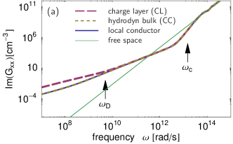
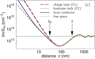
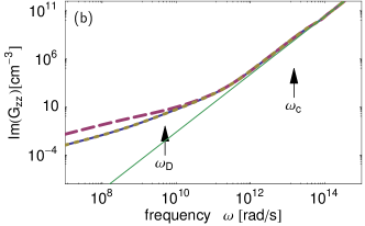
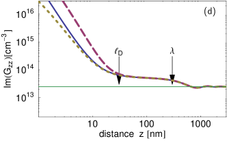
(right column) Distance dependence of the local mode density near a metallic surface, described by the same models as in the left column. Same parameters, except that the frequency is fixed to (near-infrared). The plots include the free space response, that leads to a constant limit at large distance (thin horizontal lines). The oscillations are due to partial standing waves formed above the surface. Diffusion length for these parameters: (left arrow); right arrow: reduced wavelength .
Surfaces covered with thin layers of strongly localized charges or adsorbates have been studied in much detail in surface physics. For a general theory of their electromagnetic response, see Refs.Sipe80 ; BedeauxVlieger . We consider here a model introduced in Ref.Henkel08 where the surface is covered by a charge sheet with a charge density (localized in the plane ). The details of the electromagnetic response are worked out in Appendix A. The sheet current in the layer responds by diffusion
| (10) |
where is the surface diffusion coefficient and a surface relaxation time. The gradient appearing here is parallel to the layer. A surface conductivity term proportional to is neglected, as justified for a small layer thickness, see Appendix A.3. Charge conservation yields
| (11) |
so that the bulk current just below the layer, , provides the influx into the surface layer. We take the bulk current response in the usual Ohmic form
| (12) |
where the Drude conductivity is with a scattering time . Eqs. (10,12) define the CL (charge layer) model.
The CC (continuous charge) model, in contrast, is defined by the bulk charge density that has a diffusion constant , i.e. Eq. (12) is replaced by
| (13) |
The (“additional”) boundary condition for the current is then , since there are no surface charges.
The resulting reflection amplitudes are summarized in Table 1 and more details on their derivation are given in Appendix A. One notes that the TE polarization is not affected by the composite structure of the surface. This can be understood from the fact that surface charges are created by electric fields perpendicular to the surface, which are absent in this polarization.
To illustrate the impact of the diffusive layer, we have calculated the local photonic mode density, i.e., the imaginary part of . This quantity can be measured from the spontaneous decay rate of an excited atom placed at or from the heating rate of an ion trapped near a surface Turchette00a ; Leibrandt07b ; Henkel08 ; Dubessy09 ; Daniilidis11 . The results shown in Fig.1 illustrate the enhancement of the mode density at low frequencies (below the characteristic scale left column). At large wave vectors (short distances, right column), there is a competition between additional modes (enhancing the mode density, CL model) and screening (reducing it, CC model). Note that for the parameters considered here the screening length is much smaller than the diffusion length ). An excited atom decays faster because diffusion along the surface broadens the field spot it creates, increasing the effective area where absorption takes place. Calculations of the Casimir (plate-plate) interaction between materials with a nonlocal electromagnetic response have revealed qualitatively similar trends (compare Refs.Esquivel04a ; Svetovoy06a to Ref.Contreras-Reyes05a ). The experimental data of Ref.Chen2007 are better described with a local rather than nonlocal theory, however, see Ref.KlimchitskayaJPhysA2008 and the discussion in Refs.MostepanenkoIJMPA2009 ; PitaevskiiLaserPhysics2009 .
III Van der Waals (nonretarded) regime
This regime corresponds to short distances where retardation is negligible
| (14) |
with a typical value for transitions in the visible range. The Van der Waals interaction follows a power law for a material with a local response (Drude metal or dielectric). We consider in this section the situation that the screening length (see Introduction) satisfies ; this corresponds to electron densities typical for metals.
We start from the zero-temperature expression for the interaction potential, combining Eqs.(3, 4, 6, 7):
where now . The dominant ranges of the integrals are around , due to the exponential, and , due to the polarizability . This allows to simplify Eq. (III) by taking and , so that for the CL model (see Table 1)
| (16) | |||||
The reflection amplitude involves a “surface dielectric function” given by (see Ref.Henkel08 and Appendix A)
| (17) |
where is the surface diffusion coefficient [see Eq.(10)]. The conventional Drude dielectric function (local), with a bulk relaxation time and a high-frequency asymptote , is
| (18) |
which happens to be the limiting form of Eq.(17) when . From the -dependence in , we identify the dimensionless ratio that defines the screening length consistent with the estimate (1) of the Introduction. For , the reflection amplitude in Eq.(16) recovers the local behaviour, while at very short distances, , the diffusive (nonlocal) term dominates. The latter case implies that the conductivity contribution is suppressed in Eq.(17), leaving only the background dielectric constant .
If , both limiting cases (conductor and dielectric) show a van der Waals interaction that follows the familiar power law, but with different coefficients. For the dielectric,
| (19) |
while the local Drude conductor gives Wylie1984
| (20) |
Here, is the surface plasmon frequency, and we have neglected Ohmic losses (i.e., ). The composite surface models with their nonlocal response give a van der Waals interaction that crosses over between these two limits (see Fig.3 below). This is similar to what has been analyzed at large distances by Pitaevskii Pitaevskii08 .
We focus here on the somewhat academic case of a simple free-electron metal ( ), where the nonlocal surface reponse changes even the exponent at short distances because the coefficient in Eq.(19) vanishes. To get insight into the small-distance behaviour, we expand the CL reflection coefficient at high momentum and get for
| (21) |
Note that the imaginary frequency drops out in this case and the suppression on scales shorter than the screening length . The integral in Eq.(16) can then be performed, and one gets for the simple result
| (22) |
instead of the power law. In Fig.2, we compare the exact evaluation of the van der Waals potential (III) (dashed curve) to the numerical integration over of the approximate reflection amplitude (21) (solid gray curve). One gets a good approximation over a wide range of non-retarded distances . Note how the non-local theory matches with the local conductor (solid blue curve) as .
A similar analysis for the CC model [Table 1] yields a screening length involving the bulk diffusion constant, and the approximate form
| (23) |
Despite the difference in the reflection amplitudes (21, 23), the short-distance asymptote turns out to be just a factor of one half smaller than Eq.(22) (upper solid gray curve in Fig.2). These results illustrate the dramatic impact of nonlocal electrodynamics on the van der Waals interaction. We expect them to apply qualitatively in materials where the background polarizability provided by bound electrons is relatively small. The coefficient in Eq.(19) is then nonzero, but weak and shifts the short-distance asymptotes of the CL and CC curves in Fig.2 below zero.
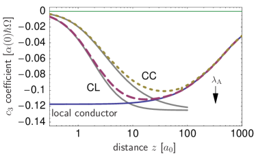
Parameters: DC conductivity (typical for Al), dielectric constant , electron scattering times , diffusion constants , atomic resonance wavelength (). For these parameters, the screening length is . The van der Waals interaction with a local Drude conductor gives a normalized value from Eq.(20). The CC/CL models show, at short distances, a much weaker interaction potential given in Eq.(22).
IV Casimir-Polder (retarded) regime
This regime corresponds to an intermediate range of distances,
| (24) |
where the thermal wavelength at . This range is characterized by the form for both dielectric and metallic surfaces with a local dielectric response.
For analytic expansions, we consider so that the -integral of Eq.(3) still applies. From the exponent , we read off the characteristic frequency that limits the -integration range to . In the CP regime (24), is much smaller than the atomic resonance , and we can expand the polarizability
| (25) |
The following discussion applies to a free-electron metal at high density where and .
IV.1 Good conductor
We then have the small parameter to simplify the reflection coefficients. It turns out that the impact of charge diffusion is very small in the Casimir-Polder regime: for the CL model, we find by inspection that the relevant dimensionless ratio is . We start with the zeroth order with respect to this ratio and expand in powers of
| (26) |
Performing the integrations, we get the familiar Casimir-Polder potential and next-order corrections
| (27) | |||||
where the incomplete Gamma function is . The limiting values of third term give a correction as and as .
Note that these approximations correspond to two inequivalent ways of implementing the perfect-conductor limit. The first case could be called “overdamped”, with a purely real conductivity. The penetration of transverse fields into the bulk then occurs by means of diffusion. The correction to the Casimir-Polder potential in Eq.(27) scales like where is the magnetic diffusion length at the characteristic frequency . In the second case, the conductivity is purely imaginary and, similar to a superconductor, the transverse field is screened from the bulk. The correction to the Casimir-Polder potential arises from the field penetrating a thin layer of the order of the plasma wavelength (also called London-Meissner penetration depth) , and scales like . The latter case has been studied, for example, in Ref.Bezerra08 , Eq.(37), and their result is recovered by the two correction terms in Eq.(27):
| (28) |
where is the first term in Eq.(27). This range of distances is quite narrow for the parameters of Fig.2, where .
Let us now extract the contribution due to the diffusive charge layer (CL model). To the first order in the surface diffusion coefficient , the correction to the local model can be worked out to be:
| (29) |
In the limiting case , , the integration gives a relative correction ; in the opposite limit, where the speed of sound characterizes the dispersion of longitudinal modes in the charge layer. The latter estimate illustrates that the correction brought about by the charge layer is negligible in the Casimir-Polder regime. A similar conclusion is reached for the continuous charge (CC) model; we omit the calculations for brevity. The numerical results from Fig.2 illustrate that both CL and CC models merge into the local description in the Casimir-Polder range .
IV.2 Semiconductor
Fig.3 shows numerical calculations of the interaction potential for a material with a conductivity typical for semiconductors. The characteristic length for screening is then much larger and falls into the Casimir-Polder range of the atom-surface potential. The data show that the CC and CL models interpolate between the limiting cases of a local Drude conductor and a non-conducting dielectric (where does not diverge at zero frequency). We have taken the relatively low value to amplify the difference between the dielectric and the conductor in the local limit: their difference scales with .
In Fig.3, we show the free energy of interaction calculated from the Matsubara sum (9). At distances beyond the thermal wavelength , the free energy follows a power law with a coefficient proportional to that we discuss in the following section. The difference between dielectric and Drude conductor arises, for these parameters, from the zeroth term in the Matsubara sum. This term is discussed in more detail in Sec.V. Indeed, in the other terms, the conductivity enters only in the ratio . At room temperature, this ratio can be neglected compared to the background dielectric constant provided the conductivity . This regime applies to a wide range of doped semi-conductors.
The van der Waals regime for this material is not described by Eq.(20) due to the low conductivity. Ignoring conductivity completely, Eq.(19) for a local dielectric gives a short-range coefficient with a value in the units of Fig.3: this corresponds well to the full calculation. We have checked that the small difference is actually due to relatively large deviations from the non-retarded approximation that was applied to derive Eq.(19). A similar situation occurred in Ref.Bostroem12 which discusses the Casimir force between two plates separated by a dielectric liquid.
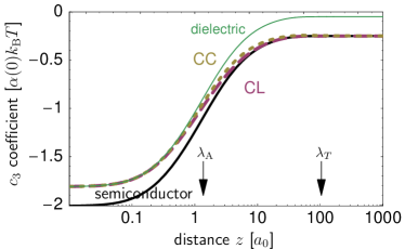
Parameters: background dielectric constant , DC conductivity (comparable to Ge), electron scattering time , diffusion constants , atomic resonance (wavelength ), Temperature (thermal wavelength ).
V Lifshitz (thermal) regime
This section deals with the long distance regime where the leading contribution to the atom-surface potential is given by the term in the Matsubara sum (9). The other terms are proportional to the exponentially small factor and can be neglected if the term is nonzero. A glance at Fig.3 illustrates that the thermal regime is already well borne out at due to the factor in the exponential.
The static term in the Matsubara sum has been the subject of much discussion in the field of dispersion interactions Geyer2005 ; Klimchitskaya2009 . To illustrate this, we give the limiting forms of the free energy in the thermal range for an ideal dielectric material
| (30) |
while for a conductor in the same limit
| (31) |
In fact, the latter result is obtained for any material with a nonzero conductivity: as , the former (dielectric) result is not obtained in a continuous manner Klimchitskaya08 . This is due to the static reflection coefficient which is equal to for any nonzero , while setting from the start for a pure dielectric, one gets . This difference between conductor and dielectric is also visible in the Casimir-Polder range shown in Fig.3. The discontinuity disappears only in the limit for the material parameters considered here.
This effect is actually an artefact of the description in terms of a local material response (conductivity, dielectric function). Using a hydrodynamic model similar to our CC, Pitaevskii has shown that the free energy shows a continuous cross-over between the limiting cases Eqs.(30, 31). We show now that the same is true for both CC and CL models considered here.
For the CC model, the first line of Eq.(9) can be written in terms of a dimensionless integral ()
| (32) | |||
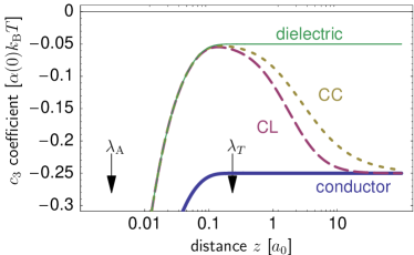
with the screening length of Eq.(1). We recover Pitaevskii’s result Pitaevskii08 by calculating from the diffusion coefficient of a non-degenerate electron gas. This leads to where is the carrier density in the conductor and the Bjerrum length (i.e., the distance where the Coulomb energy between two electrons becomes comparable to the thermal energy: ). A glance at Eq.(32) tells that the dielectric and metallic values of the reflection coefficient are smoothly interpolated as the ratio changes from zero to infinity. This is illustrated in Fig.4 (dotted line) where the coefficient of the power law is plotted vs .
The same qualitative behaviour is found in the CL model where the free energy takes the form
| (33) |
This is shown in dashed in Fig.4. The parameters chosen here are for a very poor conductivity (low carrier density) where the screening length is large enough to fall into the thermal range. This applies to dilutely doped semiconductors, or to the thermally excited conduction band of an intrinsic semiconductor.
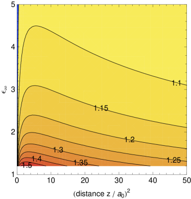
In Fig.5, we explore under which conditions the atom-surface interaction energy is most sensitive to the details of the surface charge response. This contour plot shows the ratio between the CL and CC results for the interaction energy in the thermal range, varying the distance and the background dielectric constant . The two models differ maximally in the cross over range , and for . This could have been expected from Eqs.(30, 31) because the dielectric and metallic limits (the two horizontal lines in Fig.4) are then most separated.
VI Discussion and conclusion
Any material with mobile charges is characterized by a screening length , and a local current-field relation (Ohm’s law) is necessarily limited to scales larger than . We have explored in this paper how screening at and below the surface influences the long-range van der Waals-Casimir-Polder (vdW-CP) interaction between an atom and the body. Our description may be termed ‘mesoscopic’ in the sense that the electronic response is collective in nature, but retains traces of ballistic carriers via the diffusion coefficient ( is a typical carrier velocity and the scattering mean free path). Two models for the electromagnetic response of the surface were studied in detail: a continuous charge distribution below the surface (CC) within a hydrodynamic approximation, and a thin charge layer (CL) with a diffusive response typical for, e.g., localized surface states. Both models provide a continuous crossover of the vdW-CP potential between two local limiting cases: a pure dielectric and a conducting medium, as the atom-surface distance goes through the range . The two limits can be distinguished from the zero-frequency limit of their dielectric functions and give different coefficients for the power laws that prevail at very short (van der Waals) and very large (thermal or Lifshitz) distances. Our calculations extend the picture proposed in Refs.Pitaevskii08 ; Dalvit08 to any distances, namely that the nonzero DC conductivity can be neglected if the atom-surface distance is shorter than the screening length [Eq.(1)].
The differences in the vdW-CP interaction may be used as a probe that can identify the type of charge transport in the (sub)surface region. The sensitivity of this probe is maximal when the screening length matches the atom-surface distance , particularly in the retarded range . The CC/CL difference is particularly large when the dielectric constant of bound carriers and background ions is close to . The reason is that the jump leads to a surface polarization charge that responds locally (not by diffusion) and is therefore masking the effect of either the CC or the CL. For transitions in the optical visible range, these favorable conditions correspond to which is indeed the achievable range of present experiments. A screening length occurs in a dilute semiconductor, which at room temperature is a non-degenerate electron system with . Hence we require a carrier density . This density can be achieved by dilute doping, as for fused silica Pitaevskii08 . One may also work with intrinsic semiconductors where the carriers are thermally excited with a density Dalvit08 ; ashcroft where is the gap. Hence, with and by varying the temperature, one can span a range around .
In conclusion, our two charge type models are representatives of a composite surface of a metal, with a nonlocal electromagnetic response due to charge transport in the bulk and at the surface. Such composite surfaces are fairly common corresponding to either surfaces covered with adsorbates or nanostructures, or to disordered surfaces with quantum well states. We have studied the Casimir-Polder interaction with such surfaces and have shown where this effect can be used as a sensitive probe of the surface type and its diffusive properties.
Acknowledgements. This research was supported by a grant from the German-Israeli Foundation for Scientific Research and Development (GIF). We thank H. Haakh for useful discussions and G. L. Klimchitskaya and V. M. Mostepanenko for comment.
Appendix A Surface response
A.1 Surface impedances
The calculation of the electromagnetic Green function proceeds by expanding the field created by a point source into Fourier components and finding reflection and transmission coefficients for each wave vector incident on the surface. With the wave vector in the -plane and the macroscopic body in the half-space , we have with . We consider separately two principal polarizations. In the TE-polarization, the electric field outside the surface is written in the form
| (34) |
where is the unit vector transverse to the plane of incidence. One gets the magnetic field from the Faraday equation: . The ratio between these two tangential fields, evaluated at , is the surface impedance and determines the reflection coefficient
| (35) |
In a local model for the body response, one has where the transmitted wave vector is , and the Fresnel formula is recovered.
In the TM-polarization the electric field vector is in the -plane, and Eq.(34) becomes
| (36) | |||||
This gives just above the surface. One defines impedance and reflection coefficient from the tangential (-) component of the electric field
| (37) |
Its local approximation is where is the bulk dielectric function.
A.2 Solving the reflection problem
We start to work out the electromagnetic response function in the TE-polarization. Within a local description of the bulk medium below the layer, one can work with a medium wave vector in the -plane, as defined after Eq.(35), with
| (38) |
An ansatz similar to Eq.(34) can be written down and augmented by a longitudinal part
| (39) | |||||
where the component of the longitudinal wave vector is as yet undetermined. From the Maxwell equations, the tangential component is continuous, and since it is zero above the layer [Eq.(34)], we find for the longitudinal amplitude. The field perpendicular to the surface is zero above and below the layer, hence the surface charge and the current density are zero from Eqs.(10, 11). The magnetic field is then continuous as well, and we get the local value for the surface impedance from
| (40) |
The reflection coefficient (35) takes the familiar form
| (41) |
In the TM-polarization, both transverse and longitudinal fields in the medium are relevant, as is well known Ford84 . The expansion (39) becomes
| (42) | |||||
The tangential field is continuous and becomes outside the layer
| (43) |
Due to the surface current density , the field has a jump, and one gets above the layer:
| (44) | |||||
We need to express and in terms of the transmitted amplitude : use charge conservation (11) and the continuity of the -component of the Ampère-Maxwell equation which links the jumps in (surface current) and in (surface charge). A straightforward calculation yields
| (45) |
and . Putting Eqs.(43)–(45) into Eq.(37), we thus find the impedance
| (46) |
where is the background dielectric function (excluding the conduction current).
A.3 Surface conductivity
If we model the charge layer as a film of thickness and conductivity , its integrated current density (parallel to the layer) has the form:
| (47) |
where the last term is the conduction current. Including this term in the surface response calculations we get reflection coefficients
| (48) | |||||
| (49) |
with the surface dielectric function being [cf. Eq.(17)]
| (50) |
We now identify under which conditions the terms proportional to are negligible in these expressions. For an order of magnitude estimate, we take and a layer thickness the atomic scale. Therefore we get from Eq.(50) the condition
| (51) |
An upper limit can be found easily at imaginary frequencies where , with the plasma frequency. Using the characteristic scales and in the integrals for the Casimir-Polder potential, the estimate (51) becomes
| (52) |
Hence we require the layer thickness to be much smaller than the smallest of the length scales distance , atomic transition wavelength and plasma wavelength . All these are conditions are well satisfied for . The surface dielectric functions and [Eqs.(50), (17)] and the reflection coefficients Eq.(48), Table 1 are equivalent.
As for the amplitude (49), we can neglect the surface conductivity term provided
| (53) |
As an estimate, this is equivalent to
| (54) |
The maximal value on the left hand side is , hence must be smaller than the plasma wavelength, as we found before in (52). In the limit of large , the difference in Eq.(49) becomes small, and the condition (53) must be replaced by
| (55) |
Estimating , we get which we also found in Eq.(52) above. For , also the amplitude is therefore not affected by the layer conductivity.
References
- (1) J. M. Obrecht, R. J. Wild, M. Antezza, L. P. Pitaevskii, S. Stringari, and E. A. Cornell, Phys. Rev. Lett. 98, 0632019 (2007).
- (2) H.B. Casimir, D. Polder, Phys. Rev. 73, 360 (1948)
- (3) G.L. Klimchitskaya, V.M. Mostepanenko, J. Phys. A 41, 312002(F) (2008)
- (4) L.P. Pitaevskii, Phys. Rev. Lett. 101, 163202 (2008)
- (5) B. Geyer and G. L. Klimchitskaya and U. Mohideen and V. M. Mostepanenko, Phys. Rev. Lett. 102, 189301 (2008); reply by L. P. Pitaevskii, Phys. Rev. Lett. 102, 189302 (2008).
- (6) F. Chen, G.L. Klimchitskaya, V.M. Mostepanenko, U. Mohideen, Phys. Rev. B 76(3), 035338 (2007)
- (7) D.A.R. Dalvit, S.K. Lamoreaux, Phys. Rev. Lett. 101, 163203 (2008)
- (8) V. B. Svetovoy, Phys. Rev. Lett. 101, 163603 (2008); erratum Phys. Rev. Lett. 102, 219903 (2009).
- (9) R. S. Decca & al, Phys. Rev. Lett. 102, 189303 (2009); reply by D. A. Dalvit and S. K. Lamoreaux, Phys. Rev. Lett. 102, 189304 (2009).
- (10) Y. S. Barash and V. L. Ginzburg, Sov. Phys. Usp. 18, 305 (1975).
- (11) G. L. Klimchitskaya, U. Mohideen, V. M. Mostepanenko, J. Phys. A 41, 432001 (2008).
- (12) V. M. Mostepanenko, R. S. Decca, E. Fischbach, B. Geyer, G. L. Klimchitskaya, D. E. Krause, D. Lopez, U. Mohideen, Int. J. Mod. Phys. A 24, 1721 (2009).
- (13) L. P. Pitaevskii, Las. Phys. 19, 632 (2009).
- (14) E. Zaremba, W. Kohn, Phys. Rev. B 13, 2270 (1976)
- (15) J.F. Dobson, T. Gould, J. Phys.: Condens. Matter 24(7), 073201 (2012)
- (16) I. Dorofeyev, Phys. Lett. A 363, 251 (2007)
- (17) K.L. Kliewer, R. Fuchs, Phys. Rev. 172(3), 607 (1968)
- (18) J. Homola, ed., Surface plasmon resonance based sensors (Springer, Berlin Heidelberg, 2006)
- (19) A. Varykhalov, A.M. Shikin, W. Gudat, P. Moras, C. Grazioli, C. Carbone, O. Rader, Phys. Rev. Lett. 95, 247601 (2005)
- (20) Q.A. Turchette, D. Kielpinski, B.E. King, D. Leibfried, D.M. Meekhof, C.J. Myatt, M.A. Rowe, C.A. Sackett, C.S. Wood, W.M. Itano et al., Phys. Rev. A 61, 063418 (2000)
- (21) D. Leibrandt, B. Yurke, R. Slusher, Quantum Inf. Comput. 7(1-2), 52 (2007)
- (22) C. Henkel, B. Horovitz, Phys. Rev. A 78, 042902 (2008)
- (23) R. Dubessy, T. Coudreau, L. Guidoni, Phys. Rev. A 80, 031402(R) (2009)
- (24) N. Daniilidis, S. Narayanan, S.A. Möller, R. Clark, T.E. Lee, P.J. Leek, A. Wallraff, S. Schulz, F. Schmidt-Kaler, H. Häffner, New J. Phys. 13, 013032 (2011)
- (25) B. Horovitz and C. Henkel, Europhys. Lett. 97, 57010 (2012)
- (26) J.M. Wylie and J.E. Sipe, Phys. Rev. A 30(3), 1185 (1984); 32(4), 2030 (1985).
- (27) E. M. Lifshitz and L. P. Pitaevskii, Statistical Physics (Part 2) (Pergamon, Oxford, 1980)
- (28) J. E. Sipe, Phys. Rev. B 22, 1589 (1980).
- (29) D. Bedeaux and J. Vlieger, Optical Properties of Surfaces. (World Scientific, Singapore, 2004)
- (30) R. Esquivel and V.B. Svetovoy, Phys. Rev. A 69, 062102 (2004).
- (31) V.B. Svetovoy and R. Esquivel, J. Phys. A 39, 6777 (2006).
- (32) A.M. Contreras-Reyes and W.L. Mochan, Phys. Rev. A 72, 034102 (2005).
- (33) V.B. Bezerra, G.L. Klimchitskaya, V.M. Mostepanenko, C. Romero, Phys. Rev. A 78, 042901 (2008)
- (34) M. Boström, B.E. Sernelius, I. Brevik, B.W. Ninham, Phys. Rev. A 85, 010701(R) (2012)
- (35) B. Geyer, G. L. Klimchitskaya, V. M. Mostepanenko, Phys. Rev. D 72, 085009 (2005).
- (36) G. L. Klimchitskaya, U. Mohideen, V. M. Mostepanenko, Rev. Mod. Phys. 81, 1827 (2009).
- (37) N.W. Ashcroft, N.D. Mermin, Solid State Physics (Saunders, Philadelphia, 1976)
- (38) G.W. Ford, W.H. Weber, Phys. Rep. 113, 195 (1984)