Raman spectroscopy of the interlayer shear mode in few-layer MoS2 flakes
Abstract
Single- and few-layer MoS2 has recently gained attention as an interesting new material system for opto-electronics. Here, we report on scanning Raman measurements on few-layer MoS2 flakes prepared by exfoliation. We observe a Raman mode corresponding to a rigid shearing oscillation of adjacent layers. This mode appears at very low Raman shifts between 20 and 30 cm-1. Its position strongly depends on the number of layers, which we independently determine using AFM measurements and investigation of the other characteristic Raman modes. Raman spectroscopy of the shear mode therefore is a useful tool to determine the number of layers for few-layer MoS2 flakes.
The tremendous growth of experimental research on graphene in the past few years stems, in part, from the simple exfoliation technique that allows for preparation of single- and few-layer flakes from bulk crystals. This technique is applicable to many layered crystal structures in which the binding energy between adjacent planes is much lower than the binding energy within a plane Novoselov et al. (2005). Among these layered structures, the dichalcogenide MoS2, which is used commercially, e.g., as a high-temperature dry lubricant, has attracted a lot of interest. It was recently shown to undergo a transition from indirect to direct-gap semiconductor when its thickness is reduced to a single layer Mak et al. (2010); Splendiani et al. (2010), leading to pronounced photoluminescence. This drastic change of the band structure has been investigated theoretically by a number of groups Lebègue and Eriksson (2009); Ellis et al. (2011); Kadantsev and Hawrylak (2012), and further calculations suggest the possibility of band structure engineering using strain Scalise et al. (2012). Low-temperature photoluminescence measurements revealed the presence of impurity-bound excitons in single-layer MoS2 flakes Korn et al. (2011), which can be suppressed in oxide-covered MoS2 Plechinger et al. (2012). The photocarrier lifetime in single-layer MoS2 is sufficiently short Korn et al. (2011) to make the material interesting for fast photodetectors, and a MoS2-based phototransistor was reported recently Yin et al. (2012). Room-temperature transistor operation with very large on/off ratio has been demonstrated for single MoS2 layers Radisavljevic et al. (2011). As in graphene, where research was initially focused on single layers and later expanded to study also bilayers and trilayers due to their different band structure, few-layer MoS2 flakes may be interesting for their transport properties: very recently, ambipolar transistor operation was shown in few-layer MoS2 Zhang et al. (2012). Both, chemical exfoliation Eda et al. (2011) and vapor phase growth techniques Zhan et al. (2012) have been demonstrated for MoS2, indicating the possibility of fabricating large-area thin films neccessary for potential applications. Similar to graphene, where Raman scattering has been used to determine, e.g., the layer thickness Ferrari et al. (2006) or the doping type and concentration Heydrich et al. (2010), Raman spectroscopy is a highly useful tool to map MoS2 flakes and to identify single layers Lee et al. (2010); Najmaei et al. (2012). This is facilitated by the fact that two characteristic Raman modes, A1g (out-of-plane optical vibration of the sulfur atoms) and E (in-plane optical vibration of Mo and S atoms), show opposite frequency dependence on the number of layers: the A1g mode increases its frequency with the flake thickness, while the E anomalously softens due to increased dielectric screening Molina-Sánchez and Wirtz (2011), so that the difference of the mode frequencies is characteristic for a certain number of layers. While many of the Raman modes of graphene and MoS2, or other dichalcogenides, are very different due to the different crystal structures, two modes are rather generic for layered crystal structures:
(1) a shear mode, in which adjacent layers rigidly oscillate relative to each other, with the oscillation amplitude lying in the layer plane. This mode was observed for, both, bulk graphite R. J. Nemanich and Solin (1975), and bulk MoS2 Verble et al. (1972). More recently it was detected in few-layer graphene Tan et al. (2012).
(2) a compression mode, in which adjacent layers oscillate rigidly, with the oscillation amplitude perpendicular to the layer plane. This mode was recently observed in few-layer graphene in a double resonant process in combination with an LO phonon Herziger et al. .
Here, we report on scanning Raman scattering measurements on MoS2 flakes. The MoS2 flakes were prepared using the transparent tape liftoff method well-established for graphene, from natural MoS2. A p-doped silicon wafer (specific resistivity Ohm cm, corresponding to degenerate doping) with 300 nm SiO2 layer and lithographically defined metal markers was used as a substrate. After initial characterization with an optical microscope, the samples were analyzed by Raman spectroscopy at room temperature. For this, we utilized a microscope setup, in which a 532 nm cw laser was coupled into a 100x microscope objective, which also collected the scattered light in backscattering geometry. The scattered light was recorded using a triple grating spectrometer equipped with a liquid-nitrogen-cooled charge-coupled device (CCD) sensor. The sample was mounted on a piezo-stepper table and scanned under the microscope. The spatial resolution of this setup is about 500 nm. For some of the Raman measurements, a cross-polarized backscattering geometry was used. Here, a polarizer was placed in front of the spectrometer so that only the scattered light with polarization perpendicular to the laser polarization was coupled into the spectrometer. In this scattering geometry, the spectrally broad background, which stems from inelastic light scattering of free carriers in the heavily p-doped Si substrate Chandrasekhar et al. (1980), is suppressed and allows us to obtain Raman spectra very close to the laser line.
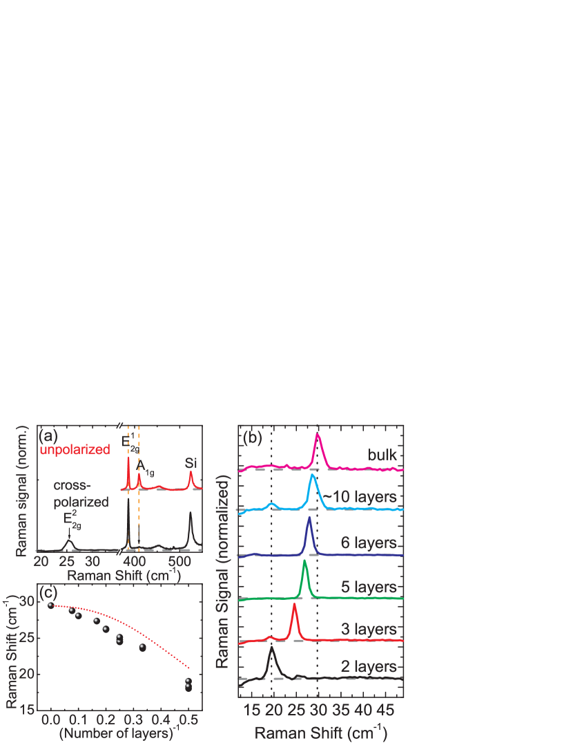
First, we discuss the typical Raman spectra observed in our samples. Figure 1 (a) shows two Raman spectra collected on a three-layer area of a flake. The top spectrum is recorded without a polarizer in front of the spectrometer, while the bottom spectrum is recorded in cross-polarized geometry, as described above. Due to the large and spectrally broad background caused by the silicon free-carrier scattering, the unpolarized spectrum is only recorded in a spectral range starting at 200 cm-1 with respect to the laser line, while the cross-polarized spectrum is collected in a range starting at 10 cm-1. In the unpolarized spectrum, we note the two characteristic Raman modes E (386.1 cm-1) and A1g (409.7 cm-1), with a frequency difference of 23.6 cm-1 as expected for three layers Lee et al. (2010). By contrast, in the cross-polarized spectrum, the A1g mode is almost completely suppressed, while the E mode remains visible. Additionally, in the cross-polarized spectrum, we observe a low-frequency mode at 25.3 cm-1, which we associate with the E interlayer shear mode. The main focus of this manuscript is the study of its frequency dependence on the number of MoS2 layers.
Our results are summarized in Figure 1(b): it shows normalized shear mode spectra obtained from MoS2 flakes of different thickness. The number of layers was determined independently, by, both, atomic force microscopy (AFM) measurements (see below), and investigation of the A1g - E frequency difference. We clearly observe that the shear mode shifts from below 20 cm-1 for a bilayer to about 30 cm-1 for bulk-like flakes, a very large relative shift of more than 50 percent. In Figure 1(c), we plot the shear mode positions extracted for 16 different flake areas as a function of (number of layers)-1. Multiple data points for a given thickness stem from measurements on different flakes. For comparison, we have calculated the expected mode position as a function of (number of layers)-1 as predicted in ref. Tan et al., 2012 using a linear chain model with fixed interlayer coupling strength. Here, we have used our measured value for the shear mode frequency in bulk as the only parameter. We clearly see that our experimental values show a more pronounced shift than expected using the linear chain model. Two factors may contribute to this difference: (a) we have to assume that, since all experiments were carried out under ambient conditions, the topmost layer of the MoS2 flake is partially covered with adsorbates, effectively increasing the mass per unit area. (b) our flakes are not free-standing, but deposited on a SiO2 substrate, therefore, the bottom layer will experience a weak van der Waals interaction with the substrate, which would act as an additional spring constant in the linear chain model.
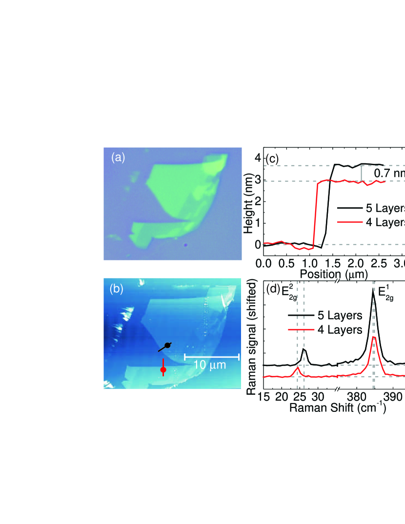
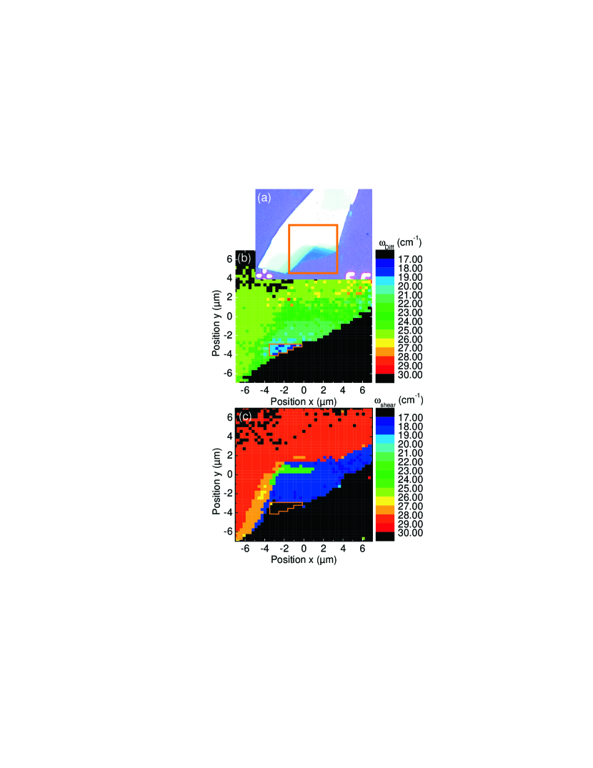
Figure 2 demonstrates the process of establishing the relation between shear mode position and number of layers in more detail. Utilizing flakes with large areas of uniform height, determined by optical microscopy, such as the one shown in Fig. 2(a), we determine the thickness of these areas by extracting height traces from AFM images. Raman spectra are then recorded at points on the flake for which the height is known. In Fig. 2(b), the AFM image corresponding to Fig. 2(a) is shown. The two colored lines indicate the position of the AFM line traces leading from the substrate to the flake shown in Fig. 2(c). From these traces, using the thickness of a single MoS2 layer of 0.7 nm, we find that the black trace corresponds to a step height of 5 layers, while the red trace corresponds to 4 layers. Raman spectra collected on these areas of the flake (Fig. 2(d)) demonstrate the large blueshift of the shear mode (about 1.8 cm-1), which is clearly visible in the data and also easy to determine using an automated fitting routine. By comparison, the E mode only shows a weak redshift (about 0.5 cm-1), so that even though the spectrally integrated intensity of this mode is about 8 times higher than that of the shear mode for a 5-layer region, the shear mode allows for easier discrimination of the number of layers.
The large relative shift of the interlayer shear mode can be used to efficiently map few-layer MoS2 flakes by using the shear mode position. One example is shown in Figure 3. The few-layer flake shown in Fig. 3(a) was scanned in the region marked by the square using the Raman microscope with a step size of 300 nm. The collected spectra were analyzed using an automated fit routine, which determines the peak positions of the A1g, E and E modes as a function of position. From this data, false color plots were generated. In Fig. 3(b), we plot the frequency difference A1g - E as a function of position. From the frequency difference we can clearly identify regions of different thickness, including a small monolayer area, which shows a frequency difference of about 18 cm-1 and is marked with a solid outline. Naturally, there is no shear mode signal in this region in Fig. 3(c), where we plot the shear mode frequency as a function of position. Comparing the contrast of the two false color images, where we have used the same false color scale, we immediately notice that the shear mode image shows much more well-defined transitions between regions of different thickness and easily allows to identify, e.g., a small trilayer region (green color) within the larger bilayer area (blue color), and a transition from 6 layers (dark yellow color) to about 10 layers (orange color), which are hard to discern from the frequency difference image.
In conclusion, we have used scanning Raman spectroscopy to study the interlayer shear mode in few-layer MoS2 flakes. We observe a large frequency shift of the shear mode to higher energies with increasing number of layers. This large shift allows us to precisely map the layer thickness in few-layer MoS2 flakes. The authors gratefully acknowledge financial support by the DFG via SFB689, SPP 1285 and GRK 1570 as well as fruitful discussion with L. Wirtz, A. Molina-Sánchez, J. Maultsch and N. Scheuschner.
References
- Novoselov et al. (2005) K. S. Novoselov, D. Jiang, F. Schedin, T. J. Booth, V. V. Khotkevich, S. V. Morozov, and A. K. Geim, Proc. Natl. Acad. Sci. U.S.A. 102, 10451 (2005).
- Mak et al. (2010) K. F. Mak, C. Lee, J. Hone, J. Shan, and T. F. Heinz, Phys. Rev. Lett. 105, 136805 (2010).
- Splendiani et al. (2010) A. Splendiani, L. Sun, Y. Zhang, T. Li, J. Kim, C.-Y. Chim, G. Galli, and F. Wang, Nano Letters 10, 1271 (2010).
- Lebègue and Eriksson (2009) S. Lebègue and O. Eriksson, Phys. Rev. B 79, 115409 (2009).
- Ellis et al. (2011) J. K. Ellis, M. J. Lucero, and G. E. Scuseria, Appl. Phys. Lett. 99, 261908 (2011).
- Kadantsev and Hawrylak (2012) E. S. Kadantsev and P. Hawrylak, Solid State Communications 152, 909 (2012).
- Scalise et al. (2012) E. Scalise, M. Houssa, G. Pourtois, V. Afanas ev, and A. Stesmans, Nano Research 5, 43 (2012).
- Korn et al. (2011) T. Korn, S. Heydrich, M. Hirmer, J. Schmutzler, and C. Schüller, Appl. Phys. Lett. 99, 102109 (2011).
- Plechinger et al. (2012) G. Plechinger, F.-X. Schrettenbrunner, J. Eroms, D. Weiss, C. Schüller, and T. Korn, physica status solidi (RRL) Rapid Research Letters 6, 126 (2012).
- Yin et al. (2012) Z. Yin, H. Li, H. Li, L. Jiang, Y. Shi, Y. Sun, G. Lu, Q. Zhang, X. Chen, and H. Zhang, ACS Nano 6, 74 (2012).
- Radisavljevic et al. (2011) B. Radisavljevic, A. Radenovic, J. Brivio, V. Giacometti, and A. Kis, Nature nanotech. 6, 147 (2011).
- Zhang et al. (2012) Y. Zhang, J. Ye, Y. Matsuhashi, and Y. Iwasa, Nano Letters 12, 1136 (2012).
- Eda et al. (2011) G. Eda, H. Yamaguchi, D. Voiry, T. Fujita, M. Chen, and M. Chhowalla, Nano Letters 11, 5111 (2011).
- Zhan et al. (2012) Y. Zhan, Z. Liu, S. Najmaei, P. M. Ajayan, and J. Lou, Small 8, 966 (2012).
- Ferrari et al. (2006) A. C. Ferrari, J. C. Meyer, V. Scardaci, C. Casiraghi, M. Lazzeri, F. Mauri, S. Piscanec, D. Jiang, K. S. Novoselov, S. Roth, et al., Phys. Rev. Lett. 97, 187401 (2006).
- Heydrich et al. (2010) S. Heydrich, M. Hirmer, C. Preis, T. Korn, J. Eroms, D. Weiss, and C. Schüller, Appl. Phys. Lett. 97, 043113 (2010).
- Lee et al. (2010) C. Lee, H. Yan, L. E. Brus, T. F. Heinz, J. Hone, and S. Ryu, ACS Nano 4, 2695 (2010).
- Najmaei et al. (2012) S. Najmaei, Z. Liu, P. M. Ajayan, and J. Lou, Appl. Phys. Lett. 100, 013106 (2012).
- Molina-Sánchez and Wirtz (2011) A. Molina-Sánchez and L. Wirtz, Phys. Rev. B 84, 155413 (2011).
- R. J. Nemanich and Solin (1975) G. L. R. J. Nemanich and S. A. Solin, in Proceedings of the International Conference on Lattice Dynamics, edited by M. Balkanski (Flammarion, 1975).
- Verble et al. (1972) J. Verble, T. Wietling, and P. Reed, Solid State Communications 11, 941 (1972).
- Tan et al. (2012) P. H. Tan, W. P. Han, W. J. Zhao, Z. H. Wu, K. Chang, H. Wang, Y. F. Wang, N. Bonini, N. Marzari, N. Pugno, et al., Nature Materials 11, 294 (2012).
- (23) F. Herziger, P. May, and J. Maultzsch, arXiv:1203.6043v2.
- Chandrasekhar et al. (1980) M. Chandrasekhar, U. Rössler, and M. Cardona, Phys. Rev. B 22, 761 (1980).