TRANSISTOR AS A RECTIFIER
Abstract
Transistor is a three terminal semiconductor device normally used as an amplifier or as a switch.
Here the alternating current(a.c) rectifying property of the transistor is considered. The ordinary
silicon diode exhibits a voltage drop of 0.6V across its terminals. In this article it is shown
that the transistor can be used to build a diode or rectify low current a.c(mA) with a voltage
drop of 0.03V. This voltage is 20 times smaller than the silicon diode. The article gives the
half-wave and full-wave transistor rectifier configurations along with some applications to justify
their usefulness.
1 Introduction
Rectification of a.c is normally carried out using silicon diodes(Kasatkin & Nemtsov 1986). The
silicon diode exhibits a voltage drop of 0.6V across its terminals when forward biased. This
0.6V is very small voltage if one wants to rectify voltages like 10V or 100V and hence the voltage
drop across the diode can be neglected. The diode for all practical purposes is considered to conduct
freely in one direction and completely non-conducting in the other direction(reverse bias). However
if one needs to rectify a.c of amplitude 1V, the 0.6V across the silicon diode forms a large
fraction(60%). Essentially the silicon diode cannot be used to rectify low voltage a.c(1V) if
one is interested in recovering the complete or almost complete(90%) waveform of the signal. In this
article the possibility of using a transistor as a rectifier(Pookaiyaudom et.al) is explored. It is
seen that the transistor rectifier exhibits a voltage drop of 0.03V or in other words it forms a diode
with this voltage drop. This voltage is 20 times smaller compared to the silicon diode and 5 times
smaller compared to the schottky diode(0.15V). Thus the transistor rectifier can be used to rectify
a.c as low as 10 times the voltage drop across it, 300mV. This article gives half-wave and full-wave
configurations of the transistor rectifier as shown in Figures 1 and 2 respectively.
2 The Transistor Rectifier


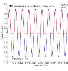
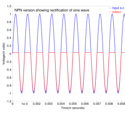
Rectification of alternating current with a single transistor has been considered. This simple circuit consisting of a transistor, a biasing diode and a few resistors can rectify a.c as low as 0.3V or even smaller. The rectification can be for positive half cycle or negative half cycle depending on the type of transistor(pnp/npn respectively) chosen. The schematic circuit of the rectifier is as shown in Figure-1. The quiescent forward biasing(Kasatkin & Nemtsov 1986) of the base-emitter junction of the transistors is taken care by the voltage drop across the silicon diodes(1N4148) in the side arms. The base-emitter junction of the silicon transistor and the silicon diode being similar the voltage drops across them are also more or less equal. The a.c to be rectified is introduced in the emitter circuit as shown in the Figure-1. Under these conditions any low negative voltage(NPN-version) appearing at the emitter would set up an emitter current which would mostly flow to the collector. However a small voltage drop(0.03V) across collector and emitter of the transistor is required to maintain this current. Essentially any additional voltage in the emitter circuit other than the balanced out voltage drops of the silicon diode and the base-emitter junction will be transfered to the collector circuit dropping across the load RL, as most of the emitter current flows to the collector. The Figure-1 shows both types of rectifiers which can rectify either the negative phase or the positive phase of the a.c signal. A full wave bridge rectifier using four transistors is shown in Figure-2. The results of computer simulation are shown in Figure-3. During the opposite phase i.e positive voltage w.r.t ground for NPN-version the base-emitter junction would be reverse biased however the base-collector junction is forward biased with the voltage drop across the biasing diode which is insufficient to setup a current through RL. Thus the circuit behaves as a rectifier passing only one phase of the a.c. The following appendix gives analysis and applications of the transistor rectifier.
Appendix A Analysis of the Rectifier
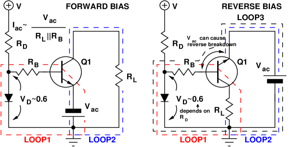
The forward bias and reverse bias operation of the NPN transistor rectifier are understood as shown in Figure 4. During forward bias(left figure) the voltage drop across the biasing diode V0.6V supplies the necessary base-emitter voltage drop for Q1. The negative voltage Vac w.r.t ground during this phase sees the LOOP1 and a current Vac/RB should flow through RB. This causes a voltage drop of Vac across RB. It is assumed that Vac/RB is drawn from the biasing diode’s(assuming RD is sufficiently low, however if RD is high then current through RB can be lower) current which can only cause a small change in its voltage drop as per its I-V characteristics. Vac also sets up current Vac/RL in the load resistor. If Vac is further increased it can even lead to reversing the voltage drop across the biasing diode(impedance : Vac(RD+RB)/(Vac+V) RL). However the upper limit on Vac is set by the reverse break down of BE junction (loop 3)which would be unfavourable for the life of the transistor. Further the value of RD plays a role in the reverse leakage current which is seen as a small constant voltage during the cutoff phase of ac(Figure 3). Smaller the value of RD higher is the voltage drop across biasing diode and more will be the leakage. The same is true for RB as well, however RB also plays a role in impedance seen by Vac. During reverse bias(Figure 4, right) the configuration is similar to that of a voltage follower however with the emitter replacing the collector and viceversa. Under this condition the voltage drop across the biasing diode is just sufficient to supply the BC junction forward biasing and not much is left for the voltage drop across RL if a current starts flowing through it. However a weak current can still flow through RL which depends on the voltage drop across the diode and in turn on the value of RD. This leakage is seen in Figure 3 as a small constant voltage few 10mV. The following sections give applications of the transistor rectifier.
A.1 Small signal AC voltmeter


The half wave rectifier in Figure 1 can be used to build a simple a.c voltmeter(Figure 6) which can measure a.c voltages
as low as 0.3V which using conventional 600mV voltage drop silicon diode is not possible, however one can still use
a schottky diode(150mV). The transistor gives a much smaller(5 times) voltage drop across its CE terminals and acts
as a diode with 30mV voltage drop. The schematic circuit diagram of the a.c voltmeter is as shown in Figure 5.
A.2 Inductance meter
The half wave transistor rectifier configuration can be used to build a L-R based inductance meter as shown in Figure 5 right. It is basically a modification of the half wave rectifier which includes appropriate electronic switching to drive the L-R circuit to a certain current and then allow it to decay unhindered through the transistor rectifier, however simultaneously measuring the current in the collector circuit. The transistor has the property of transfering a current from a lower resistance circuit(base-emitter) into a higher resistance circuit(base-collector). This property has been exploited here to measure inductance. By using a series L-R circuit in the emitter in place of the a.c voltage source it is possible to let a current carrying L-R circuit decay completely. At the same time this current can be measured without hindering the decay process in the L-R circuit. This is sufficiently warranted by the property of the transistor, for which it also derives its name! Transient analysis(Figure 6) of L-R circuit shows that, if in a certain time toff the L-R circuit’s current reduces to sufficiently low value say 5% or even less then for a period toff the average current is directly proportional to the value of the inductance. This is justified as, higher the value of inductance higher is the energy stored(=0.5LI2), for a given current. We can as well include another constant ton with toff without any loss of proportionality. During ton (transistor on time) the inductor is driven to a maximum current i0(VS-0.6)/R using proper switching circuitry. The plan to measure inductance is to first drive the L-R circuit to a maximum current i0 during the time ton. For the period ton the current through the meter is cutoff using the switch S4. Switch S3 opens to the +ve of the supply, S2 biases the transistor by connecting to +ve of the supply and S1 is off. The current through the L-R circuit evolves as a standard L-R circuit connected to a source of voltage VS-0.6 and at the end of ton would have almost reached the maximum allowed current through the resistor R, i.e i0. These waveforms have been shown in detail in Figure 6. The periods ton & toff (transistor rectifier time) should be kept as close as possible (i.e equal). During toff the switches S2 and S3 are off and S1 and S4 are on. The current in the inductor now decays through the half wave rectifier. Since the transistor half wave rectifier is near to an ideal rectifier the decay loop appears essentially as an unhindered closed path to the L-R circuit. A tiny portion of the L-R current flows through the base but does not affect the inductance measurement seriously due to its negligible magnitude. Majority of the emitter current flows to the collector through the meter. As has been shown in the following discussion the average value of this is proportional to the inductance L. At the end of toff the current through the inductor would have decayed to almost zero value. The end result of the analysis of the inductance meter is contained in the following equation.
| (1) |
Where Rcoil(in k) is the coil resistance of the inductor LX under measurement. This has to be
measured using a resistance meter and is seriously applicable if LX has appreciable coil-resistance. Lread is the
value indicated by the inductance meter. The following discussion considers ton and toff phases and quantifies
various transients and derives the above equation.
First the evolution of charging current through the L-R circuit is considered. The magnitude of current at a time t in the L-R circuit when a potential difference exists across it is,
| (2) |
where i0( (VS - 0.6)/R )is the maximum current acheived at time t = . By considering the values of the components associated with NE555 we see that ton 20s when set for measuring a maximum inductance of 5mH. For this setting the maximum value of R/L that is possible is 2500/0.005 = 500000. So we see that at t = ton the exponential term in (1) is almost 0 as (Rton/LX) = 10. This means i = i0 at t = ton.
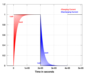
Next we consider the decay or discharge of current during toff . The current at time t in the L-R circuit once it starts decay is given by,
| (3) |
Since toff ton we see from the previous argument that i = 0 at t = toff. The plots of evolution/decay
of currents in the L-R circuit have been shown in Figure 6.
The timing diagram(Figure 6) clearly indicates that the current at the end of ton would have reached the maximum value or it would have decayed to 0 at the end of toff. So the average current through the meter assuming that the emitter current almost flows to the collector can be calculated as,
| (4) |
| (5) |
We see that the average current is directly proportional to the value of the inductance LX . Since ton toff
by the choice of R1 and R2 for NE555 astable [6], to measure values of inductances over a wide range
it is sufficient to change the timing capacitor associated with NE555 as this would proportionally increase (ton + toff) leaving
iavg unaltered.
To double the range of inductance measurement the value of this capacitor has to be simply doubled. Figure 5 shows the switching
arrangement that changes the range in steps of decades.
The inductor will also have an associated resistance with it which depends on the length/thickness of the wire. This can be accounted by modifying (4) as,
| (6) |
| (7) |
which is essentially multiplying the actual inductance by the factor (R/(R+RLx))2 . The manipulation in (5) is that due to the introduction of extra resistance RLx with LX the peak current to which the inductor is driven has reduced from i0 to i0R/(R+RLx). Next in the denominator R has to be replaced by (R+RLx). To rewrite and retain the form of (5) we throw an extra R in the numerator and denominator and rearrange into (6). RLx can be measured separately using a resistance meter. R is known to be 2.5k as per this design. It should be noted that R can be changed to 5k resulting in the modified range of 0-10mH instead of 0-5mH. The current evolution plots would still be the same with 5mH curve indicating the one for 10mH, but the peak current i0 would be halved. Further R may have to be calibrated slightly to get the right value of inductance. The actual inductance is obtained as the observed inductance multiplied by the inverse of the above mentioned factor i.e, ((R+RLx)/R)2. For example if R=2.5k as in our case we have,
| (8) |
where RLx is in k. Lactual is the true inductance of the test inductor and
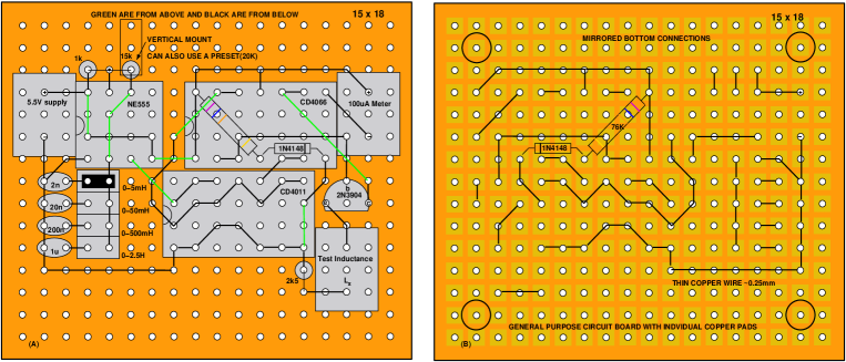
Lread is that shown by the meter. Figure 7 shows a circuit layout to help the reader build the instrument.
Actual performance of the instrument can be seen at http://youtu.be/Vyd84HvYhyo and http://youtu.be/E7cgomOn5pQ
References
- [1] Baddi R., Use a transistor and an ammeter to measure inductance, Design Ideas, EDN, April 05, 2012 .
- [2] http://en.wikipedia.org/wiki/Schottky_diode
- [3] Kasatkin A.S., Nemtsov M.V., Electrical Engineering, Mir Publishers, pp 260(5).
- [4] Pookaiyaudom S., Watanachaiprateep C. And Dejhan K., A Single Transistor Full-Wave Rectifier., 1979, Vol 67, Proceedings of the IEEE.
- [5] www.ti.com/product/cd4066b?CMP=AFC-conv_SF_SEP.
- [6] www.ti.com/product/ne555b?CMP=AFC-conv_SF_SEP or www.datasheetarchive.com.