Efficient quantum transport simulation for bulk graphene heterojunctions
Abstract
The quantum transport formalism based on tight-binding models is known to be powerful in dealing with a wide range of open physical systems subject to external driving forces but is, at the same time, limited by the memory requirement’s increasing with the number of atomic sites in the scattering region. Here we demonstrate how to achieve an accurate simulation of quantum transport feasible for experimentally sized bulk graphene heterojunctions at a strongly reduced computational cost. Without free tuning parameters, we show excellent agreement with a recent experiment on Klein backscattering [A. F. Young and P. Kim, Nature Phys. 5, 222 (2009)].
pacs:
72.80.Vp,73.23.Ad,73.40.Gk,72.10.BgI Introduction
Electronic transport is one of the important fields among the increasing number of fundamental studiesCastro Neto et al. (2009); Das Sarma et al. (2011) of graphene, a one-atom-thick carbon honeycomb lattice.Novoselov et al. (2004) Due to the gapless and chiral nature of its electronic structure, graphene exhibits energy dispersions linear in momentum, the transport carriers behave like massless Dirac fermions, and the properties based on Schrödinger wave mechanics in semiconductor physics have to be retreated by Dirac-type physics in graphene. Tunneling across pn and pnp junctions is perhaps the most popular example that shows how different the charge carriers behave, compared to semiconductor heterostructures. By solving the Dirac equation, perfect transmission at normal incidence across a potential stepCheianov and Fal’ko (2006) as well as a potential barrierKatsnelson et al. (2006) was shown for monolayer graphene. This mimicks the Klein paradox in quantum electrodynamics Klein (1929) and was later referred to as Klein tunneling,Beenakker (2008); Allain and Fuchs (2011) which attracted both experimentalHuard et al. (2007); Williams et al. (2007); Özyilmaz et al. (2007); Liu et al. (2008); Gorbachev et al. (2008); Stander et al. (2009); Young and Kim (2009); Nam et al. (2011) and further theoreticalZhang and Fogler (2008); Shytov et al. (2008); Gorbachev et al. (2008); Low et al. (2009); Yamakage et al. (2009); Low and Appenzeller (2009); Rossi et al. (2010); Ramezani Masir et al. (2010); Liu et al. (2012) investigations.
The Dirac theory, an effective approach valid only for low-energy excitations, generally serves as a starting point for theoretical studies of transport in graphene and can often provide analytical results to capture basic physical insights for certain problems with simplified system geometries. For further considerations, such as to maintain the lattice information on graphene or to account for complicated geometries and more realistic factors, one has to resort to more advanced theoretical models. The tight-binding model (TBM), a commonly used semiemperical approach for electronic structure calculations in solid state physics,Grosso and Parravicini (2000) allows for consideration of more complete band information on graphene at a low computational cost. The combination of the TBM with nonequilibrium Green’s function approaches forms the modern quantum transport formalism,Datta (1995) which is able to deal with a wide range of conductors composed of a scattering region and external leads with or without bias.
The description of the graphene scattering region of interest, however, requires a TBM Hamiltonian matrix,
| (1) |
whose matrix size depends on the involved number of atomic sites and therefore imposes a computational limit when addressing realistic experimental system sizes. This is partly the reason why many quantum transport studies address graphene “nanoribbons” rather than large-area graphene. The notation in Eq. (1) is described as follows: () is the nearest (next nearest) neighbor hopping parameter, is the local potential energy at site , () creates (annihilates) a charge carrier at the th site, and the summation () runs over all and site indices that are nearest (next nearest) to each other within the scattering region.
Typical sizes of graphene flakes for experimental transport investigations amount to a few microns by a few microns, but even a graphene flake contains roughly atoms, leading to a spinless single-orbital TBM Hamiltonian matrix of more than elements that requires an exceeding memory and hence an unreasonable computation burden. TBM-based quantum transport for bulk materials therefore requires further improvements to overcome the issue of the limited scattering region size. In this paper, we demonstrate how an accurate TBM-based transport calculation for bulk graphene heterojunctions can be performed without free parameters, circumventing the problem of large system scales.
To achieve such a TBM bulk transport simulation, two crucial concepts are required, namely, extraction of a realistic potential profile and description of a bulk graphene scattering region, which are described in Sec. II, where a brief summary of the quantum transport formalism is also included (Sec. II.3). In Sec. III, we revisit and simulate the recent Klein backscattering experimentYoung and Kim (2009) for transport through double-gated graphene [as depicted in Fig. 1(a)] to compare with and to demonstrate our approach. Section IV summarizes the present work.
II Theoretical formulation
II.1 Extraction of a realistic potential profile
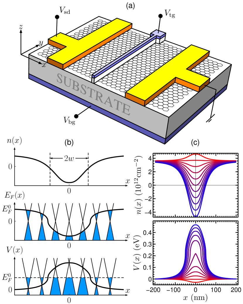
A theoretical study of transport in graphene, whether based on Dirac theory or the TBM formalism, requires the potential as an input, which actually means the local energy offset of the Dirac point and is often regarded directly as the electric potential. In fact, the application of a gate voltage does not directly raise the Dirac cone by ( being the electron charge) but enhances or depletes the carrier density, hence raising or lowering the local Fermi level. For double-gated graphene [Fig. 1(a)], the combination of a top-gate voltage and a back-gate voltage results in a carrier density profile such as that shown in the upper panel in Fig. 1(b). Its energy dependence, , is obtained by integrating the density of states over energy. Defining the local Fermi level as
| (2) |
one obtains the spatially varying height of the filled states, as depicted in the middle panel in Fig. 1(b). In a transport calculation, the global Fermi level is a fixed quantity. Hence to account for the profiles of and , one shifts the local band offset by applying a local potential
| (3) |
as depicted in the lower panel in Fig. 1(b). This completes the extraction of the potential profile from the carrier density profile. Note that the above model makes use of the linear density of states that is normally valid in the experimental range of the carrier density, although the energy dispersion based on the TBM covers the full range. The energy range beyond the Dirac model with a nonlinear density of states can, in principle, be treated within the TBM similarly to the process introduced above, but this would be relevant only far from the energy range of interest.
A realistic carrier density profile depends on the experimental geometry and dielectric material of the gate fabrication. In the experiment in Ref. Young and Kim, 2009, was obtained from an electrostatic simulation and empirically described by
| (4) |
where accounts for the effectiveness of the top-gate relative to the back-gate, is the classical (electron number) capacitance of a -thick SiO2 substrate, and the effective half width of the top-gate is .Young and Kim (2009) Figure 1(c) shows various carrier density profiles described by Eq. (4), subject to and various , and the extracted potential profiles, Eqs. (2) and (3).
II.2 Bulk graphene scattering region
In band theory, the electronic structure of a crystal lattice can be solved by applying the Bloch theorem, which allows us to reduce the problem with infinitely repeated unit cells to only one due to translation invariance along each space dimension. For transport calculations, however, the scattering region of interest is composed of a certain finite-size area and is generally not translationally invariant. For a large flake of double-gated graphene, such as that sketched in Fig. 1(a), the transverse dimension (along ) is typically a few microns in width so that the edges are of minor importance, and we can then assume translational invariance in the direction.
Consider bulk graphene oriented with zigzag carbon chains along the direction. Up to nearest neighbor hopping, the minimal unit cell can be chosen as one hexagon row, i.e., a graphene nanoribbon with zigzag chain number with transverse periodicity , being the bond length. The wave function at the bottom site of the unit cell is related to that at the top site through the Bloch theorem asWimmer (2008) , implying , where is the Bloch momentum defined within . This means that a kinetic hopping across the upper boundary of the unit cell can be equivalently expressed as a periodic hopping modulated by the phase arising from the Bloch theorem. Similarly, one can obtain for the lower boundary . Incorporating these periodic hopping terms, the TBM Hamiltonian for a bulk graphene scattering region can therefore be written as
| (5) |
where () creates (annihilates) a charge carrier at the top (bottom) edge site of the th hexagon along , and , given in Eq. (1), describes an graphene nanoribbon. Note that the above description for a bulk scattering region is restricted neither to nearest neighbor hopping () nor to the material graphene. For the present bulk transport simulation, however, next-nearest-neighbor hopping does not play an important role and we adopt and throughout Sec. III.
II.3 Quantum transport formalism
The quantum transport simulation in the present work is restricted to the linear response regime at zero temperature. Thus the Landauer conductance
| (6) |
is the main object and is obtained by integrating the transmission function
| (7) |
which is equivalent to the Fisher-Lee relation.Fisher and Lee (1981) The Fermi wave vector in Eq. (6) is approximated from the low-energy linear dispersion by . Note that the spin degeneracy is neglected here, while the valley degeneracy is inherently incorporated in .
The retarded Green’s function of the scattering region at energy in Eq. (7) is obtained from
| (8) |
where has been given in Eq. (5) and () is the self-energy due to the left (right) lead composed of a semi-infinite repetition of unit cells. Adopting a Schur-decomposition-based algorithm for the singular hopping matrix type,Wimmer (2008) the periodic hoppings as used in can also be included in and , enabling us to study pure bulk-to-bulk transmission. The spectral matrix functions , with , in Eq. (7) are given by .
III Klein backscattering experiment revisited
III.1 Gate-voltage dependence
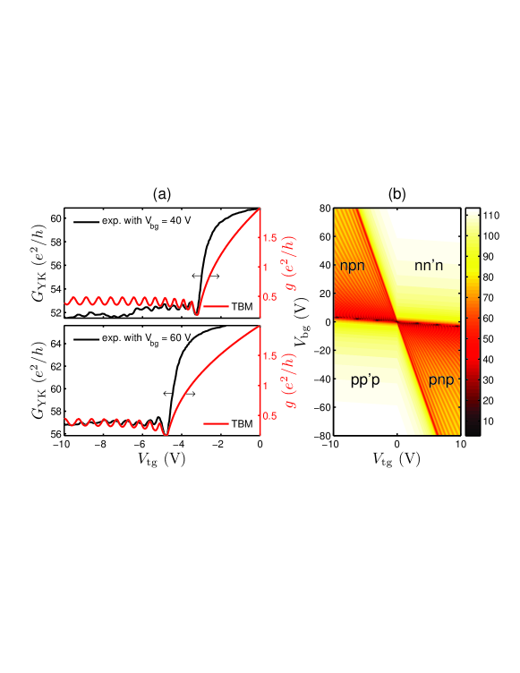
Now we revisit the experiment in Ref. Young and Kim, 2009 by considering the extracted realistic potential and applying the bulk TBM transport formalism introduced above. As shown in Fig. 1(c), the potential profile saturates at roughly , so we consider a scattering region described by with length . The transport is solely supported by the states at the global Fermi level, which is set to . We first investigate the top-gate voltage dependence of the single-mode conductance . In Fig. 2(a), we directly compare the oscillating features of our computed with the experimental data ,111The experimental data compared in this work were extracted from the electronic file of Ref. Young and Kim, 2009, instead of the original data. choosing the measured and curves as explicit examples. In both cases, the general features of the measured oscillating conductance are well captured by our TBM calculation. The Dirac point position of the locally-gated region corresponds to the conductance dip. To the left of this minimum the transport is in the npn regime exhibiting Fabry-Pérot-type oscillations due to interference of backscattered waves between the np and the pn interfaces. To the right of the dip, the transport enters the nn’n regime, where graphene becomes much more transparent than for npn, resulting in the suppression of the interference and the rise in the conductance. This conductance asymmetryHuard et al. (2007); Stander et al. (2009); Cayssol et al. (2009); Low et al. (2009) is the first indirect feature of Klein tunneling, which results in the decay of the transmission with the incident angle in the np regimeCheianov and Fal’ko (2006) and hence a lower integrated conductance, although the tunneling at normal incidence is perfect.
The single-mode spin-degenerate conductance from Eq. (6) has a maximum of and does not reflect the main effect of the back-gate voltage that tunes the global Fermi level : the modulation of the number of modes participating in transport. For bulk graphene at low energy, can be approximated by with , where is the width of the graphene flake. This gives . While the calculation considers the bulk transport across the locally gated region in graphene, the contact resistance between the electrodes and graphene is not included. To compare with the full map of the measured , we temporarily adopt a simple model to account for multiple modes and contact resistance: Assuming an effective width and a low contact resistance , we display the calculated top- and back-gate dependencies of in Fig. 2(b), which qualitatively agrees with Ref. Young and Kim, 2009. Note that the quadrants of are determined by the dependence of the potential profile on and , and do not significantly change with the temporarily introduced parameters and , on which we place less stress in the present work.
III.2 Low-field magnetotransport
Finally, we come to a closer analysis of the low-field magnetotransport. For an incoherent graphene pnp junction a perpendicular magnetic field leads to the increase in the magnetoresistance due to the bending of the electron trajectories.Cheianov and Fal’ko (2006) When the top-gate is narrow enough, such as that in Ref. Young and Kim, 2009, with a width of about , a coherent graphene pnp junction can be formed. Shytov et al.Shytov et al. (2008) proposed a clever way to experimentally test the existence of Klein tunneling, making use of the sign change of the Klein backscattering phase at a weak magnetic field, which in turn results in a half-period shift of the Fabry-Pérot oscillations. Based on this semiclassical treatment the low-field magnetotransport experiment in Ref. Young and Kim, 2009 was regarded as providing evidence of Klein tunneling. In the following we show that our tuning-parameter-free TBM calculation confirms the semiclassical picture and, again, agrees well with the measurement.
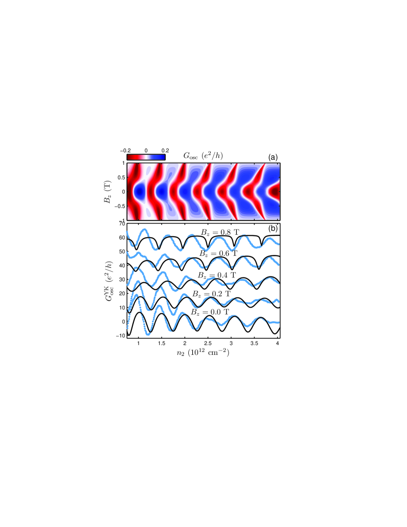
The orbital contribution of the external magnetic field perpendicular to the graphene plane is incorporated in the TBM calculation through the Peierls substitution,Peierls (1933) while the Zeeman term is neglected since the Zeeman splitting is rather small compared to .Das Sarma et al. (2011) To maintain the transverse () translation invariance throughout the whole system while also keeping the longitudinal () translation invariance in the leads, we consider the Landau gauge of only in the scattering region. Inside the left and right leads, however, constant gauge field strengths and must be considered, respectively, where and are the position coordinates of the left-most and right-most atomic site of the scattering region, in order to avoid a discontinuity of the vector potential.
Since the expected phase shift stems from Klein backscattering between the two interfaces inside the locally gated region, the potential tail does not play a crucial role and we reduce the scattering region length to . Following the definition of the oscillating part of the conductance given in Ref. Young and Kim, 2009, we process our data on the single-mode conductance by first computing the odd part of the conductance, , and then subtracting its mean value to obtain . Here [see Eq. (4)] is the carrier density of the locally-gated region. The obtained oscillation fringes of are shown in Fig. 3(a), which is, again, qualitatively consistent with Ref. Young and Kim, 2009. The sudden phase shift, which indicates the presence of perfect transmission and corresponds to the half-period shift predicted by Shytov et al.,Shytov et al. (2008) occurs at magnetic field strengths between and and is in excellent agreement with Ref. Young and Kim, 2009. In Fig. 3(b), the computed is compared with the experimental data Note (1) at various magnetic field strengths (both with offset for clarity).
IV Summary
In conclusion, we have demonstrated the applicability of TBM-based quantum transport simulations for transport in bulk graphene heterojunctions. Applying the Bloch theorem along the transverse dimension, the computational effort for TBM transport through a bulk scattering region is significantly reduced. Together with the realistic potential profile extracted from the carrier density profile of a graphene pnp junction, this method provides a confirmation of the experiment in Ref. Young and Kim, 2009 and its semiclassical theoretical interpretation, at a low computational cost without using free tuning parameters. The quantum transport approach presented here for studying bulk properties is suitable not only for graphene but also for other materials where the TBM works well.
Acknowledgements.
We appreciate valuable discussions with A. Cresti and V. Krueckl. Financial support from the Alexander von Humboldt Foundation (M.-H.L.) and Deutsche Forschungsgemeinschaft within GRK1570 (K.R.) is gratefully acknowledged.References
- Castro Neto et al. (2009) A. H. Castro Neto, F. Guinea, N. M. R. Peres, K. S. Novoselov, and A. K. Geim, Rev. Mod. Phys. 81, 109 (2009).
- Das Sarma et al. (2011) S. Das Sarma, S. Adam, E. H. Hwang, and E. Rossi, Rev. Mod. Phys. 83, 407 (2011).
- Novoselov et al. (2004) K. S. Novoselov, A. K. Geim, S. V. Morozov, D. Jiang, Y. Zhang, S. V. Dubonos, I. V. Grigorieva, and A. A. Firsov, Science 306, 666 (2004).
- Cheianov and Fal’ko (2006) V. V. Cheianov and V. I. Fal’ko, Phys. Rev. B 74, 041403 (2006).
- Katsnelson et al. (2006) M. I. Katsnelson, K. S. Novoselov, and A. K. Geim, Nat. Phys. 2, 620 (2006).
- Klein (1929) O. Klein, Zeitschrift für Physik 53, 157 (1929).
- Beenakker (2008) C. W. J. Beenakker, Rev. Mod. Phys. 80, 1337 (2008).
- Allain and Fuchs (2011) P. Allain and J. Fuchs, Eur. Phys. J. B 83, 301 (2011).
- Huard et al. (2007) B. Huard, J. A. Sulpizio, N. Stander, K. Todd, B. Yang, and D. Goldhaber-Gordon, Phys. Rev. Lett. 98, 236803 (2007).
- Williams et al. (2007) J. R. Williams, L. DiCarlo, and C. M. Marcus, Science 317, 638 (2007).
- Özyilmaz et al. (2007) B. Özyilmaz, P. Jarillo-Herrero, D. Efetov, D. A. Abanin, L. S. Levitov, and P. Kim, Phys. Rev. Lett. 99, 166804 (2007).
- Liu et al. (2008) G. Liu, J. J. Velasco, W. Bao, and C. N. Lau, Appl. Phys. Lett. 92, 203103 (2008).
- Gorbachev et al. (2008) R. V. Gorbachev, A. S. Mayorov, A. K. Savchenko, D. W. Horsell, and F. Guinea, Nano Letters 8, 1995 (2008), pMID: 18543979, http://pubs.acs.org/doi/pdf/10.1021/nl801059v .
- Stander et al. (2009) N. Stander, B. Huard, and D. Goldhaber-Gordon, Phys. Rev. Lett. 102, 026807 (2009).
- Young and Kim (2009) A. F. Young and P. Kim, Nat. Phys. 5, 222 (2009).
- Nam et al. (2011) S.-G. Nam, D.-K. Ki, J. W. Park, Y. Kim, J. S. Kim, and H.-J. Lee, Nanotechnology 22, 415203 (2011).
- Zhang and Fogler (2008) L. M. Zhang and M. M. Fogler, Phys. Rev. Lett. 100, 116804 (2008).
- Shytov et al. (2008) A. V. Shytov, M. S. Rudner, and L. S. Levitov, Phys. Rev. Lett. 101, 156804 (2008).
- Low et al. (2009) T. Low, S. Hong, J. Appenzeller, S. Datta, and M. S. Lundstrom, IEEE Trans. Electron Devices 56, 1292 (2009).
- Yamakage et al. (2009) A. Yamakage, K. I. Imura, J. Cayssol, and Y. Kuramoto, EPL 87 (2009).
- Low and Appenzeller (2009) T. Low and J. Appenzeller, Phys. Rev. B 80, 155406 (2009).
- Rossi et al. (2010) E. Rossi, J. H. Bardarson, P. W. Brouwer, and S. Das Sarma, Phys. Rev. B 81, 121408 (2010).
- Ramezani Masir et al. (2010) M. Ramezani Masir, P. Vasilopoulos, and F. M. Peeters, Phys. Rev. B 82, 115417 (2010).
- Liu et al. (2012) M.-H. Liu, J. Bundesmann, and K. Richter, Phys. Rev. B 85, 085406 (2012).
- Grosso and Parravicini (2000) G. Grosso and G. P. Parravicini, Solid State Physics (Academic Press, New York, 2000).
- Datta (1995) S. Datta, Electronic Transport in Mesoscopic Systems (Cambridge University Press, Cambridge, 1995).
- Note (1) The experimental data compared in this work were extracted from the electronic file of Ref. \rev@citealpnumYoung2009, instead of the original data.
- Wimmer (2008) M. Wimmer, Quantum transport in nanostructures: From computational concepts to spintronics in graphene and magnetic tunnel junctions, Ph.D. thesis, Universität Regensburg (2008).
- Fisher and Lee (1981) D. S. Fisher and P. A. Lee, Phys. Rev. B 23, 6851 (1981).
- Cayssol et al. (2009) J. Cayssol, B. Huard, and D. Goldhaber-Gordon, Phys. Rev. B 79, 075428 (2009).
- Peierls (1933) R. Peierls, Zeitschrift für Physik A Hadrons and Nuclei 80, 763 (1933).