Emergent quantum confinement at topological insulator surfaces
Bismuth-chalchogenides are model examples of three-dimensional topological insulators. Hasan:Rev.Mod.Phys.:82(2010)3045--3067 Their ideal bulk-truncated surface hosts a single spin-helical surface state, Zhang:NaturePhys.:5(2009)438--442; Xia:NaturePhys.:5(2009)398--402 which is the simplest possible surface electronic structure allowed by their non-trivial topology. Kane:Phys.Rev.Lett.:95(2005)146802 They are therefore widely regarded ideal templates to realize the predicted exotic phenomena and applications of this topological surface state. However, real surfaces of such compounds, even if kept in ultra-high vacuum, rapidly develop a much more complex electronic structure Bianchi:NatureCommun.:1(2010)128; King:Phys.Rev.Lett.:107(2011)096802 whose origin and properties have proved controversial. Hsieh:Nature:460(2009)1101--1105; Bianchi:NatureCommun.:1(2010)128; King:Phys.Rev.Lett.:107(2011)096802; Bianchi:Phys.Rev.Lett.:107(2011)086802; Benia:Phys.Rev.Lett.:107(2011)177602; Wray:NaturePhys.:7(2011)32--37; Zhu:Phys.Rev.Lett.:107(2011)186405; Eremeev:arXiv:1107:3208:(2011); Menshchikova:JETPLetters:94(2011)106-111; Wray:arXiv:1105.4794:(2011); Ye:arXiv:1112.5869:(2011); Valla:Phys.Rev.Lett.:108(2012)117601; Vergniory:JETPLett.:95(2012)230--235; Chen:Proc.Nat.Acad.Sci.:109(2012)3694 Here, we demonstrate that a conceptually simple model, implementing a semiconductor-like band bending in a parameter-free tight-binding supercell calculation, can quantitatively explain the entire measured hierarchy of electronic states. In combination with circular dichroism in angle-resolved photoemission (ARPES) experiments, we further uncover a rich three-dimensional spin texture of this surface electronic system, resulting from the non-trivial topology of the bulk band structure. Moreover, our study reveals how the full surface-bulk connectivity in topological insulators is modified by quantum confinement.
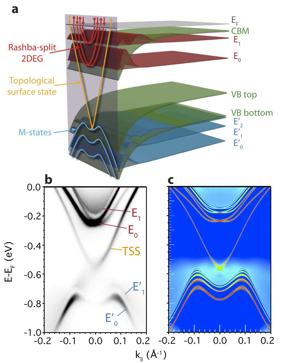
Topological insulators (TIs) are an exotic state of quantum matter, guaranteed to have metallic edge or surface states due to an inverted ordering of their bulk electronic bands. The corresponding topological invariants dictate that there must be an odd number of such states intersecting the Fermi level between each pair of surface time-reversal invariant momenta (TRIM). In the most widely investigated bismuth-chalchogenide family of TIs, there is just one of these so-called topological surface states (TSSs) creating a single Dirac cone around the Brillouin zone centre. Zhang:NaturePhys.:5(2009)438--442; Xia:NaturePhys.:5(2009)398--402; Chen:Science:325(2009)178--181; Bianchi:NatureCommun.:1(2010)128; Scanlon:AdvMat However, exposure to even the minute amount of residual gas in an ultra-high vacuum chamber induces a drastic reconstruction of the surface electronic structure (Fig. 1). The Dirac point shifts to higher binding energies, indicating more electron-rich surfaces. Hsieh:Nature:460(2009)1101--1105; Bianchi:NatureCommun.:1(2010)128; King:Phys.Rev.Lett.:107(2011)096802 More importantly, additional pairs of two-dimensional, almost parabolic states emerge in the vicinity of the bulk conduction band, Bianchi:NatureCommun.:1(2010)128 which develop large Rashba-type splittings, King:Phys.Rev.Lett.:107(2011)096802 while new ladders of M-shaped states are created in the original bulk valence bands. Bianchi:NatureCommun.:1(2010)128; Bianchi:Phys.Rev.Lett.:107(2011)086802 Given their propensity for formation, these must be considered part of the intrinsic electronic structure of the surface of any realistic TI, for example when exposed to air or interfaced to another material. However, their existence is not predicted by idealized theoretical models of the bulk-truncated surface, Zhang:NaturePhys.:5(2009)438--442 and has proved controversial. Recent proposals attribute their formation to a variety of electronic or structural modifications of the crystal host, Hsieh:Nature:460(2009)1101--1105; Bianchi:NatureCommun.:1(2010)128; King:Phys.Rev.Lett.:107(2011)096802; Bianchi:Phys.Rev.Lett.:107(2011)086802; Benia:Phys.Rev.Lett.:107(2011)177602; Wray:NaturePhys.:7(2011)32--37; Zhu:Phys.Rev.Lett.:107(2011)186405; Eremeev:arXiv:1107:3208:(2011); Menshchikova:JETPLetters:94(2011)106-111; Wray:arXiv:1105.4794:(2011); Ye:arXiv:1112.5869:(2011); Valla:Phys.Rev.Lett.:108(2012)117601; Vergniory:JETPLett.:95(2012)230--235; Chen:Proc.Nat.Acad.Sci.:109(2012)3694 but to date no single model has been able to simultaneously reproduce the number and binding energies of the experimentally-observed electronic states as well as the magnitude of their measured Rashba-type splittings.
In the following, we show that this can be achieved taking account of only a single electronic phenomenon – a near-surface electrostatic potential variation. Such intrinsic electric fields are familiar from surface space-charge regions in conventional semiconductors, King:Phys.Rev.Lett.:101(2008)116808; Monch:Semiconductorsurfacesandinterfaces(2001) and are also formed at interfaces where they can be modulated using applied gate voltages. Thus, our findings are not only relevant to understand the free surfaces of topological insulators, but also their use in transistor-style or other thin-film device architectures, which may ultimately provide a route towards room temperature spintronics. Here, we consider Bi2Se3 as a model example, but our computational approach can be freely adapted to virtually all TIs, such as other emerging Bi-chalcogenides or the half-Heusler alloys, Lin:NatureMater.:9(2010)546--549 where we would expect a similarly striking role of band bending at free surfaces, interfaces, or in devices.
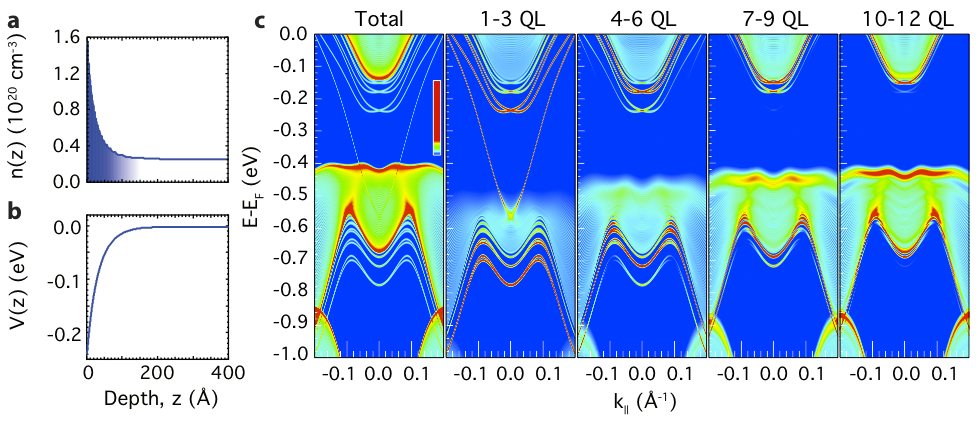
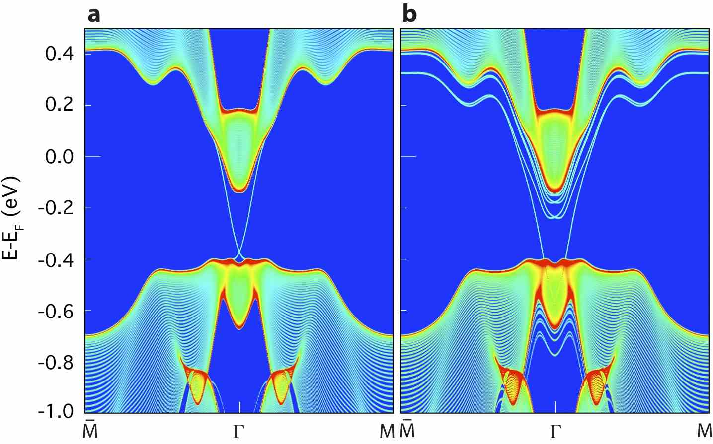
We implement such a band bending scenario within a 120 quintuple-layer (QL) tight-binding supercell calculation (see Methods). Without incorporating any band bending, our supercell model yields a single TSS spanning from the bulk valence to conduction bands (Supplementary Fig. S1), in good agreement with both first-principles slab calculations Zhang:NaturePhys.:5(2009)438--442 and our experimental measurements of the pristine surface (Supplementary Fig. S2). Additionally including an electrostatic potential variation, we find a hierarchy of electronic states that is in excellent agreement with our experimental angle-resolved photoemission (ARPES) measurements of a doped TI surface (Fig. 1(b,c)). fnote1 This agreement is remarkable, given that we do not adjust any parameters in our calculation. All tight-binding matrix elements are obtained from an ab-initio calculation of the bulk electronic structure. The magnitude of the potential change is fixed by the experimentally-measured shift of the Dirac point between a pristine cleaved surface and the -type doped one (see Supplementary Fig. S2), and its functional form follows from a solution of Poisson’s equation. King:Phys.Rev.B:77(2008)125305 We stress that our approach does not require any additional modifications beyond an electrostatic potential, such as a huge increased van der Waals gap size Eremeev:arXiv:1107:3208:(2011); Menshchikova:JETPLetters:94(2011)106-111; Ye:arXiv:1112.5869:(2011); Vergniory:JETPLett.:95(2012)230--235, other artificial detachments of a finite number of crystal layers Zhu:Phys.Rev.Lett.:107(2011)186405, or the formation of new topological surface states Wray:NaturePhys.:7(2011)32--37.
Rather, all of the new electronic states observed experimentally arise simply due to the perturbative effect of the electrostatic potential in the system, which causes a triangular-like downward bending of the bulk electronic bands close to the surface by almost 250 meV (Fig. 2(b)). Combined with the large potential step at the material/vacuum interface, this creates a near-surface quantum well for electrons. The bulk conduction band states are consequently restructured into ladders of multiple subband states. King:Phys.Rev.Lett.:104(2010)256803; Bianchi:NatureCommun.:1(2010)128; Meevasana:NatureMater.:10(2011)114--118 Our layer-resolved calculations (Fig. 2) show that the lowest such subband, lying deep within the potential well, is localized in the topmost few quintuple layers (QL) of the structure: The electrons that populate this subband are free to move parallel to the surface, but are strongly confined perpendicular to it, forming a two-dimensional electron gas (2DEG). This state exhibits a strong Rashba spin-orbit splitting, whose calculated magnitude reproduces our experimental observations. Higher-lying states of the subband ladder are less strongly bound within the surface quantum well and contribute significant weight as far as 10–15 QL below the sample surface. The smaller spin splitting observed experimentally for these higher-lying states is again reproduced by our model calculations, confirming that the Rashba splitting is driven by the potential gradient of the confining electrostatic potential. King:Phys.Rev.Lett.:107(2011)096802 Similar to the conduction band 2DEG, a ladder of subbands is also observed in the valence band near the zone center. These hole-like states become quantum confined between the surface and the upper edge of a projected bulk band gap Zhang:NaturePhys.:5(2009)438--442; Bianchi:Phys.Rev.Lett.:107(2011)086802, as shown schematically in Fig. 1(a). We also find a small spin splitting of these states, which is not resolved experimentally. Its location, around the top of their M-shaped dispersions, indicates a subtle interplay of spin-orbit interactions between the valence and conduction band subbands. M.S.Bahramy:PRB84(2011)041202R Thus, despite its conceptual simplicity, the band bending has dramatic consequences for the surface electronic structure. Driven by an emergent role of quantum size effects, it leads to a hierarchy of electronic states in both energy and spatial extent, spanning from the two-dimensional limit of the TSS and lowest quantum well states of the conduction and valence bands to the three-dimensional continuum.
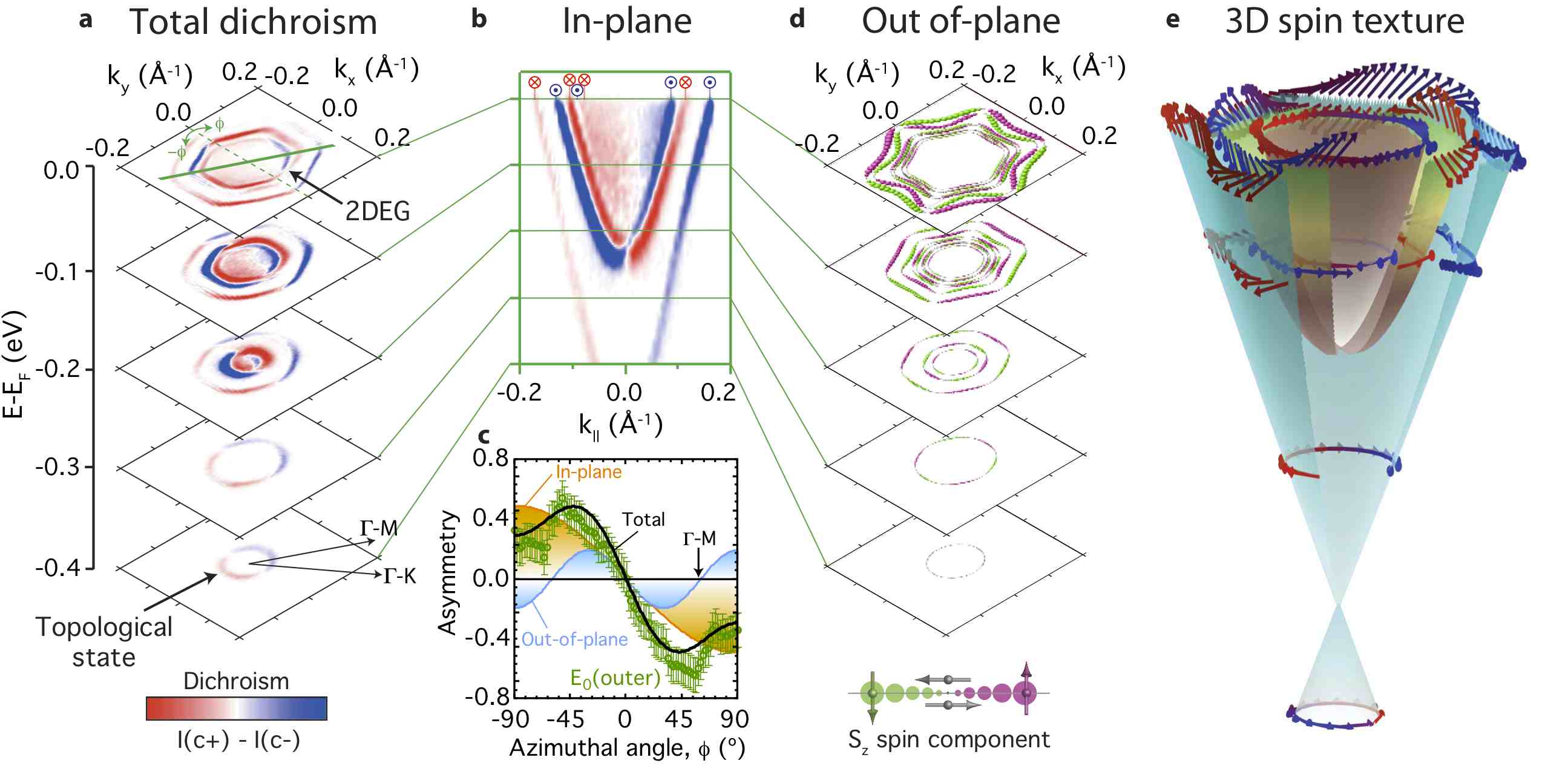
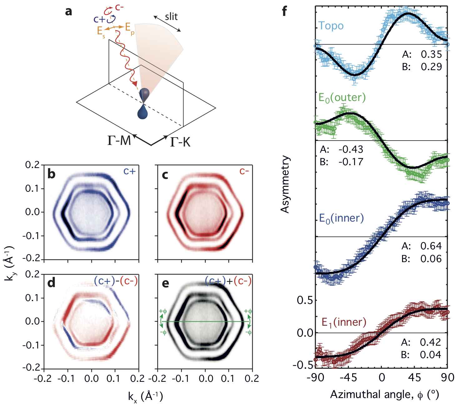
Intriguingly, we find an anti-correlation between this electronic dimensionality, and that of the states’ spin texture. This is revealed experimentally via an asymmetry in the matrix element for photoemission when the system is excited by right and left circularly polarized light, respectively. Such circular dichroism has previously been suggested to directly Wang:Phys.Rev.Lett.:107(2011)207602 or indirectly Park:Phys.Rev.Lett.:108(2012)046805 probe the spin of the isolated TSS. Wang:Phys.Rev.Lett.:107(2011)207602; Park:Phys.Rev.Lett.:108(2012)046805; Ishida:Phys.Rev.Lett.:107(2011)077601 Here, we adopt this concept to show that the full three-dimensional spin texture of the entire low-energy surface electronic structure can be extracted in a similar way. Along the - mirror direction, symmetry requires that the spin must lie entirely within the surface plane. Fu:Phys.Rev.Lett.:103(2009)266801 Our measurements of CD extracted along this direction (Fig. 3(b)) are therefore representative of the in-plane spin texture, and indicate an alternating left-right-left-right-left helicity for consecutive Fermi surface sheets of the TSS and first (E0) and second (E1) quantized conduction subbands. Away from this direction, dichroism of the inner E0 and both E1 2DEG Fermi surface sheets vary sinusoidally with angle, , around the Fermi surface (shown in Supplementary Information). This reveals a model Rashba-like Bychkov:JETPLett.:39(1984)78 helical spin texture of these states, with the spin polarised entirely in the surface plane at all energies. However, for the more spatially-localized TSS and outermost 2DEG states, the dichroism additionally develops a strong ) component which is maximal along - and zero along - (Fig. 3(c) and Supplementary Information). This reflects a strong out-of-plane spin polarization close to the Fermi level, which is correlated with hexagonal warping of the electronic states, Fu:Phys.Rev.Lett.:103(2009)266801 and again switches sign between neighbouring states. Thus, not only does the band bending promote the creation of additional Fermi surface sheets, it also leads to complex band- and binding-energy dependent three-dimensional spin-textures of the resulting electronic system, as summarized in Fig. 3(e). Together, this will cause significant complications for the interpretation of spin-dependent transport experiments, and inter-band processes will weaken the topological protection against backscattering commonly assumed for the TSS of these compounds. Nonetheless, we note that our resolution limited linewidths of Å-1 () indicate that the intrinsic scattering remains relatively weak for all Fermi surface sheets.
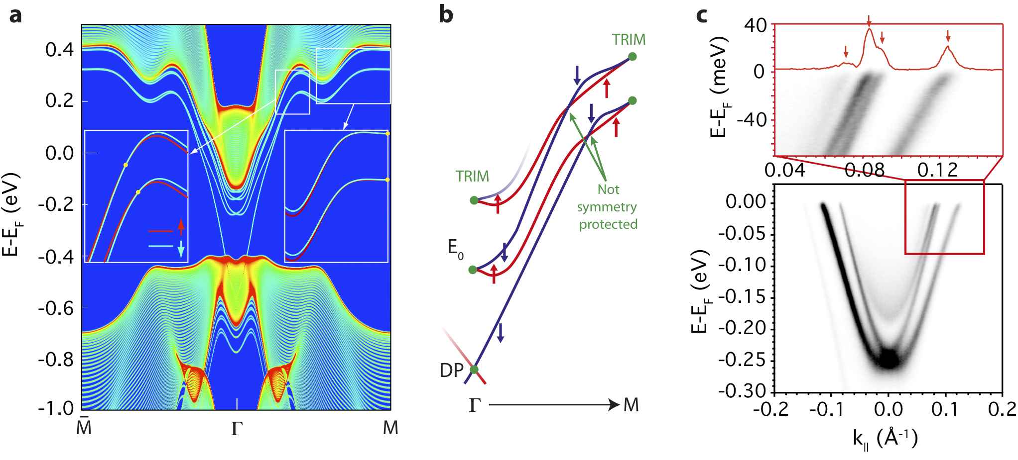
The non-trivial spin texture of these states also raises questions over their interplay. For any system with TR symmetry, the electronic states must be spin-degenerate at TRIM, even though a breaking of inversion symmetry by the confining potential and surface allows a lifting of the spin degeneracy at arbitrary -points. The hexagonal surface Brillouin zone of topological insulators such as Bi2Se3 contains TRIM -points at the zone-centre ( point) and at the side-centre () point. Fig. 4(a) shows the electronic structure calculated along the entire - direction. At the point, each Rashba-split pair of 2DEG states clearly become degenerate. For the TSS, this initially appears to be complicated by the presence of bulk states, with the Dirac point looking to be buried deep in the bulk valence band. However, locally, the TSS is still situated within a projected band gap of the (bent) bulk bands, and so remains a well defined surface state (unlike the 2DEG states which are located within, and indeed derived from, the projected bulk-like bands). Indeed, our layer-projected calculations (Fig. 2) reveal that the Kramer’s degeneracy of the TSS is preserved in the presence of the band bending potential, contrary to previous suggestions of a band gap opening in the surface spectrum at the Dirac point. Wray:NaturePhys.:7(2011)32--37; Wray:arXiv:1105.4794:(2011)
At the -point, our calculations reveal that the TSS connects to the outer branch of the lower 2DEG state. Assuming a spin-down state for the TSS, the pairing 2DEG state has no other choice but to be spin-up. Its spin-down partner must then become connected with the outer branch of the second subband to satisfy TR symmetry for these states, thereby dictating the overall up-down-up-down-up spin configuration discussed above. Fundamentally, this pair-exchange follow from the non-trivial topology of the bulk band structure. This requires that the TSS must connect from the bulk valence to conduction bands. Now, however, the original bulk bands have become quantized into two-dimensional subband states in the vicinity of the surface, and our calculations reveal that it is to these subbands which the topological state connects. We note that this requires the outer and inner branches of the 2DEG states to diverge from each other at large -vectors, in stark contrast to conventional Rashba systems Ishizaka:Nat.Mater.:10(2011)521 in which the spin-split bands merge again at zone-edge TRIM.
Hexagonal warping of the electronic states can additionally induce accidental degeneracies along high-symmetry lines, Bahramy:Nat.Commun:3(2012)679; Basak:PRB84:(2011)121401(R) as seen in Fig. 4. However, as these are not protected by any fundamental symmetry, introduction of perturbations in the system can shift, or even completely remove, such accidental degeneracies. Experimentally, the inner branch of the lower 2DEG state and outer branch of the upper 2DEG state can be seen to approach each other at low binding energies (Fig. 4(c)), consistent with their proximity to the accidental crossing predicted in our calculations. However, contrary to previous reports Wray:NaturePhys.:7(2011)32--37; Wray:arXiv:1105.4794:(2011), our high-resolution measurements reveal that the occupied bands remain nondegenerate and exhibit rather parallel dispersion close to the Fermi level, which could be indicative of an avoided crossing. Understanding whether interactions not included in our theoretical treatment play a role in avoiding the accidental degeneracies will be crucial to unravel surface-bulk coupling in these materials, and the role of interactions in limiting mobilities of spin-polarized surface transport in topological insulators.
Methods
Theory: Relativistic electronic structure calculations were carried out within the context of density functional theory using the Perdew-Burke-Ernzerhof exchange-correlation functional Perdew:PRL:77(1996)3865 and the augmented plane wave plus atomic orbitals (APW-LO) method as implemented in the WIEN2K program. wien2k For all the atoms, the muffin-tin radius was set to 2.5 Bohr and the maximum modulus of reciprocal vectors was chosen such that . The primitive cell was considered to be hexagonal (space group: ) with lattice parameters and atomic positions taken from experiment. Vicente:InrogChem:38(1999)2131 The corresponding BZ was sampled using a -mesh. To simulate the effect of band bending, a 120 QL tight-binding supercell Hamiltonian was constructed by downfolding the APW-LO Hamiltonian using maximally localized Wannier functions (MLWF’s). souza; mostofi; kunes We chose valence orbitals of Bi and Se as the projection centers of MLWF’s. The bending potential was obtained by solving the coupled Poisson-Schrödinger equation, King:Phys.Rev.B:77(2008)125305 assuming a static dielectric constant of 70. King:Phys.Rev.Lett.:107(2011)096802 The resulting potential was then added to the onsite terms of the tight-binding sucpercell Hamiltonain. The (QL-projected) surface band structure was eventually obtained by diagonalizing the supcercell Hamiltonian (and projecting the resulting eigenstates onto the MLWF’s of respective surface QL’s).
Experiment: Bi2Se3 crystals were prepared by reacting high purity elements (5N) of Bi and Se in sealed, evacuated quartz tubes at 850∘C for 2 days, followed by cooling at 2-3∘C/h to 650∘C. The crystals were annealed at this temperature for 7 days before quenching to room temperature. ARPES measurements were performed at 10 K using circularly-polarized light with photon energies of 20–30 eV and a Scienta R4000 hemispherical analyser at the SIS beamline of the Swiss Light Source. Surface doping was achieved by depositing potassium on freshly-cleaved samples from a properly outgassed SAES K getter source.
Acknowledgements
We are grateful for support from the UK EPSRC, the ERC, and the Japan Society for the Promotion of Science (JSPS) through the ‘Funding Program for World-Leading Innovative R&D on Science and Technology (FIRST Program)’, initiated by the council for Science and Technology Policy (CSTP).
References
- (1) Hasan, M. Z. & Kane, C. L. Colloquium: Topological insulators. Rev. Mod. Phys. 82, 3045–3067 (2010).
- (2) Zhang, H. et al. Topological insulators in Bi2Se3, Bi2Te3 and Sb2Te3 with a single Dirac cone on the surface. Nature Phys. 5, 438–442 (2009).
- (3) Xia, Y. et al. Observation of a large-gap topological-insulator class with a single Dirac cone on the surface. Nature Phys. 5, 398–402 (2009).
- (4) Kane, C. L. & Mele, E. J. topological order and the quantum spin hall effect. Phys. Rev. Lett. 95, 146802 (2005).
- (5) Bianchi, M. et al. Coexistence of the topological state and a two-dimensional electron gas on the surface of Bi2Se3. Nature Commun. 1, 128 (2010).
- (6) King, P. D. C. et al. Large tunable rashba spin splitting of a two-dimensional electron gas in Bi2Se3. Phys. Rev. Lett. 107, 096802 (2011).
- (7) Bianchi, M., Hatch, R. C., Mi, J., Iversen, B. B. & Hofmann, P. Simultaneous quantization of bulk conduction and valence states through adsorption of nonmagnetic impurities on Bi2Se3. Phys. Rev. Lett. 107, 086802 (2011).
- (8) Hsieh, D. et al. A tunable topological insulator in the spin helical Dirac transport regime. Nature 460, 1101–1105 (2009).
- (9) Benia, H. M., Lin, C., Kern, K. & Ast, C. R. Reactive chemical doping of the topological insulator. Phys. Rev. Lett. 107, 177602 (2011).
- (10) Wray, L. A. et al. A topological insulator surface under strong Coulomb, magnetic and disorder perturbations. Nature Phys. 7, 32–37 (2011).
- (11) Zhu, Z.-H. et al. Rashba spin-splitting control at the surface of the topological insulator . Phys. Rev. Lett. 107, 186405 (2011).
- (12) Eremeev, S. V., Menshchikova, T. V., Vergniory, M. G. & Chulkov, E. V. New interpretation of the origin of 2DEG states at the surface of layered topological insulators. arXiv:1107:3208 (2011).
- (13) Menshchikova, T., Eremeev, S. & Chulkov, E. On the origin of two-dimensional electron gas states at the surface of topological insulators. JETP Letters 94, 106–111 (2011).
- (14) Wray, L. A. et al. Electron dynamics in topological insulator based semiconductor-metal interfaces (topological - interface based on Bi2Se3 class). arXiv:1105.4794 (2011).
- (15) Ye, M. et al. Relocation of the topological surface state of Bi2Se3 beneath the surface by Ag intercalation. arXiv:1112.5869 (2011).
- (16) Valla, T., Pan, Z.-H., Gardner, D., Lee, Y. S. & Chu, S. Photoemission spectroscopy of magnetic and nonmagnetic impurities on the surface of the topological insulator. Phys. Rev. Lett. 108, 117601 (2012).
- (17) Vergniory, M. G., Menshchikova, T. V., Eremeev, S. V. & Chulkov, E. V. Ab initio study of 2DEG at the surface of topological insulator Bi2Te3. JETP Lett. 95, 230–235 (2012).
- (18) Chen, C. et al. Robustness of topological order and formation of quantum well states in topological insulators exposed to ambient environment. Proc. Nat. Acad. Sci. 109, 3694 (2012).
- (19) Chen, Y. L. et al. Experimental realization of a three-dimensional topological insulator, Bi2Te3. Science 325, 178–181 (2009).
- (20) Scanlon, D. O. et al. Controlling Bulk Conductivity in Topological Insulators: Key Role of Anti-Site Defects. Adv. Mater. 24, 2154–2158 (2012).
- (21) King, P. D. C. et al. Surface Electron Accumulation and the Charge Neutrality Level in In2O3. Phys. Rev. Lett. 101, 116808 (2008).
- (22) Mönch, W. Semiconductor surfaces and interfaces (Springer, Berlin, 2001).
- (23) Lin, H. et al. Half-Heusler ternary compounds as new multifunctional experimental platforms for topological quantum phenomen. Nature Mater. 9, 546–549 (2010).
- (24) The effective mass is slightly overestimated in our model, which stems from a small overestimation of this quantity in our bulk LDA calculations.
- (25) King, P. D. C., Veal, T. D. & McConville, C. F. Nonparabolic coupled Poisson-Schrödinger solutions for quantized electron accumulation layers: Band bending,charge profile,and subbands at InN surfaces. Phys. Rev. B 77, 125305 (2008).
- (26) King, P. D. C. et al. Surface Band-Gap Narrowing in Quantized Electron Accumulation Layers. Phys. Rev. Lett. 104, 256803 (2010).
- (27) Meevasana, W. et al. Creation and control of a two-dimensional electron liquid at the bare SrTiO3 surface. Nature Mater. 10, 114–118 (2011).
- (28) Bahramy, M. S. and Arita, R. & Nagaosa, N. Origin of giant bulk Rashba splitting: Application to BiTeI. Phys. Rev. B 84, 041202(R) (2011).
- (29) Wang, Y. H. et al. Observation of a warped helical spin texture in from circular dichroism angle-resolved photoemission spectroscopy. Phys. Rev. Lett. 107, 207602 (2011).
- (30) Park, S. R. et al. Chiral orbital-angular momentum in the surface states of . Phys. Rev. Lett. 108, 046805 (2012).
- (31) Ishida, Y. et al. Common origin of the circular-dichroism pattern in angle-resolved photoemission spectroscopy of and . Phys. Rev. Lett. 107, 077601 (2011).
- (32) Bychkov, Y. A. & Rashba, E. I. Properties of a 2D electron gas with lifted spectral degeneracy. JETP Lett. 39, 78 (1984).
- (33) Fu, L. Hexagonal warping effects in the surface states of the topological insulator Bi2Te3. Phys. Rev. Lett. 103, 266801 (2009).
- (34) Ishizaka, K. et al. Giant Rashba-type spin splitting in bulk BiTeI. Nat. Mater. 10, 521–526 (2011).
- (35) Bahramy, M. S. et al. Emergence of non-centrosymmetric topological insulating phase in BiTeI under pressure. Nat. Commun. 3, 679 (2012).
- (36) Basak, S. et al. Spin texture on the warped Dirac-cone surface states in topological insulators. Phys. Rev. B 84, 121401(R) (2011).
- (37) Perdew, J. P., Burke, K. & Ernzerhof, M. Generalized Gradient Approximation Made Simple. Phys. Rev. Lett 77, 3865-3868) (1996).
- (38) Blaha, P. et al., WIEN2K package, Version 10.1 (2010); available at, http://www.wien2k.at.
- (39) Vicente, C. P. et al. X-ray diffraction and 119Sn Mössbauer spectroscopy study of new phase in the Bi2Se3-SnSe system: SnBi4Se7. Inorg. Chem. 38, 2131-2135 (1999).
- (40) Souza, I. et al. Maximally localized Wannier functions for entangled energy bands. Phys. Rev. B 65, 035109 (2001).
- (41) Mostofi, A. A. et al. Wannier90: A tool for obtaining maximally localized Wannier functions. Comp. Phys. Commun. 178, 685 699 (2008).
- (42) Kuneš, J. et al. WIEN2WANNIER: From linearized augmented plane waves to maximally localized Wannier functions. Comp. Phys. Commun. 181, 1888 1895 (2010).
Supplementary Information
SI 1 Electron doping of the surface
The surface projection of our ab-initio-derived tight-binding model for the ideal bulk-truncated surface of Bi2Se3 is shown in Fig. S1(a). Besides the projected bulk bands, the topological surface state gives rise to a clear Dirac-like feature spanning from the bulk valence to conduction bands, in good agreement with previous idealized first-principles models of the surface electronic structure of topological insulators. Zhang:NaturePhys.:5(2009)438--442 A very similar electronic structure is also seen in our experimental measurements of the pristine surface of Bi2Se3, performed immediately after cleaving the sample in ultra-high vacuum. Additionally imposing a near-surface electrostatic potential in our model (i.e., a downward band bending resulting from surface doping) leads to a drastic reconstruction of the electronic structure, as discussed in the main text and shown for comparison in Fig. S1(b).
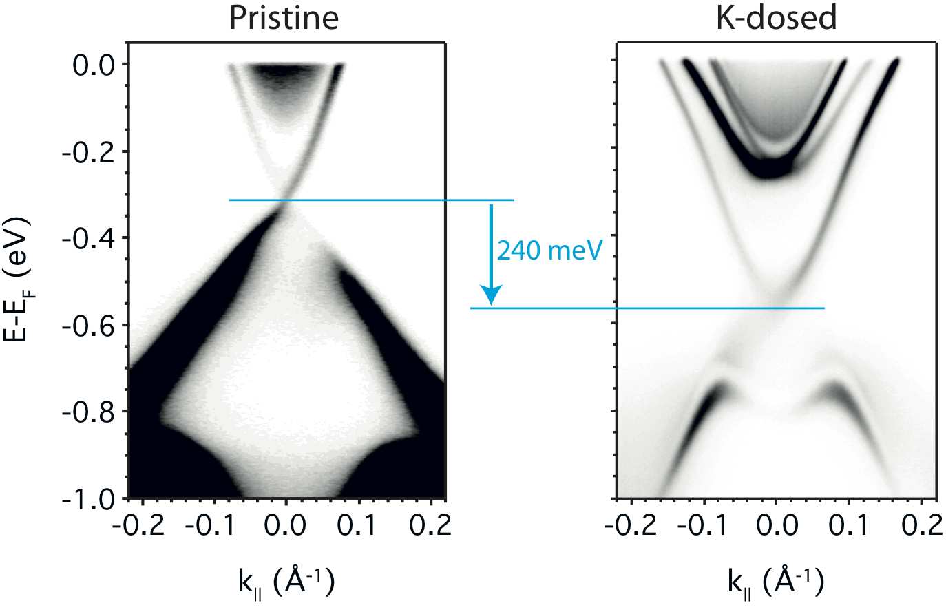
Surface doping via adsorption of residual gas from the vacuum onto the surface of Bi2Se3, and related compounds, is already sufficient to drive time-dependent changes of the electronic structure, which ultimately leads to such surface quantum well formation. Bianchi:NatureCommun.:1(2010)128; King:Phys.Rev.Lett.:107(2011)096802 However, creation of such band bending can be drastically accelerated by deliberately adsorbing minute quantities of a range of molecules or atoms on the surface. King:Phys.Rev.Lett.:107(2011)096802; Bianchi:Phys.Rev.Lett.:107(2011)086802; Benia:Phys.Rev.Lett.:107(2011)177602; Wray:NaturePhys.:7(2011)32--37; Zhu:Phys.Rev.Lett.:107(2011)186405 Here, we employ alkali metal dosing, depositing ML (from XPS analysis) of potassium on the freshly-cleaved sample surface from a properly outgassed SAES K getter source. This causes the spectral changes shown in Fig. S2, including a shift of the Dirac point to higher binding energies by 240 meV, and the emergence of Rashba-split conduction band subbands and M-shaped valence band subbands, as also seen in our theoretical model (Fig. S1(b)) and discussed in detail in the main text.
SI 2 Quantitative analysis of Circular Dichroism
The experimental geometry for the circular dichroism measurements is shown in Fig. S3(a). The analyser entrance slit is oriented along the - direction, and the full electronic structure is measured by tilting the sample around this axis. A clear intensity difference can be observed between the Fermi surface measured in this way using right and left hand circularly polarized light, respectively (Fig. S3(b-d)). Such circular dichroism (CD) has recently been shown to encode the spin-texture of the topological surface state (TSS) in topological insulators (TIs). Wang:Phys.Rev.Lett.:107(2011)207602; Park:Phys.Rev.Lett.:108(2012)046805; Ishida:Phys.Rev.Lett.:107(2011)077601; Jung:Phys.Rev.B:84(2011)245435 We use this method to additionally extract the spin texture of the 2DEG states, as sumarized in the main manuscript. We note that, for the relative changes in CD between the bands that we study here we can neglect final-state effects, as transitions from all of these closely-spaced initial states will go into the same (broad) final state.
To enable quantitative analysis, we define an asymmetry parameter
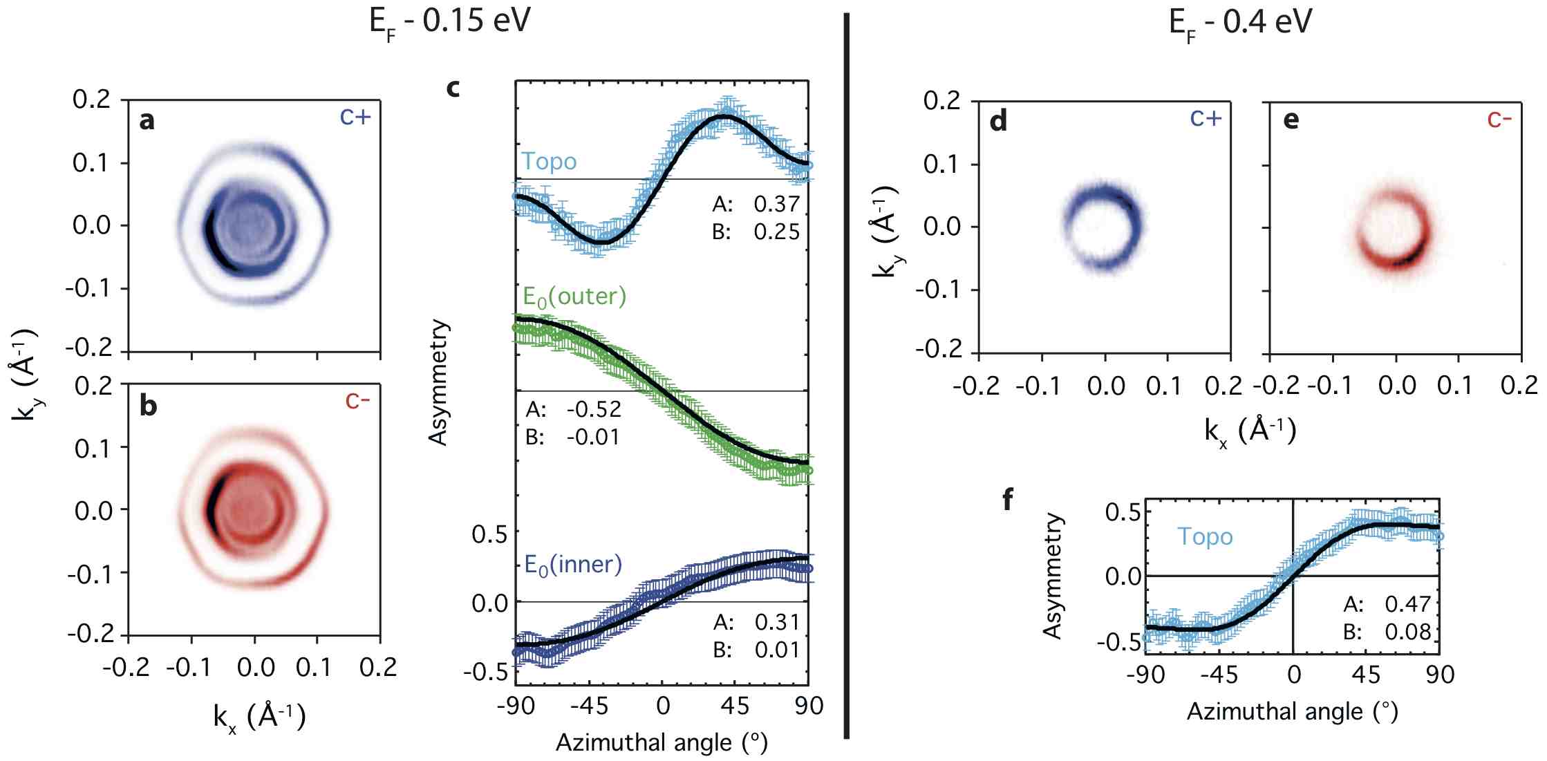
where is the normalized intensity of photoemission measured using right or left circularly polarized light, respectively, at an azimuthal angle around a Fermi surface contour (defined in Fig. S3(e)), with a node in the CD always found for . Such asymmetry measurements are shown at the Fermi level in Fig. S3(f) and at binding energies of 0.15 eV and 0.4 eV in Fig. S4(c) and (f), respectively. These are fit by the function , with the coefficients shown in the figures. CD varying with a simple dependence around the Fermi surface arises from the in-plane winding of the spin around the Fermi surface, while the component results from coupling to the out-of-plane spin component. Wang:Phys.Rev.Lett.:107(2011)207602; Jung:Phys.Rev.B:84(2011)245435; Fu:Phys.Rev.Lett.:103(2009)266801 The ratio of the and components in the fit therefore gives a good measure of the degree of out-of-plane spin polarization. We note that this is the minimal model consistent with the symmetry of the surface Fu:Phys.Rev.Lett.:103(2009)266801. Negligible improvement in the fits was found when including possible higher-order terms (such as a component Jung:Phys.Rev.B:84(2011)245435; Basak:Phys.Rev.B:84(2011)121401), so we neglect these in the following.
The asymmetries around the Fermi surface are shown in Fig. S3(f). The asymmetry changes sign upon moving inwards from the outermost Fermi surface sheet of the topological state to the subsequent Fermi surfaces of the lowest Rashba-split subband () of the 2DEG. This is entirely consistent with the results of spin-resolved photoemission for these states. King:Phys.Rev.Lett.:107(2011)096802 While it is difficult to resolve the outer branch of the second Rashba-split subband (), its spin-split pair is visible as the innermost Fermi surface sheet at positive values in Fig. S3(b–e). The asymmetry of this state has the same sign as the inner branch of the lower subband state (Fig. S3(f)), indicating an overall up-down-up-down-up ordering of the spin for consecutive Fermi surface pockets.
The asymmetry of the inner branch of both the lower and upper ( and ) subbands is well described by a single sinusoid, with negligible component in the fits. The spin therefore lies almost entirely within the surface plane for these near-circular Fermi surfaces, as expected for a simple model Rashba system. Bychkov:JETPLett.:39(1984)78 On the other hand, the asymmetries of the outer branch of the lower () subband and the TSS both contain a substantial component which varies as , indicating a significant canting of the spin out of the surface plane. This is entirely consistent with the strong hexagonal warping of their Fermi surfaces. Fu:Phys.Rev.Lett.:103(2009)266801; Frantzeskakis:Phys.Rev.B:84(2011)155453; Souma:Phys.Rev.Lett.:106(2011)216803; Xu:Science:332(2011)560--564
At energies close to the band bottom of the 2DEG states, such an out-of-plane spin polarization is still present for the TSS (Fig. S4(c)). Now, however, the spin lies within the surface plane not only for the inner but also the outer branch of the lowest 2DEG subband. At higher binding energies still, well below the band bottom of the 2DEG states and approaching the Dirac point, the ideal in-plane helical spin texture is recovered also for the topological state (Fig. S4(f)).
Therefore, not only the direction of the spin winding, but also its effective dimensionality, has a distinct variation with binding energy for each of the multiple electronic bands that make up the complex surface electronic structure of these materials.
References
- (1) Zhang, H. et al. Topological insulators in Bi2Se3, Bi2Te3 and Sb2Te3 with a single Dirac cone on the surface. Nature Phys. 5, 438–442 (2009).
- (2) Bianchi, M. et al. Coexistence of the topological state and a two-dimensional electron gas on the surface of Bi2Se3. Nature Commun. 1, 128 (2010).
- (3) King, P. D. C. et al. Large tunable rashba spin splitting of a two-dimensional electron gas in Bi2Se3. Phys. Rev. Lett. 107, 096802 (2011).
- (4) Bianchi, M., Hatch, R. C., Mi, J., Iversen, B. B. & Hofmann, P. Simultaneous quantization of bulk conduction and valence states through adsorption of nonmagnetic impurities on Bi2Se3. Phys. Rev. Lett. 107, 086802 (2011).
- (5) Benia, H. M., Lin, C., Kern, K. & Ast, C. R. Reactive chemical doping of the topological insulator. Phys. Rev. Lett. 107, 177602 (2011).
- (6) Wray, L. A. et al. A topological insulator surface under strong Coulomb, magnetic and disorder perturbations. Nature Phys. 7, 32–37 (2011).
- (7) Zhu, Z.-H. et al. Rashba spin-splitting control at the surface of the topological insulator . Phys. Rev. Lett. 107, 186405 (2011).
- (8) Wang, Y. H. et al. Observation of a warped helical spin texture in from circular dichroism angle-resolved photoemission spectroscopy. Phys. Rev. Lett. 107, 207602 (2011).
- (9) Park, S. R. et al. Chiral orbital-angular momentum in the surface states of . Phys. Rev. Lett. 108, 046805 (2012).
- (10) Ishida, Y. et al. Common origin of the circular-dichroism pattern in angle-resolved photoemission spectroscopy of and . Phys. Rev. Lett. 107, 077601 (2011).
- (11) Jung, W. et al. Warping effects in the band and angular-momentum structures of the topological insulator Bi2Te3. Phys. Rev. B 84, 245435 (2011).
- (12) Fu, L. Hexagonal warping effects in the surface states of the topological insulator Bi2Te3. Phys. Rev. Lett. 103, 266801 (2009).
- (13) Basak, S. et al. Spin texture on the warped Dirac-cone surface states in topological insulators. Phys. Rev. B 84, 121401(R) (2011).
- (14) Bychkov, Y. A. & Rashba, E. I. Properties of a 2D electron gas with lifted spectral degeneracy. JETP Lett. 39, 78 (1984).
- (15) Frantzeskakis, E. & Grioni, M. Anisotropy effects on rashba and topological insulator spin-polarized surface states: A unified phenomenological description. Phys. Rev. B 84, 155453 (2011).
- (16) Souma, S. et al. Direct measurement of the out-of-plane spin texture in the Dirac-cone surface state of a topological insulator. Phys. Rev. Lett. 106, 216803 (2011).
- (17) Xu, S.-Y. et al. Topological phase transition and texture inversion in a tunable topological insulator. Science 332, 560–564 (2011).