Tunnelling anisotropic magnetoresistance of Fe/GaAs/Ag(001) junctions from first principles: Effect of hybridized interface resonances
Abstract
Results of first-principles calculations of the Fe/GaAs/Ag(001) epitaxial tunnel junctions reveal that hybridization of interface resonances formed at both interfaces can enhance the tunnelling anisotropic magnetoresistance (TAMR) of the systems. This mechanism is manifested by a non-monotonic dependence of the TAMR effect on the thickness of the tunnel barrier, with a maximum for intermediate thicknesses. A detailed scan of -resolved transmissions over the two-dimensional Brillouin zone proves an interplay between a few hybridization-induced hot spots and a contribution to the tunnelling from the vicinity of the point. This interpretation is supported by calculated properties of a simple tight-binding model of the junction which reproduce qualitatively most of the features of the first-principles theory.
pacs:
73.40.Sx, 75.70.Tj, 85.75.Mm,
1 Introduction
Systems and devices with applicability in spintronics include traditional magnetic multilayers and tunnel junctions consisting of several magnetic layers [1, 2, 3] as well as more recent artificial structures containing only a single magnetic part [4, 5]. The former exhibit the well-known giant and tunnelling magnetoresistance effects arising due to changes in the mutual orientation of magnetization directions, the latter are featured especially by properties driven by the spin-orbit (SO) interaction. The so-called tunnelling anisotropic magnetoresistance (TAMR) was observed in systems FM/I/NM, where the FM denotes a ferromagnetic metallic electrode, the NM denotes a non-magnetic metallic electrode, and the I denotes a non-magnetic insulating (semiconducting) barrier [6, 7].
The TAMR effect observed in conventional Fe/GaAs/Au tunnel junctions [7] proved to be rather weak which prevents its direct use. Similarly, a complementary phenomenon, namely, the current (or voltage) induced spin-transfer torques [4], which might be employed for magnetization switching in the FM/I/NM devices, requires a large TAMR effect as a necessary prerequisite for efficient spintronic devices [8]. Recent attempts to enhance the TAMR values included, e.g., modification of the surface structure of the semiconductor layer during the growth process [9] or the use of an antiferromagnetic metal instead of the ferromagnetic one in the magnetic electrode [5]. The latter approach yields strongly enhanced TAMR values, which, however, could be observed only at low temperatures, despite the much higher Néel temperature of the antiferromagnetic material.
The TAMR attracted interest also on theoretical side. A number of various topics were addressed in the framework of phenomenological models. These approaches discussed the role of the anisotropic density of states of the FM electrode [6], the symmetry properties and the interplay of the Rashba and Dresselhaus contributions to the SO interaction, the effect of external magnetic fields and applied bias voltages [7, 10], etc. Ab initio calculations of the TAMR were carried out for tunnel junctions with Fe and Cu electrodes separated by vacuum [11] and GaAs [12] as well as for the Fe/GaAs/Au trilayers [13]. The first-principles studies proved that interface states (resonances) formed at the FM/I interface play an important role in the TAMR phenomenon.
All existing theoretical studies ascribe the TAMR primarily to electronic properties of the FM electrode, the tunnel barrier and their interface, whereas the NM electrode and the I/NM interface are considered to be of secondary importance. In the present paper, we show by means of first-principles calculations for the Fe/GaAs/Ag system and by the study of a simple tight-binding (TB) model Hamiltonian, that the standard picture of the TAMR is not generally valid. In particular, we find that interface resonances at the I/NM interface–when hybridized with those at the FM/I interface–can yield high TAMR values. Moreover, we predict a non-monotonic dependence of the TAMR value on the thickness of the tunnelling barrier and discuss its physical origin.
The paper is organized as follows. The structural model of the Fe/GaAs/Ag junction and the ab initio techniques employed are summarized in section 2 while the obtained results and their discussion are presented in section 3: the properties of the GaAs/Ag interface are presented in section 3.1 and those of the Fe/GaAs/Ag system are contained in section 3.2. The TB model is formulated and studied in section 4 and the summary of the main results is given in the last section.
2 Model and methods
The structural model of the Fe/GaAs/Ag(001) tunnel junction represents a simple generalization of the model for the Fe/GaAs/Cu trilayers [12]. The slab of the zinc-blende (zb) structure of GaAs is attached epitaxially to semiinfinite leads of the body-centered cubic (bcc) Fe and the face-centered cubic (fcc) Ag; the atomic planes are the (001) planes of all three structures. The structure of the Fe/GaAs interface has been assumed without any reconstructions and layer relaxations on the basis of the ideal ratio of the lattice parameters , that is satisfied with a good accuracy for GaAs and Fe. The structure of the GaAs/Ag interface was also assumed without reconstructions; it employed the ideal ratio and the mutual rotation of both bulk structures by around the common (001) axis. The interplanar distance between the adjacent atomic planes of the GaAs and Ag parts was set equal to the arithmetic average of the distances in the bulk GaAs () and the bulk Ag (). The axis of the coordinate system is perpendicular to the atomic planes, while the and axes coincide respectively with the [100] and [010] directions of the fcc lattice, i.e., they point along the directions of the bcc and zb lattices. The GaAs slab contains As-atomic (001) planes with As-termination on both sides; the investigated systems are thus abbreviated as Fe/As(GaAs)n-1/Ag(001).
The electronic structure of the systems was calculated by self-consistent scalar relativistic tight-binding linear muffin-tin orbital (TB-LMTO) method [14, 15, 16]. The calculations were performed using the local spin-density approximation with the Vosko-Wilk-Nusair parametrization of the exchange-correlation potential [17]. The LMTO valence basis , where is the orbital index and is the spin index, was limited to and the so-called empty spheres were used for an efficient treatment of the open zb structure. The low-lying Ga- orbitals were treated as core orbitals so that the valence basis comprised the Ga- orbitals [18]. This choice leads to a good description of the bulk bandstructure of the GaAs concerning both the band gap (around 1.2 eV) and the valence bandwidth (around 6.8 eV), which agree quite well with measured data [19].
The study of the TAMR was based on the conductances evaluated in the current-perpendicular-to-the-planes (CPP) geometry. For this purpose, the scalar relativistic TB-LMTO Hamiltonian was completed by adding an on-site SO term having a simple form, where the atomic-like SO parameters of the atom at the lattice site were calculated from the self-consistent electronic structure [20]. The matrix elements of the SO term have the form
| (1) |
where the symbols and denote respectively the orbital and spin angular momentum operators. The direction of the FM electrode magnetization is given by two angles and , or by the unit vector . These quantities enter the Hamiltonian via the operator in (1), which acts only on the spin indices and which is represented by the spin-1/2 rotation matrix , where the and are two of the Pauli spin matrices [21]. Note that the form of (1) corresponds to the global rotation of the spin quantization axis, whereas the coordinate system for the orbital motion remains unchanged.
The CPP conductances were evaluated in the TB-LMTO Kubo-Landauer formalism [22, 23] as averages of the -dependent transmissions over the two-dimensional (2D) Brillouin zone (BZ). The mixing of both spin channels due to the SO interaction has been implemented similarly to the case of non-collinear layered spin structures [22, 24]. For thicknesses of the GaAs barriers relevant in experiments (), the tunnelling current is carried mainly by the states with -vectors from a small central region of the whole 2D BZ. A sufficiently dense mesh of sampling points (corresponding to -vectors in the full 2D BZ) has been used to get reliable values of the CPP conductances.
3 Results and discussion
3.1 Electronic structure of Ag/GaAs/Ag(001) systems
In recent theoretical studies, the Fe/GaAs(001) system has been attached to a hypothetical bcc(001) Cu electrode since the bulk bcc Cu has a free-electron-like bandstructure and the GaAs/Cu interface has a featureless transmission function [11, 12]. This setup is advantageous for investigations of the role of the Fe/GaAs(001) interface state (resonance) lying in the minority-spin channel at the Fermi energy. This interface resonance gives rise, e.g., to a reversal of spin polarization of the tunnelling current with applied voltage [12] and it can lead to a pronounced TAMR effect [11]. Motivated by these facts, we have focused on electronic properties of the non-magnetic GaAs/Ag(001) interface prior to the study of the Fe/GaAs/Ag junctions.
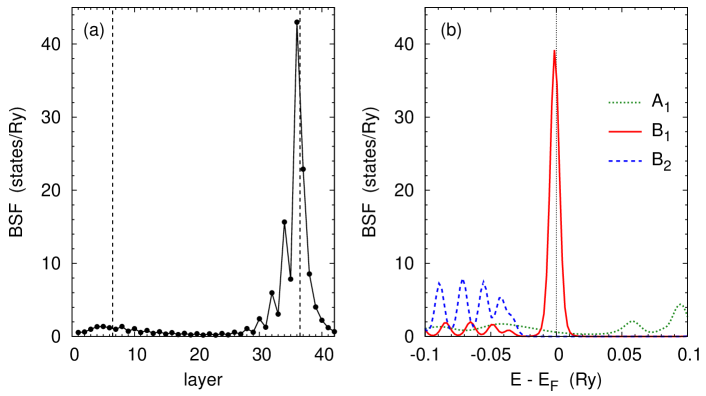
We have thus studied systems Ag/GaAs/Ag(001) with different thicknesses and both terminations (Ga or As) of the GaAs barrier. These studies were done first without the SO interaction. Since the tunnelling current is mostly carried by states with -vectors in the vicinity of the point, we paid special attention to . Figure 1(a) displays the layer-resolved Bloch spectral function of the system Ag/(GaAs)15/Ag(001) for an energy slightly below the Fermi energy ( mRy). One can see a clear indication of an interface state at the GaAs/Ag interface, i.e., at the As-terminated GaAs barrier. The amplitude of the interface state is maximal in the As layer adjacent to the Ag electrode. A similar interface state was found in the Au/GaAs/Au(001) system, located however 10 mRy below the Fermi energy, whereas in the Cu/GaAs/Cu(001) with bcc Cu, no such state appears, in agreement with previous studies [12]. It should be noted that no similar interface state was found at the Ga-terminated boundary of the GaAs barrier in a wide energy interval around the Fermi energy (inside the band gap of GaAs), irrespective of the electrode metal (Cu, Ag, Au).
The origin of the interface state can be understood from the Bloch spectral functions of the boundary As site resolved with respect to the symmetry given by the point group of the interface, namely, the group. This group has four one-dimensional irreducible representations: A1, A2, B1, and B2 [25], of which only the A1 (subspace spanned by orbitals , , and ) is compatible with the symmetry of propagating states of the Ag(001) electrode at the Fermi level. As can be seen in figure 1(b), the interface state is entirely of the symmetry B1 (subspace spanned by orbitals and ), which is incompatible with the propagating states available in the Ag electrode. This incompatibility is an important factor, since the semiinfinite metallic electrode acts essentially like a vacuum half-space in the formation of the interface state.
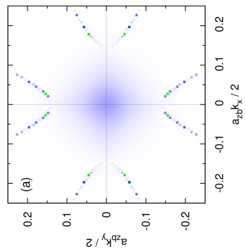
In the Landauer picture of the ballistic transport, interface states do not contribute directly to the system conductance, since the latter is given solely by the transmission coefficients between the propagating channels of the leads [26]. However, if an interface state is coupled, e.g., by a weak interaction to the propagating states, it can become a resonance with a non-negligible effect on the conductance. In the present case, the SO interaction provides such a coupling of the B1-like interface state to the A1-like propagating state, which follows from an analysis of the double group and its irreducible representations: all spin-orbitals belong to the single additional two-dimensional representation of this double group [27]. The influence of the interface resonances on tunnelling is especially strong in symmetric junctions with identical electrodes, where both resonances become hybridized across the tunnel barrier which enhances the conductance appreciably [28]. This phenomenon is illustrated in figure 2, where the -resolved transmissions are compared for the symmetric junction Ag/As(GaAs)14/Ag(001) treated without and with SO coupling. The pronounced enhancement of the in vicinity of the point is clearly visible; the total conductance of the junction increases by one order of magnitude due to the SO interaction. This result indicates importance of the GaAs/Ag interface for the transport behaviour of the Fe/GaAs/Ag system.
3.2 Conductances and TAMR of Fe/GaAs/Ag junctions
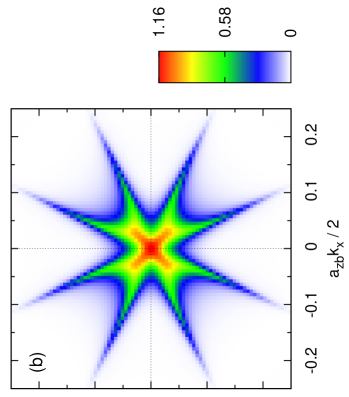
Figure 3 shows the local density of states (DOS) of the central GaAs layer (two neighbouring atomic planes) inside the Fe/As(GaAs)10/Ag(001) junction. The shape of the DOS is bulk-like, with the band gap clearly formed around the Fermi energy and with negligible spin polarization. These features prove that the junction is in a tunnelling regime with metal-induced gap states significantly suppressed for this and higher barrier thicknesses. The tunnelling regime is also manifested by an exponential decay of the conductance with the increasing GaAs thickness , plotted in figure 4(a) for three orientations of the iron magnetic moment, i.e., along the , , and axis. For a given , the conductance is obviously sensitive to the magnetization direction which leads to the TAMR effect. The orientational dependence was studied in detail for magnetization directions in the atomic planes, i.e., as functions of the angle with the fixed value of . The resulting angular dependences, shown in figure 5 for and , reflect the two-fold rotation symmetry (point group ) of the system, in full agreement with previous calculations [13] and measurements [7] performed for similar Fe/GaAs/Au(001) junctions.
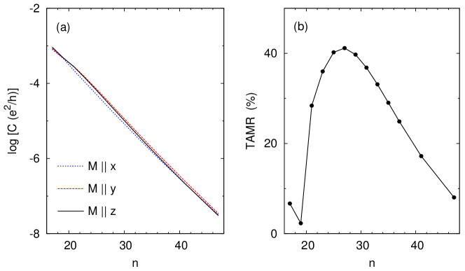

The in-plane TAMR, defined from the angular dependence of the conductance as , is presented in figure 4(b) as a function of the barrier thickness . The calculated TAMR effect is quite large, exceeding 10%, in reasonable agreement with the values calculated for the Fe/GaAs/Au system [13], but about two orders of magnitude stronger than the experimentally observed TAMR values [7]. Moreover, the calculated thickness dependence is non-monotonic with a maximum obtained around corresponding to the GaAs thickness of about 7.5 nm. In order to identify possible reasons for the calculated high TAMR values and the non-monotonic thickness dependence, additional analysis is needed.
-
position TAMR (%) — 41.2 inside Fe 39.4 at Fe/As 3.7 inside GaAs 41.4 at As/Ag 4.7 inside Ag 32.2 at Fe/As and As/Ag 3.6
In general, discrepancy between the calculated and measured transport properties of epitaxial magnetic multilayers can often be ascribed to imperfect atomic structure at the interfaces. The correct treatment of structure defects on an ab initio level employs either supercell techniques [29, 30] or effective medium approaches [23] combined with a particular microscopic model of the structure imperfection. In order to get a rough insight into the sensitivity of the TAMR to the quality of interfaces, we adopted here a simplified approach. We have simulated chemical disorder in the system by a finite imaginary part of the energy arguments of the potential functions in the TB-LMTO Kubo-Landauer formalism [22, 23]. This modification was used only in a few selected atomic planes of the whole system: in two neighbouring planes located at a single interface (Fe/As or As/Ag), at both interfaces, inside the GaAs barrier, or inside the metallic electrodes. The value of mRy was used in all cases. The results for (the thickness corresponding to the maximum TAMR effect in the perfect junctions) are collected in table 1. One can see that the disorder deep inside each part (Fe, GaAs, Ag) of the junction has only a minor influence on the resulting TAMR. However, the interface disorder reduces the TAMR value quite significantly, which proves that at least a part of the difference between the large theoretical values of the TAMR and the much weaker observed effect is due to the interface roughness. Moreover, both interfaces influence the TAMR effect to a similar extent, see table 1, which indicates that they are of equal importance for the calculated trend of the TAMR (figure 4(b)).
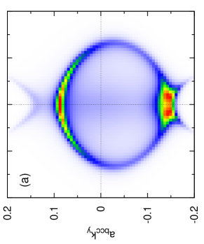
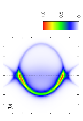
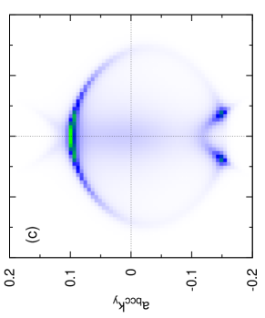
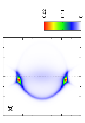
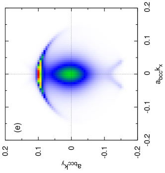
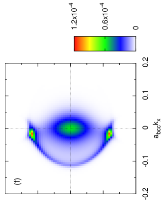
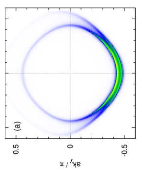
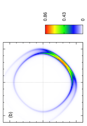
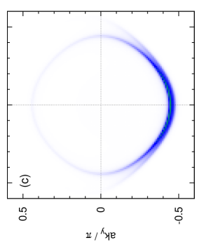
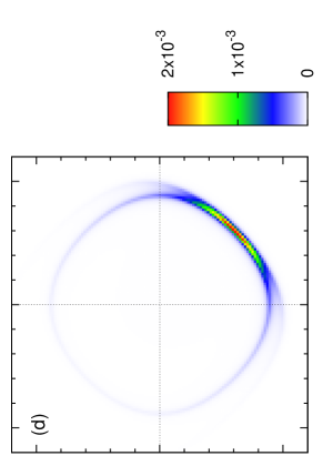
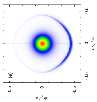
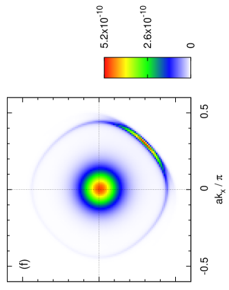
Further insight into the obtained results follows from the -resolved transmissions . Figure 6 shows this quantity for three barrier thicknesses, , , and , and for the magnetization directions along the and axis. Only a small region around the point is included in the figure while the rest of the entire 2D BZ (defined by ) is unimportant for the tunnelling. The maximum TAMR () corresponds to a few hot spots in the plots, see figure 6(c, d); their positions and contributions to the total conductance are strongly sensitive to the direction of the iron magnetic moment. The lower TAMR values for thinner barriers are due to non-negligible contributions of bigger 2D regions to the total conductances, see the case of in figure 6(a, b). On the other hand, the lower TAMR values for very thick barriers () are due to the same hot spots with non-zero -vectors as found for intermediate thicknesses () accompanied by another pronounced local maximum of the in the point, see the case of in figure 6(e, f). The contribution of the latter maximum to the total conductance is little sensitive to the magnetization orientation which explains the reduction of the TAMR effect.
The presence of the hot spots in the -resolved transmissions is undoubtedly an important factor contributing to the high TAMR and to its non-monotonic dependence on the GaAs thickness. Similar hot spots appeared in various magnetic tunnel junctions [28, 31, 32, 33] and were shown to be a direct consequence of a hybridization of two interface resonances across the barrier [28]. In the present case, an interplay of these hybridization-induced hot spots with the contribution of the point represents a new situation, relevant especially for large thicknesses of barriers with a direct band gap, such as MgO or GaAs [31].
4 Hybridized interface resonances in a tight-binding model
In order to assess the role of the presence and hybridization of the interface resonances on the TAMR, we have formulated a simple TB model and investigated its properties. The atoms are placed in positions of a simple cubic lattice with the lattice parameter ; the atomic planes are the (001) planes. The active part of the FM/I/NM junction comprises atomic planes labelled by an index , . The plane corresponds to a FM layer, the plane corresponds to a NM layer, and the tunnel barrier is represented by the planes . We assume a single orbital per site and spin and a spin-independent nearest-neighbour hopping between the orbitals. The hopping elements are different for pairs of atoms in neighbouring atomic planes (hopping ) and inside the same atomic plane (hopping ). The atomic energy levels of the tunnel barrier and of the NM layer are spin-independent while those of the FM layer are exchange-split. The direction of the exchange splitting is given by an in-plane unit vector . The FM layer is also influenced by a Rashba-type SO splitting derived from the canonical form , where the denotes the momentum operator, the are the Pauli spin matrices and the unit vector is normal to the atomic planes. We assume full 2D translational symmetry so that the Hamiltonian of the system can be written after the 2D lattice Fourier transformation as:
| (2) | |||||
where the and are spin indices, , which refer to the global (fixed) spin quantization axis along the (001) direction. The term comprises all on-site interactions in the -th atomic plane and the last term describes the Rashba-type SO interaction in the FM layer (). For the NM layer (), the on-site term is given by , and for the barrier layers (), it is given similarly as , where the parameters and denote, respectively, the energy levels of the NM and barrier layers. The explicit form of the FM on-site term () is given by
| (3) |
where the parameters and denote the exchange-split energy levels. The last term in (2) is given by
| (4) |
where the parameter scales the Rashba-like SO interaction. The effect of the semiinfinite FM and NM leads has been simplified by adding energy- and -independent selfenergy operators to the on-site interactions of the NM and FM layers. These (retarded) selfenergies are given by
| (5) |
where the parameters , and define the widths of the respective energy levels (resonance widths in the local spin reference system).

The simplicity of the model allows one to choose easily its parameters in order to achieve the presence or absence of the resonance at either interface and for each spin channel. Here we confine ourselves to the case of one spin channel (spin-) out of the resonance and with no propagating states in the FM lead; the latter condition is obtained by setting . We have considered four cases of the model. The first case, denoted as case 2, corresponds to the presence of two resonances: one at the FM/I interface in the spin- channel, the other at the I/NM interface. The particular values of the model parameters are: , , , , , , , , and . Note that a small asymmetry has been intentionally introduced in the parameters / and / in order to simulate different properties of the FM and NM electrodes. The Fermi energy is set to zero, , which is located slightly below the bottom of the spectrum of the tunnel barrier, . The second case, denoted as case 1F, corresponds to the case of one resonance, located at the FM/I interface for the spin- channel; its parameters coincide with the case 2 apart from the value of . The third case, denoted as case 1N, describes the situation with one resonance, present at the I/NM interface. This case is obtained from the case 2 by setting the value of . The last case, denoted as case 0, refers to the absence of any resonance; its parameters are obtained from the case 2 by changing its two parameters, namely, and .
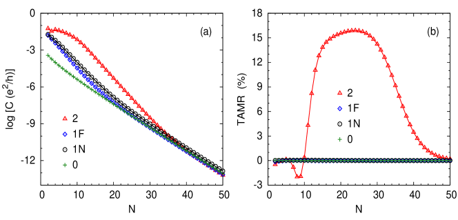
The angular dependence of the conductance is plotted in figure 7 for the case 2 and the barrier thickness . It is seen that the calculated dependence reflects the fourfold symmetry of the system (point group ). The in-plane TAMR is thus defined as the ratio . The dependence of the conductances on the barrier thickness for all four cases and for is shown in figure 8(a). One can see clearly the effect of the resonances, pronounced especially for smaller thicknesses: the straight line for the case 0 is slightly modified by the presence of a single resonance (cases 1F and 1N), whereas the hybridization of two resonances is manifested by a strong enhancement of the conductance (case 2). The corresponding thickness dependences of the TAMR are depicted in figure 8(b). It is seen that a sizeable TAMR effect is obtained only for the case 2 while the single resonances (on either side of the barrier) lead essentially to negligible TAMR values (cases 1F and 1N), similarly to the case 0. The hybridized interface resonances yield also a non-trivial dependence of the TAMR on the barrier thickness: small initial values for are followed by a steep increase to a broad maximum for which is replaced by a final decrease for . This trend is qualitatively similar to that obtained for the Fe/GaAs/Ag system, see figure 4(b).
The different regimes of the thickness dependence of the TAMR can be related to the corresponding -resolved transmissions shown in figure 9 for the case 2 and three values of . For , the total conductances arise from contributions of substantial parts of the whole 2D BZ which leads to a modest TAMR effect for thin tunnelling barriers. For , the dominating contribution to the tunnelling is due to a narrow region (a hot spot), the position of which depends on the angle . The sensitivity of this sharp single local maximum to the angle gives rise to enhanced TAMR values for intermediate barrier thicknesses. For , the hot spots survive but are accompanied by a pronounced peak in the very centre of the 2D BZ, which is reflected by reduced TAMR values for very large insulator thicknesses . This reduction is a simple consequence of vanishing of the Rashba term in the limit of , , see (4). The obtained changes in the -resolved transmissions are in close analogy to the first-principles results, which corroborates the conclusions drawn in section 3.2.
5 Conclusions
The calculated ab initio results for the Fe/GaAs/Ag(001) system with perfect epitaxial interfaces and the properties of a simple tight-binding model of the FM/I/NM junctions demonstrate that hybridized interface resonances can strongly influence the TAMR. In particular, they can lead to sizable TAMR values, especially for intermediate thicknesses of the tunnel barriers. The hybridized interface resonances can be thus added to the list of existing origins of the TAMR: the anisotropic density of states of the FM electrode [6], the interference effects of the Rashba and Dresselhaus contributions to the SO interaction [7, 10], and the interface states at the FM/I interface [11]. This new mechanism – if realized experimentally in a special junction – might also be employed to enhance the TAMR effect for applications in spintronics. Further open problems related to the presented results, such as, e.g., the effect of a finite bias, external magnetic fields or elevated temperatures, remain a task for future studies.
References
References
- [1] S. M. Thompson. J. Phys. D: Appl. Phys., 41:093001, 2008.
- [2] S. D. Bader and S. S. P. Parkin. Annu. Rev. Condens. Matter Phys., 1:71, 2010.
- [3] E. Y. Tsymbal and I. Žutić, editors. Handbook of Spin Transport and Magnetism. CRC Press, Boca Raton, 2012.
- [4] I. M. Miron, G. Gaudin, S. Auffret, B. Rodmacq, A. Schuhl, S. Pizzini, J. Vogel, and P. Gambardella. Nat. Mater., 9:230, 2010.
- [5] B. G. Park, J. Wunderlich, X. Martí, V. Holý, Y. Kurosaki, M. Yamada, H. Yamamoto, A. Nishide, J. Hayakawa, H. Takahashi, A. B. Shick, and T. Jungwirth. Nat. Mater., 10:347, 2011.
- [6] C. Gould, C. Rüster, T. Jungwirth, E. Girgis, G. M. Schott, R. Giraud, K. Brunner, G. Schmidt, and L. W. Molenkamp. Phys. Rev. Lett., 93:117203, 2004.
- [7] J. Moser, A. Matos-Abiague, D. Schuh, W. Wegscheider, J. Fabian, and D. Weiss. Phys. Rev. Lett., 99:056601, 2007.
- [8] A. Manchon. Phys. Rev. B, 83:172403, 2011.
- [9] T. Uemura, M. Harada, T. Akiho, K. Matsuda, and M. Yamamoto. Appl. Phys. Lett., 98:102503, 2011.
- [10] A. Matos-Abiague and J. Fabian. Phys. Rev. B, 79:155303, 2009.
- [11] A. N. Chantis, K. D. Belashchenko, E. Y. Tsymbal, and M. van Schilfgaarde. Phys. Rev. Lett., 98:046601, 2007.
- [12] A. N. Chantis, K. D. Belashchenko, D. L. Smith, E. Y. Tsymbal, M. van Schilfgaarde, and R. C. Albers. Phys. Rev. Lett., 99:196603, 2007.
- [13] H. Ebert, S. Bornemann, J. Braun, D. Ködderitzsch, S. Lowitzer, S. Mankovskyy, J. Minár, M. Offenberger, S. Polesya, and V. Popescu. Psi-k Newsletter, 97:79, 2010. http://www.psi-k.org/newsletters.shtml.
- [14] O. K. Andersen and O. Jepsen. Phys. Rev. Lett., 53:2571, 1984.
- [15] I. Turek, V. Drchal, J. Kudrnovský, M. Šob, and P. Weinberger. Electronic Structure of Disordered Alloys, Surfaces and Interfaces. Kluwer, Boston, 1997.
- [16] I. Turek, J. Kudrnovský, and V. Drchal. In H. Dreyssé, editor, Electronic Structure and Physical Properties of Solids, volume 535 of Lecture Notes in Physics, page 349. Springer, Berlin, 2000.
- [17] S. H. Vosko, L. Wilk, and M. Nusair. Can. J. Phys., 58:1200, 1980.
- [18] I. Turek, K. Carva, and J. Kudrnovský. Advances in Science and Technology, 52:1, 2006.
- [19] T. C. Chiang, J. A. Knapp, M. Aono, and D. E. Eastman. Phys. Rev. B, 21:3513, 1980.
- [20] I. Turek, V. Drchal, and J. Kudrnovský. Philos. Mag., 88:2787, 2008.
- [21] M. E. Rose. Relativistic Electron Theory. John Wiley & Sons, New York, 1961.
- [22] J. Kudrnovský, V. Drchal, C. Blaas, P. Weinberger, I. Turek, and P. Bruno. Phys. Rev. B, 62:15084, 2000.
- [23] K. Carva, I. Turek, J. Kudrnovský, and O. Bengone. Phys. Rev. B, 73:144421, 2006.
- [24] K. Carva and I. Turek. Phys. Rev. B, 80:104432, 2009.
- [25] V. Heine. Group Theory in Quantum Mechanics. Pergamon Press, New York, 1960.
- [26] S. Datta. Electronic Transport in Mesoscopic Systems. Cambridge University Press, 1995.
- [27] G. F. Koster. In F. Seitz and D. Turnbull, editors, Solid State Physics, volume 5, page 173. Academic Press, New York, 1957.
- [28] O. Wunnicke, N. Papanikolaou, R. Zeller, P. H. Dederichs, V. Drchal, and J. Kudrnovský. Phys. Rev. B, 65:064425, 2002.
- [29] K. Xia, P. J. Kelly, G. E. W. Bauer, I. Turek, J. Kudrnovský, and V. Drchal. Phys. Rev. B, 63:064407, 2001.
- [30] V. Drchal, J. Kudrnovský, P. Bruno, P. H. Dederichs, I. Turek, and P. Weinberger. Phys. Rev. B, 65:214414, 2002.
- [31] P. H. Dederichs, P. Mavropoulos, O. Wunnicke, N. Papanikolaou, V. Bellini, R. Zeller, V. Drchal, and J. Kudrnovský. J. Magn. Magn. Mater., 240:108, 2002.
- [32] K. D. Belashchenko, J. Velev, and E. Y. Tsymbal. Phys. Rev. B, 72:140404, 2005.
- [33] E. Y. Tsymbal, K. D. Belashchenko, J. P. Velev, S. S. Jaswal, M. van Schilfgaarde, I. I. Oleynik, and D. A. Stewart. Prog. Mater. Sci., 52:401, 2007.