Macro- and micro-strain in GaN nanowires on Si(111)
Abstract
We analyze the strain state of GaN nanowire ensembles by x-ray diffraction. The nanowires are grown by molecular beam epitaxy on a Si(111) substrate in a self-organized manner. On a macroscopic scale, the nanowires are found to be free of strain. However, coalescence of the nanowires results in micro-strain with a magnitude from to . This micro-strain contributes to the linewidth observed in low-temperature photoluminescence spectra.
pacs:
61.72.Dd, 78.70.Ck, 68.55JkI Introduction
Epitaxially grown semiconductor nanowires (NWs) have attracted large interest in recent years as means to fabricate nano-sized devices. They have been grown using various techniques like e.g. molecular beam epitaxy (MBE) and metal organic chemical vapor phase epitaxy. Often metal catalyst particles are used to initiate the growth. More recently, catalyst-free processes have been developed. The NWs promise to assist in overcoming many of the limitations of heteroepitaxy. Dislocations formed at the NW/substrate interface do not propagate along the NW axis, but remain at the interface or bend toward the free NW sidewalls.Harui et al. (2008); Consonni et al. (2010) Residual strain is released elastically due to the extreme aspect ratio of typical semiconductor NWs.Ertekin et al. (2005); Glas (2006) As a specific example, GaN NWs on Si are virtually free of extended defects despite the very large lattice and thermal mismatch between these materials.Calleja et al. (2000) Furthermore, the spectral position of the donor-bound exciton [(D0,XA)] transition in photoluminescence (PL) spectra of GaN NW ensembles is exactly the same as the one observed in strain free, bulk GaN.Brandt et al. (2010) In apparent contradiction, the linewidth of this transition exceeds values of 1 meV and is thus significantly above the value expected for material free of strain.van Nostrand et al. (2006); Furtmayr et al. (2008); Brandt et al. (2010) Recently, this minimum broadening invariably observed in the PL of GaN NW ensembles has been proposed to arise from the random position of donor sites and the corresponding energy distribution of excitons bound to these donors.Corfdir et al. (2009); Brandt et al. (2010) However, this intrinsic broadening mechanism cannot account for the fact that the linewidth observed for different samples may vary significantly, and may also approach values in excess of the energy separation of the donor-bound exciton transition in the bulk and close to the surface.
Here, we investigate the morphological and structural properties of two GaN NW ensembles on Si(111) exhibiting a PL linewidth differing by more than a factor of two. Using x-ray diffraction (XRD), we determine the orientation distribution of the NW ensembles as well as their strain state. Position and shape of the x-ray diffraction peaks contain information about the strains and sizes as well as the orientation distribution of the NW ensemble. Both samples are found to be entirely relaxed on a macroscopic scale, but to possess a non-negligible micro-strain.
II Experiment
GaN NWs are grown on Si(111) substrates by plasma-assisted MBE. Atomic N and Ga atoms are supplied by a plasma source operating at 500 W and an N2 flux of 2 sccm. Prior to NW growth, the Si substrate is exposed for 5 min to an atomic N flux for nitridation, which results in the formation of a 5 nm thick SixNy film. For sample 1 (2), GaN NWs were subsequently grown for 3 h at a substrate temperature of C and N rich conditions, resulting in NW arrays with an average length of 1.0 (1.6) m.Dogan et al. High-resolution XRD measurements were performed at a temperature of C using a Panalytical X-Pert PRO MRD™ system with a Ge(220) hybrid monochromator (CuK radiation with a wavelength of Å). The circles of the diffractometer are explained in Ref. Fewster and Andrew, 1995. The program Epitaxy™ was used for evaluation of the data. PL spectroscopy was performed using the 325-nm line of a Kimmon He-Cd laser for excitation. The PL signal was dispersed by an 80-cm Horiba Jobin-Yvon monochromator. The spectral resolution of the setup was about 250 eV. The investigations were done at a temperature of 10 K. TEM specimens were prepared by mechanical lapping and polishing, followed by Argon ion milling. TEM images were acquired with a JEOL 3010 microscope operating at 300 kV.
III Results and Discussion
Figures 1(a) and (b) display top-view scanning electron micrographs of samples 1 and 2, respectively. The azimuthal orientation of the NWs, as seen by the direction of their facets, is quite regular although the interfacial SixNy layer is not expected to grow epitaxially. The NWs of sample 2 are distinctly thinner compared to those of sample 1. Coalescence of the NWs is obvious for both samples.
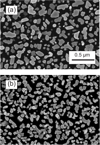
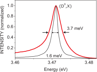
Figure 2 shows near-bandgap PL spectra of the NW ensembles displayed in Fig. 1. For both samples, the dominant line at 3.471 eV is due to the decay of the donor-bound exciton in strain-free GaN.Kornitzer et al. (1999); Wysmolek et al. (2002) Sample 1 exhibits a linewidth of 3.7 meV, more than twice larger than the one observed for sample 2 (1.6 meV). Broadening of bound exciton transitions by their energy dispersion as a function of the distance to the surface is expected to be more important for thin NWs, since the fraction of donors close to the surface increases quadratically with the diameter.Corfdir et al. (2009); Brandt et al. (2010) In the present case, we would thus expect a narrower transition for sample 1 and not a broader one as observed experimentally. Consequently, the additional broadening observed for this sample has a different origin. As hypothesized in the following, a highly probable source of this broadening is microstrain caused by coalescence.
The two samples under investigation were fabricated at different substrate temperatures, which is known to affect both the nucleation density and the lateral growth rate. Lower temperatures as used for sample 1 result in a higher nucleation density as well as a more pronounced tendency towards lateral growth during nucleation, thus resulting in larger nuclei. This scenario will inevitably lead to an enhanced coalescence in an early stage of NW growth, and significantly larger diameters of the final NWs as indeed observed in Fig. 1. The misorientation of the NWs with respect to each other, as well as the dislocations accommodating this misorientation at the tilt or twist boundary,Consonni et al. (2009) will introduce an inhomogeneous elastic distortion of the coalesced aggregate. Simultaneously, the strain introduced at the coalescence junction is more difficult to relax in the thicker NWs of sample 1.Glas (2006) All these arguments would point towards a larger contribution of inhomogeneous strain to the PL linewidth of sample 1, as also observed experimentally. In the following, we examine this hypothesis using high-resolution XRD.
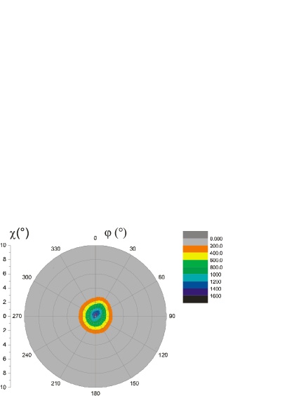
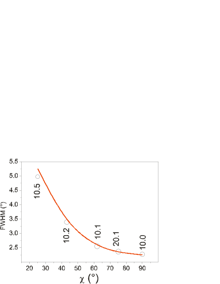
The out-of-plane orientation distribution of the NWs is determined from scans near the GaN 00.4 reflection at several azimuthal orientations. The tilt of [] for sample 1 [2] are typical for GaN NWs grown directly on Si(111). A pole figure of the GaN 00.4 reflection (sample 1) shown in Fig. 3 displays a nearly isotropic angular distribution of the tilt angles of the GaN NWs analogous to a fibre texture. Figure 4 demonstrates the dependence of the full widths at half maximum (FWHM) of the peaks of -scans (circles) performed using different reflections in skew geometry (sample 1) at different tilt angles (see Sun et al. (2002) for a sketch of the skew geometry) including in-plane scans for determination of the range of twist of the NWs. The full line shows the FWHMs extrapolated by:
| (1) |
where is the FWHM of a peak in the -scan for a reflection with a given tilt angle , and is the FWHM of a peak in an in-plane scan revealing the true range of twist of the NWs. Often a -scan can be measured in skew geometry more easily than in an in-plane geometry, then is measured and can be obtained from Eq. (1).
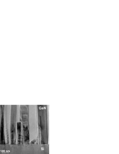
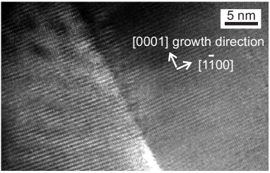
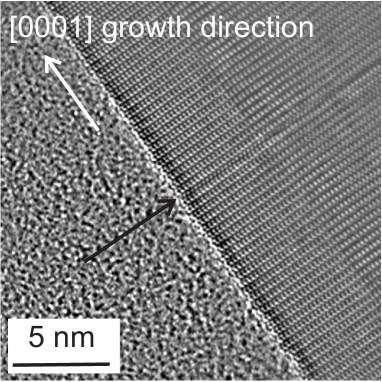
The in-plane orientation distribution of the NWs as obtained from scans of the GaN 10.0 reflection is about [] for sample 1 [2], and is again characteristic for GaN NWs on Si(111). For both samples, coalescence boundaries will be the source of significant strain due to the broad orientation distribution of the NWs. This is illustrated in Figures 5 and 6: Fig. 5 shows a TEM micrograph of the interface region of sample 1, the GaN NWs on the SixNy intermediate film. Strain contrasts are clearly distinguished near the bottom of the NWs and in regions where NWs meet and coalesce. Fig. 6 demonstrates a high-resolution TEM micrograph of the coalesced region of two GaN NWs (sample 1). The border acts as a small angle grain boundary and dislocations are formed in the vicinity to accommodate the tilt. The netplanes are locally curved due to the strain field of the defects. Fig. 7 shows as another example a high-resolution TEM micrograph of an isolated crystal defect in a GaN NW (sample 1). This defect is probably caused by a stacking fault bounded by a dislocation.
To determine the macroscopic strain state of the NWs, we first measured the lattice parameter of our Si substrates by triple-crystal diffractometry Fewster and Andrew (1995); Moram and Vickers (2009). Using an analyzer crystal in front of the detector, the angular positions of the incident and the diffracted beams are determined precisely in order to obtain the Bragg angle. The necessary calculations for the substrate are performed in dynamical approximation Stepanov (1997). We thus obtained a value of Å. Thanks to the small diameter of the NWs, the kinematical approximation is sufficient for the calculation of the angular position of their x-ray reflections. The positions of the symmetrical in-plane and out-of-plane reflections in scans yield (3.1885) Å and (5.1854) Å for the lattice parameters of sample 1 (2). Within the error margin of Å, these values agree with those reported in Refs. Moram and Vickers, 2009 and Robins et al., 2007 for strain-free and pure GaN. This means, that our GaN NWs are indeed free of strain on average.
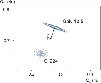
The reciprocal space map shown in Fig. 8 for sample 1 confirms the fully relaxed state of the GaN NWs, because the diffraction vector is pointing in radial direction from the GaN 10.5 peak towards the origin of reciprocal space. The mosaic spread of the GaN NWs can be calculated from the width of the GaN peak perpendicular to the radial direction. The lateral correlation length is calculated from the reciprocal of the FWHM of the GaN 10.5 peak measured parallel to the interface, i.e., along . Here, is the reciprocal lattice unit, where is the corresponding lattice plane distance. From the shape and the orientation of the GaN peak shown in Fig. 8, we obtain a mosaic spread of (i.e., close to the FWHM of the scans) and a lateral correlation length of 76 nm (close to the actual lateral size of the NWs, see Fig. 1).
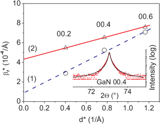
The widths of scans across the GaN 00.n reflections with n increase linearly with the reflection order n, which is the result expected for broadening governed by micro-strain. The line shapes are nearly Lorentzian, so that we obtain the breadth of the physically broadened profile where is the breadth of the apparatus function and that of the measured curve Klug and Alexander (1974). Small asymmetries of the peaks are neglected here. We assume that each GaN NW is a coherently diffracting domain separated by air or a small-angle grain boundary in case of coalescence. These domains are tilted with respect to the interface and twisted around the surface normal by different angles reflected by broad peaks in the and scans. The scans, instead, are broadened due to the finite size of the NWs and due to the inhomogeneous deformations inside the NWs. The integral breadth of the physically broadened line profile is , where is the integral intensity and the peak intensity of the corresponding maximum. We assume that this breadth of our sample consists of size and strain components and . The size component does not depend on the diffraction angle. The strain component grows linearly with the order of reflection Klug and Alexander (1974). We apply the reciprocal lattice notation: is the absolute value of the reciprocal lattice vector and . For a Lorentzian peakshape the two contributions have to be added Langford (2000):
| (2) |
where is the strain.Langford (2000) We can interprete this strain as the variation of spacing within the NWs. The plot of over is expected to give a straight line.Williamson and Hall (1953); Langford (2000) Such a plot shown in Fig. 9 is a Williamson-Hall plot in reciprocal-lattice representation. The intersection with the ordinate axis allows us to determine , corresponding to the size . This is the size of an average domain in the direction of the diffraction vector, i.e., we essentially probe a length along the NWs. The characteristic size is m for sample 1 (2). For sample 1 this length is comparable to the NW length, but for sample 2 it is lower by a factor of five pointing to a smaller domain size inside the wires. The micro-strain () in the GaN NWs of sample 1 (2) is obtained from the slopes of the Williamson-Hall plots. These values describe the fluctuations of the lattice plane distances in the NWs, not their average. We estimate an error of in the determination of the micro-strain. The inhomogeneous micro-strain is caused by residual defects in the GaN NWs like dislocations or even small angle boundaries arising after coalescence of the NWs. Consonni et al. (2009)
The important result obtained here is the fact that the micro-strain for sample 1 is indeed considerably larger than that for sample 2, just as the PL linewidths. A quantitative comparison of these values to the linewidth obtained in PL is, however, not straightforward. Coalescence presumably generates a rather complex strain field, including shear strain, while we only measure the -component of the complete strain tensor. To give an impression of the range of changes of the bandgap by a general strain with , we follow Ref. Gosh et al., 2002 and obtain meV and meV for pure biaxial () and pure hydrostatic () strain, respectively. Considering that at least part of the linewidth is caused by the random distribution of donors and the resulting energy dispersion, it is clear that only a fraction of the strain measured by XRD manifests itself in the linewidth observed in PL. We believe that this finding reflects the presence of dislocations in the coalescence junctions. Dislocations are known to act as nonradiative recombination centers and presumably suppress the PL from the junctions which act as the dominant source of strain measured by XRD.
IV Summary
We have performed structural characterization of MBE grown arrays of GaN NWs on a Si 111 substrate. The average lattice in our GaN NWs is fully relaxed. Typical residual strains in the wires can reach values from to . The local distribution of strain is visible in TEM micrographs. The observed micro-strain contributes to broadening of the lines measured by photoluminescence spectroscopy.
V Acknowledgement
The authors thank U. Jahn for critical reading of the manuscript, A.K. Bluhm for the scanning electron micrographs, A. Pfeiffer and D. Steffen for the preparation of the TEM samples and C. Chéze, V. Kaganer, and L. Geelhaar for helpful discussions.
VI References
References
- Harui et al. (2008) S. Harui, H. Tamiya, T. Akagi, H. Miyake, K. Hiramatsu, T. Araki, and Y. Nanishi, Jap. J. Appl. Phys. 47, 5330 (2008).
- Consonni et al. (2010) V. Consonni, M. Knelangen, L. Geelhaar, A. Trampert, and H. Riechert, Phys. Rev. B 81, 085310 (2010).
- Ertekin et al. (2005) E. Ertekin, P. A. Greaney, D. C. Chrzan, and T. D. Sands, J. Appl. Phys. 97, 114325 (2005).
- Glas (2006) F. Glas, Phys. Rev. B 74, 121302(R) (2006).
- Calleja et al. (2000) E. Calleja, M. A. Sánchez-García, F. J. Sánchez, F. Calle, F. B. Naranjo, E. Muñoz, U. Jahn, and K. H. Ploog, Phys. Rev. B 62, 16826 (2000).
- Brandt et al. (2010) O. Brandt, C. Pfüller, C. Chéze, L. Geelhaar, and H. Riechert, Phys. Rev. B 81, 045302 (2010).
- van Nostrand et al. (2006) J. E. van Nostrand, K. L. Averett, R. Cortez, J. Boeckl, C. E. Stutz, N. A. Sanford, A. V. Davydov, and J. D. Albrecht, J. Cryst. Growth 287, 500 (2006).
- Furtmayr et al. (2008) F. Furtmayr, M. Vielemeyer, M. Stutzmann, A. Laufer, B. K. Meyer, and M. Eickhoff, J. Appl. Phys. 104, 074309 (2008).
- Corfdir et al. (2009) P. Corfdir, P. Lefebvre, J. Ristic, P. Valvin, E. Calleja, A. Trampert, J.-D. Ganière, and B. Deveaud-Plédran, J. Appl. Phys. 105, 013113 (2009).
- (10) P. Dogan, O. Brandt, C. Pfüller, A.-K. Blum, L. Geelhaar, and H. Riechert, J. Cryst. Growth, doi:10.1016/j.jcrysgro.2010.12.081 .
- Fewster and Andrew (1995) P. Fewster and N. Andrew, J. Appl. Cryst. 28, 451 (1995).
- Kornitzer et al. (1999) K. Kornitzer, T. Ebner, M. Grehl, K. Thonke, R. Sauer, C. Kirchner, V. Schwegler, M. Kamp, M. Leszczynski, I. Grzegory, and S. Porowski, Physica Status Solidi B 216, 5 (1999).
- Wysmolek et al. (2002) A. Wysmolek, K. P. Korona, R. Stȩpniewski, J. M. Baranowski, J. Błoniarz, M. Potemski, R. L. Jones, D. C. Look, J. Kuhl, S. S. Park, and S. K. Lee, Phys. Rev. B 66, 245317 (2002).
- Consonni et al. (2009) V. Consonni, M. Knelangen, U. Jahn, A. Trampert, L. Geelhaar, and H. Riechert, Appl. Phys. Lett. 95, 241910 (2009).
- Sun et al. (2002) Y. J. Sun, O. Brandt, T. Y. Liu, A. Trampert, K. H. Ploog, J. Bläsing, and A. Krost, Appl. Phys. Lett. 81, 4928 (2002).
- Moram and Vickers (2009) M. A. Moram and M. E. Vickers, Rep. Prog. Phys. 72, 036502 (2009).
- Stepanov (1997) S. Stepanov, Collection of software (Sergey Stepanov’s X-ray server, http://sergey.gmca.aps.anl.gov/, Chicago, 1997).
- Robins et al. (2007) L. H. Robins, K. A. Bertness, J. M. Barker, N. A. Sanford, and J. B. Schlager, J. Appl. Phys. 101, 113505 (2007).
- Klug and Alexander (1974) H. P. Klug and L. E. Alexander, X-Ray Diffraction procedures (John Wiley, New York, 1974).
- Langford (2000) J. I. Langford, “Industrial applications of x-ray diffraction,” (Marcel Dekker Inc., New York, 2000) p. 751.
- Williamson and Hall (1953) G. K. Williamson and W. H. Hall, Acta Met. 1, 22 (1953).
- Gosh et al. (2002) S. Gosh, P. Waltereit, O. Brandt, H. T. Grahn, and K. H. Ploog, Phys. Rev. B 65, 075202 (2002).