Implementation of low-loss superinductances for quantum circuits
Abstract
The simultaneous suppression of charge fluctuations and offsets is crucial for preserving quantum coherence in devices exploiting large quantum fluctuations of the superconducting phase. This requires an environment with both extremely low DC and high RF impedance. Such an environment is provided by a superinductance, defined as a zero DC resistance inductance whose impedance exceeds the resistance quantum at frequencies of interest (1 - 10 GHz). In addition, the superinductance must have as little dissipation as possible, and possess a self-resonant frequency well above frequencies of interest. The kinetic inductance of an array of Josephson junctions is an ideal candidate to implement the superinductance provided its phase slip rate is sufficiently low. We successfully implemented such an array using large Josephson junctions (), and measured internal losses less than 20 ppm, self-resonant frequencies greater than 10 GHz, and phase slip rates less than 1 mHz.
pacs:
85.25.Cp, 74.81.Fa, 74.50.+r, 64.70.TgThe emerging field of quantum electronics exploiting large fluctuations of the superconducting phase is limited by the practical challenge of engineering an electromagnetic environment which suppresses simultaneously the quantum fluctuations of charge and the random low-frequency fluctuations of offset charges. The small value of the fine structure constant entails a fundamental asymmetry between flux and charge quantum fluctuations, strongly favoring the latter. To illustrate this, let us consider the simplest case of a dissipationless LC oscillator, where the charge on the capacitor plates and the generalized flux across the inductor are conjugate variables. The ratio between quantum fluctuations of charge, , and flux, , in the ground state of the oscillator is given by . Here is the characteristic impedance of the oscillator and is the superconducting resistance quantum. Using only geometrical inductors and capacitors, the characteristic impedance of the oscillator can not exceed the vacuum impedance , thus imposing quantum fluctuations of charge at least an order of magnitude larger than flux fluctuations: .
In order to exceed the vacuum impedance and suppress quantum charge fluctuations, circuit elements with extremely high impedance are required. On chip resistors and long chains of Josephson junctions (JJs) in the dissipative regime have already been used to provide high impedance environments KUZMIN1991 ; Lotkhov2003 ; Corlevi2006 . However, these Ohmic components do not help shunting charge offsets and, being dissipative, they tend to destroy the quantum coherence of the devices. In order to simultaneously suppress quantum charge fluctuations and offsets, we need a circuit element which possesses three key attributes: high impedance at frequencies of interest, perfect conduction at DC and extremely low dissipation. These attributes define the so-called “superinductance” superinductance_Kitaev .
In this Letter, we report the successful implementation and detailed characterization of superinductances using the large kinetic inductance of arrays of Josephson junctions (see Fig 1(a)), following the proof-of-concept shown in the fluxonium circuit Manucharyan2009 . This first superinductance implementation suffered from coherent quantum phases-slips (CQPS) Manucharyan2012 ; Pop2012 , which constitute additional degrees of freedom, difficult to control experimentally. We show that we can completely suppress the CQPS by using large JJs with Josephson energy , where is the charging energy of one junction.
Superconducting nanowires are also likely candidates for implementing superinductances Bezryadin2000 ; Mooij2006 . Unfortunately, they show significant internal dissipation which is not yet well understood, and are more challenging to fabricate. The JJ arrays may also suffer from dissipation, either due to coupling to internal degrees of freedom Fazio2001 ; Rastelli2012 or to a dissipative external bath Lobos2011 . Indeed, transport measurements on large arrays of JJ show the appearance of a superconducting to insulating transition (SIT) with decreasing Josephson energy Chow1998 ; Kuo2001 ; Takahide2006 . Previous implementations of resonators where the inductive energy is given by JJ arrays have yielded internal quality factors in the range of a few thousands Castellanos-Beltrana2007 ; Palacios-Laloy2008 . We show here that the problem of dissipation can be alleviated by using large JJs to realize superinductances far from the SIT region with internal quality factors an order of magnitude above the previously reported values.
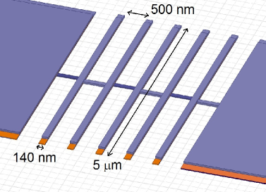
The superinductances are formed by an array of closely spaced Josephson junctions on a C-plane sapphire substrate, as shown in Fig. 1. We fabricated the junctions by e-beam lithography and double angle evaporation of aluminum using the bridge-free technique of BFT ; rigetti . Prior to aluminum deposition, the substrate is cleaned of resist residues using an oxygen plasma pop . We minimize the width of the connecting wires between junctions in order to reduce parasitic capacitances to ground, which ultimately lower the self-resonant frequency of the superinductance hutter2011 .
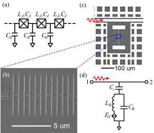
We characterize our superinductances at low temperatures and microwave frequencies by incorporating them in lumped element LC resonators capacitively coupled to a co-planar waveguide in the hanger geometry. The resonator response is measured in transmission. An optical image of a typical device and its low-frequency circuit model are shown in Figs. 1(c,d).
The samples were mounted on the mixing chamber stage (15 mK) of a dilution refrigerator inside a copper box, enclosed in an aluminum-Cryoperm-aluminum shield with a Cryoperm cap. We used two 4-12 GHz Pamtech isolators and a 12 GHz K&L multi-section low-pass filter before the HEMT amplifier, and installed copper powder filters on the input and output lines.
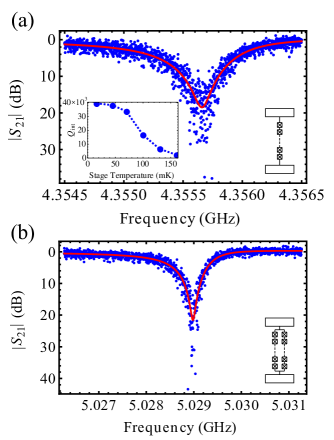
The internal quality factor of a resonator is extracted by fitting the transmission data about the resonance with the response function geerlings
| (1) |
where and are the total and external quality factors, is the resonant frequency, and characterizes asymmetry in the transmission response profile. The internal quality factor is given by . We show a typical measured response for a resonator with an 80-junction superinductance in Fig. 2(a). This yields an internal quality factor of 37,000 for the resonator at 15 mK (stage temperature), corresponding to a loss in the superinductance of better than 27 ppm. We note that an unknown portion of the internal loss comes from the capacitors. The inset of Fig. 2(a) shows the dependence of the internal quality factor on the stage temperature. A similar resonator with two 80-junction arrays in parallel was measured to have a quality factor of 56,000 (Fig. 2(b)), corresponding to a superinductance loss of better than 18 ppm. The external quality factors, , of both resonators were 5,000.
We next evaluate the self-resonant modes of an -junction array. The Lagrangian of the array is
| (2) | |||||
where are the node fluxes associated with each superconducting island. We express each node flux as a superposition of discrete Fourier mode amplitudes,
| (3) |
which leads to a diagonal Hamiltonian of the following form:
| (4) |
Here are the canonical conjugate “charge” variables to the fluxes , and
| (6) |
are respective capacitance and inductance matrices in the Fourier basis. This immediately leads to a dispersion relation of the form,
| (7) |
where is the plasma frequency of a single junction. The coupling capacitance pads at each end of the array (see Fig. 1(c)) load down the eigenfrequencies (see supplementary information for calculation details).
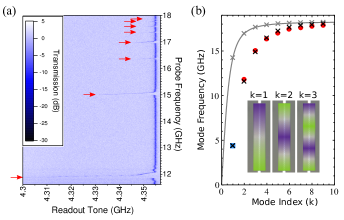
The data presented in Fig. 2 corresponds to measurements of the mode. The frequencies of higher modes, , of the array lie outside the band of our measurement setup. In order to observe these modes we exploit their cross-Kerr interaction, which is induced by the junction nonlinearity. This interaction leads to a frequency shift of the lowest mode () when higher modes are excited. In Fig. 3(a) we show the results of a two-tone measurement of an 80-junction resonator (same device as presented in Fig. 2(a)), where we continuously monitor the mode while sweeping the frequency of a probe tone. When the probe tone is resonant with a higher mode of the array, we observe a drop in the frequency.
Fig. 3(b) shows the comparison between the measured frequencies of the array modes and the theoretically predicted values. The black crosses show the renormalized mode frequencies calculated after incorporation of the corrections due to coupling capacitance pads (see supplementary information), which are in good agreement with the measured frequencies represented by colored markers. The parameters extracted from the fit were fF, fF and nH, with a confidence range of 20%. The simulated value of the capacitance to ground fF agrees within a factor of 2 with the inferred value from the fit. Room temperature resistance measurements of the junction arrays yield a value of nH, which agrees with the fit within 10%. Using the fit parameters we calculate the dispersion relation for the bare superinductance, shown as a gray curve in Fig. 3(b). We note that the lowest resonant frequency of the bare superinductance is 14.2 GHz, which meets the design criterion of having self resonances well above the frequency range of interest (1 - 10 GHz).
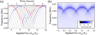
In order to characterize the phase slip rate of the superinductances, we monitor the frequency of the mode of a resonator formed by two superinductances in parallel, while sweeping an external magnetic field. As flux bias is increased, the persistent current induced in the loop increases, and results in a drop in frequency of the mode (Fig. 4(a)). This behavior can be described to lowest order in junction nonlinearity by the quasi-classical expression
| (8) |
where is the applied flux bias, and is the integer number of flux quanta inside the loop. A phase slip event is associated with an integer change in , which we observe as a jump in resonator frequency. As we increase the flux bias, the phase slip rate is enhanced and frequency jumps become more probable mlg . We swept the flux bias applied to the loop over several flux quanta before a phase slip event occurred. The typical duration between phase slips recorded in this experiment was over an hour, Fig. 4(a). This is a remarkably low phase slip rate of well under 1 mHz for a loop of 160 junctions, significantly lower than previously reported values on shorter arrays Manucharyan2012 ; Pop2010 .
Due to the extremely low phase slip rate, in order to measure the resonator in the lowest flux state, we employ an active resetting scheme. We apply a high power pulse at one of the modes before measuring the location of the lowest resonant frequency. This high power pulse activates phase slips, allowing the loop to settle into the lowest flux state. Using this protocol, we tracked the resonant frequency in the lowest flux state, as shown in Fig. 4(b). Discrete inverted parabolas are observed, which allow us to unambiguously calibrate the number of flux quanta in the loop. The fitted value for the total number of junctions differs by 6% from the actual number, which can be explained by the classical nature of the theory which does not take quantum fluctuations into account.
In conclusion, we have demonstrated the successful implementation of superinductances using arrays of Josephson junctions, and performed the first detailed characterization of a superinductance. We measured superinductances in the range of 100–300 nH, self resonant frequencies above 10 GHz, internal losses less than 20 ppm, and phase slip rates below 1 mHz. The long lifetimes of persistent current states in the array loop also demonstrate the low DC resistance of the arrays. With these parameters, the Josephson junction array superinductance enriches significantly the quantum electronics toolbox. Applications would include further suppression of offset charges in superconducting qubits Manucharyan2009 , high Q and tunable lumped-element resonators, on-chip bias tees, kinetic inductance particle detectors Day2003 , and precise measurements of Bloch oscillations bloch .
We would like to acknowledge fruitful discussions with Luigi Frunzio, Kurtis Geerlings, Leonid Glazman, Wiebke Guichard, Zaki Leghtas, Mazyar Mirrahimi, Michael Rooks and Rob Schoelkopf. Facilities use was supported by YINQE and NSF MRSEC DMR 1119826. This research was supported by IARPA under Grant No. W911NF-09-1-0369, ARO under Grant No. W911NF-09-1-0514 and NSF under Grant No. DMR-1006060. As this manuscript was completed, we learned of a similar implementation of a superinductance using a different array topology Bell2012 .
I
Supplemental material for
Implementation of superinductances for quantum circuits
II Simulation of Parasitic Capacitance in Junction Arrays
The parasitic capacitance to ground of the islands in a Josephson junction (JJ) array lowers the self-resonant frequency of the superinductance. We optimize the array geometry in Ansoft Maxwell electromagnetic field simulation software in order to minimize the parasitic capacitance.
Our model for the array includes the connection pads and substrate (Fig. S1(a)). We model the junction oxide layer by a 1 nm thick dielectric material with relative permittivity of 6. Despite only simulating 5 junctions in the array, we can robustly obtain the parasitic capacitance for the full structure. Increasing the number of junctions in the model leads to no significant change in the computed value of the parasitic capacitance.
Numerical simulations revealed that junctions with large, 1:30, aspect ratios minimize the parasitic capacitance (Fig. S1(b)). Fabricating junctions with such large aspect ratios using the Dolan bridge technique is limited by the collapse of the bridge. The bridge-free technique (BFT) rigetti ; BFT allows the fabrication of arbitrary size and aspect ratio junctions. The BFT also minimizes the width of the connecting wires between junctions. Our simulations show that this leads to a reduction of 60% in parasitic capacitance as compared with the standard Dolan bridge technique.
The parasitic capacitance of each island limits the maximum number of junctions in the array to
| (S1) |
a value such that the first self-resonant mode of the array lies 30% below the plasma frequency of a single junction popThesis . In Fig. S1(b) we present a plot of the simulated and as a function of JJ size for large aspect ratio junctions. For our device we obtain .
 |
| (a) |
 |
| (b) |
III Calculating the Scattering Matrix for the Hanger Geometry
In this section we describe the calculation of scattering matrix of an array resonator coupled to a CPW in a hanger geometry. The circuit model is shown in Fig. S2(a), which corresponds to the device shown in Fig. S1(c). Impedance represents the coupling between the CPW feedline and the nearest pad. Impedance represents the cross capacitance between the feedline and the opposite pad, while and represent coupling of the pads to ground. Impedance represents the JJ array.
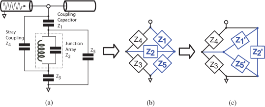
The circuit model in Fig. S2(a) can be simplified by applying the standard Y- transform, as shown in Fig. S2(c). The resulting impedances are given by:
| (S2) | |||||
| (S3) | |||||
| (S4) |
The total impedance of the structure is given by
| (S5) |
We note that the frequency response of near resonance can be approximated using a simplified model as that shown in Fig. 1(d) of the main text. Given the total impedance which shunts the CPW feedline, the scattering matrix can be directly computed using standard techniques Pozar .
IV Details on fabrication procedures
The JJ arrays are fabricated by e-beam lithography at 100 kV using a Vistec 5000+ electron beam pattern generator. The use of a high energy electron beam minimizes forward scattering in the PMMA/MMA resist bilayer and allows implementation of a bridge-free double angle evaporation technique BFT . We develop using a mixture 1:3 of IPA:water at 6 ∘C. Prior to aluminum deposition, the substrate is cleaned of resist residues using a high pressure, low power oxygen plasma pop . The aluminum films are deposited in a Plassys UMS300 UHV multichamber e-beam evaporation system with a base pressure of Torr. The static oxidation in between the aluminum layer depositions is performed in a separate chamber, in a mixture 1:3 of :Ar at 100 Torr for 10 minutes. We obtain critical current densities of the order of tens of amperes per square centimeter. The junctions age by 10% during the first week after fabrication.
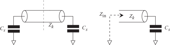
V Modification of array mode frequencies by coupling pad capacitances
The end capacitance pads lower the eigenmodes of the JJ array. To evaluate the modified mode frequencies of the -junction array , we model each mode as a transmission line of characteristic impedance,
| (S6) | |||||
terminated by a shunt capacitance at both ends. Here k represents the reduced superconducting resistance quantum (Fig. S3).
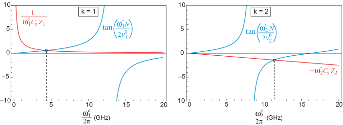
In order to calculate a mode frequency of the loaded transmission line, we exploit the symmetry of the problem by considering a half-section of the line. The input impedance of each section can be written as Pozar
| (S7) |
where and denotes the wave number associated with the mode. At resonance frequency , the impedances of left and right sections of the transmission line satisfy the identity . Further, due to symmetry, the input impedances of the left and right sections of the transmission line are equal, . These two conditions imply , which leads to a relationship,
| (S8) |
Here denotes the phase velocity for each mode evaluated using the unloaded array calculation. Equation (S8) is a transcendental equation in , which can be solved numerically for each of the modes to obtain the corrected mode frequency. The above calculation yields the corrected mode frequencies only for the odd modes of the array. Similar treatment using the input admittance yields the corrected frequencies for the even modes, as solutions of the following transcendental equation
| (S9) |
Fig. S4 shows example calculations for the first two mode frequencies using the method described above.
References
- (1) L. S. Kuzmin and D. B. Haviland, Physical Review Letters 67, 2890 (1991)
- (2) S. V. Lotkhov, S. A. Bogoslovsky, A. B. Zorin, and J. Niemeyer, Phys. Rev. Lett. 91, 197002 (2003)
- (3) S. Corlevi, W. Guichard, F. W. J. Hekking, and D. B. Haviland, Physical Review Letters 97, 096802 (2006)
- (4) Term introduced by A. Kitaev (unpublished)
- (5) V. E. Manucharyan, J. Koch, L. I. Glazman, and M. H. Devoret, Science 326, 113 (Oct. 2009)
- (6) V. E. Manucharyan, N. A. Masluk, A. Kamal, J. Koch, L. I. Glazman, and M. H. Devoret, Phys. Rev. B 85, 024521 (2012)
- (7) I. M. Pop, B. Douçot, L. Ioffe, I. Protopopov, F. Lecocq, I. Matei, O. Buisson, and W. Guichard, Phys. Rev. B 85, 094503 (Mar. 2012)
- (8) A. Bezryadin, C. N. Lau, and M. Tinkham, Nature 404, 971 (2000)
- (9) J. E. Mooij and Y. V. Nazarov, Nature Physics 2, 169 (Mar. 2006)
- (10) R. Fazio and H. van der Zant, Physics Reports-review Section of Physics Letters 355, 235 (2001)
- (11) G. Rastelli, I. M. Pop, W. Guichard, and F. W. J. Hekking, ArXiv e-prints 1201.0539v1(Jan. 2012), arXiv:1201.0539 [cond-mat.supr-con]
- (12) A. M. Lobos and T. Giamarchi, Phys. Rev. B 84, 024523 (2011)
- (13) E. Chow, P. Delsing, and D. B. Haviland, Physical Review Letters 81, 204 (1998)
- (14) W. Kuo and C. D. Chen, Phys. Rev. Lett. 87, 186804 (2001)
- (15) Y. Takahide, H. Miyazaki, and Y. Ootuka, Physical Review B 73, 224503 (Jun. 2006)
- (16) M. A. Castellanos-Beltran and K. W. Lehnert, Applied Physics Letters 91, 083509 (2007)
- (17) A. Palacios-Laloy, F. Nguyen, F. Mallet, P. Bertet, D. Vion, and D. Esteve, Journal of Low Temperature Physics 151, 1034 (May 2008)
- (18) F. Lecocq, I. M. Pop, Z. Peng, I. Matei, T. Crozes, T. Fournier, C. Naud, W. Guichard, and O. Buisson, Nanotechnology 22, 315302 (2011)
- (19) C. T. Rigetti, Quantum Gates for Superconducting Qubits, Ph.D. thesis, Yale University, New Haven, Connecticut (2009)
- (20) I. M. Pop, T. Fournier, T. Crozes, F. Lecocq, I. Matei, B. Pannetier, O. Buisson, and W. Guichard, Journal of Vacuum Science & Technology B: Microelectronics and Nanometer Structures 30, 010607 (2012)
- (21) C. Hutter, E. A. Tholén, K. Stannigel, J. Lidmar, and D. B. Haviland, Phys. Rev. B 83, 014511 (2011)
- (22) K. Geerlings, S. Shankar, E. Edwards, L. Frunzio, R. J. Schoelkopf, and M. H. Devoret, Applied Physics Letters 100, 192601 (2012)
- (23) Pop, I. et al., in preparation
- (24) K. A. Matveev, A. I. Larkin, and L. I. Glazman, Phys. Rev. Lett. 89, 096802 (2002)
- (25) I. M. Pop, I. Protopopov, F. Lecocq, Z. Peng, B. Pannetier, O. Buisson, and W. Guichard, Nature Physics 6, 589 (2010)
- (26) P. K. Day, H. G. LeDuc, B. A. Mazin, A. Vayonakis, and J. Zmuidzinas, Nature 425, 817 (2003)
- (27) W. Guichard and F. W. J. Hekking, Phys. Rev. B 81, 064508 (2010)
- (28) M. T. Bell, I. A. Sadovskyy, L. B. Ioffe, A. Y. Kitaev, and M. E. Gershenson, ArXiv e-prints(Jun. 2012), arXiv:1206.0307 [cond-mat.supr-con]
- (29) I. M. Pop, Quantum Phase-Slips in Josephson Junction Chains, Ph.D. thesis, Université de Grenoble, Grenoble, France (2011)
- (30) D. M. Pozar, Microwave Engineering (3rd edition) (Wiley, 2005)