Quantum spin/valley Hall effect and topological insulator phase transitions in silicene
Abstract
We present a theoretical realization of quantum spin and quantum valley Hall effects in silicene. We show that combination of an electric field and intrinsic spin-orbit interaction leads to quantum phase transitions at the charge neutrality point. This phase transition from a two dimensional topological insulator to a trivial insulating state is accompanied by a quenching of the quantum spin Hall effect and the onset of a quantum valley Hall effect, providing a tool to experimentally tune the topological state of silicene. In contrast to graphene and other conventional topological insulators, the proposed effects in silicene are accessible to experiments.
pacs:
71.90.+q,73.43.-f,73.22.-f,71.70.Ej,85.75.-dSilicene is a single layer of silicon 1 ; 2 isostructural to graphene 3 . It has a low buckled honeycomb structure, where the charge carriers behave like massless Dirac fermions 4 . Experimental realizations of silicene sheets 4 ; 5 and ribbons 6 ; 7 have been demonstrated by synthesis on metal surfaces. It is believed that silicene can be the starting point of new opportunities for electrically tunable electronic devices, in alternative to graphene 8 . Though graphene possesses extraordinary properties 3 , its application in device fabrication is limited by the zero band gap and the difficulty to tune Dirac particles electrically. Moreover, even if a gap can be introduced in graphene by chemical doping it is incompatible with existing nanoelectronics. In the desire to overcome this limitation, the buckling in silicene offers new possibilities for manipulating the particle dispersion to achieve an electrically tunable band gap. In addition to the electric field controlled gap, silicene has a relatively large intrinsic spin-orbit interaction (SOI) induced gap of 1.55 meV 9 , which provides a mass to the Dirac fermions. This mass can be controlled experimentally by applying an external perpendicular electric field. Recently, the SOI gap in silicene has been studied using density functional band structure calculations 9 , predicting a quantum spin Hall effect (QSHE) in an experimentally accessible temperature regime, in contrast to graphene 10 ; 11 ; 12 ; 13 .
The QSHE has attracted significant interest in condensed matter physics as it constitutes a new phase of matter 10 ; 14 ; 15 ; 16 ; 17 ; 18 ; 19 ; 20 ; 21a . Therefore, when Kane and Mele 10 in a ground breaking study of graphene proposed a new class of insulators, the topological insulators, a great theoretical 17 ; 18 ; 19 ; 20 ; 21a and experimental excitement was generated 15 ; 16 ; 19 . These materials are insulating in the bulk, whereas the surface states are conducting and protected against scattering by time reversal symmetry. The surface states are chiral and have a well defined spin texture with a single Dirac cone energy spectrum. The occurrence of conducting surface states is related to SOI 19 , which is a crucial criterion for realizing the QSHE. It was proposed to search for new materials with strong SOI for the fabrication of spintronic devices 10 ; 19 . In addition to the QSHE, an analogous quantum valley Hall effect (QVHE) 21a ; 21b arises from a broken inversion symmetry, where Dirac fermions in different valleys flow to opposite transverse edges when an in-plane electric field is applied in presence of intrinsic SOI. The QVHE paves the way to electric generation and detection of valley polarization.
In the light of the above discussion, silicene is likely to show significant signatures of QSHE and QVHE, as well as a transition from a topologically trivial to a band insulating state and further to a semimetallic state. The QSHE and QVHE are the fundamental transport processes arising from intrinsic SOI and an external perpendicular electric field, respectively. The latter can give rise to a topologically nontrivial band insulator or semimetal, leading to a quantized Hall and valley conductivity without magnetic field. Here we show that the quantum phase transition from a two dimensional topological insulator to a trivial insulating state is accompanied by a quenching of the QSHE and the onset of a QVHE, providing a tool to experimentally tune the topological state of silicene. We consider silicene in the presence of an external electric field and intrinsic SOI to discuss these phenomena, disregarding the extrinsic SOI as it is weak (0.7 meV) with respect to the intrinsic SOI (3.9 meV) 22 ; 23 . We employ the standard Kubo formalism to derive the Hall conductivity, which is experimentally accessible at reasonable temperatures due to the remarkable buckling and strong SOI in silicene. We believe that our results open new experimental directions for the realization of the QSHE, QVHE, and topological insulators.
Dirac fermions in buckled silicene obey the two-dimensional graphene-like Hamiltonian 8 ; 22 ; 23
| (1) |
Here, for , , where is the uniform electric field applied perpendicular to the silicene sheet with Å, (, , ) is the vector of Pauli matrices, and denotes the Fermi velocity of the Dirac fermions. Spin up () and down () is represented by and , respectively. After diagonalizing the Hamiltonian given in Eq. (1), we obtain the eigenvalues
| (2) |
Here, denotes the electron/hole band, and the absolute value of the wave vector is given by . The corresponding eigenfunctions for the K point with spin up are
| (3) |
and
| (4) |
with and . The corresponding solutions for the K point with spin down are
| (5) |
and
| (6) |
The eigenfunctions for the point can be obtained by exchanging spin up and down in the point solution with replaced by .
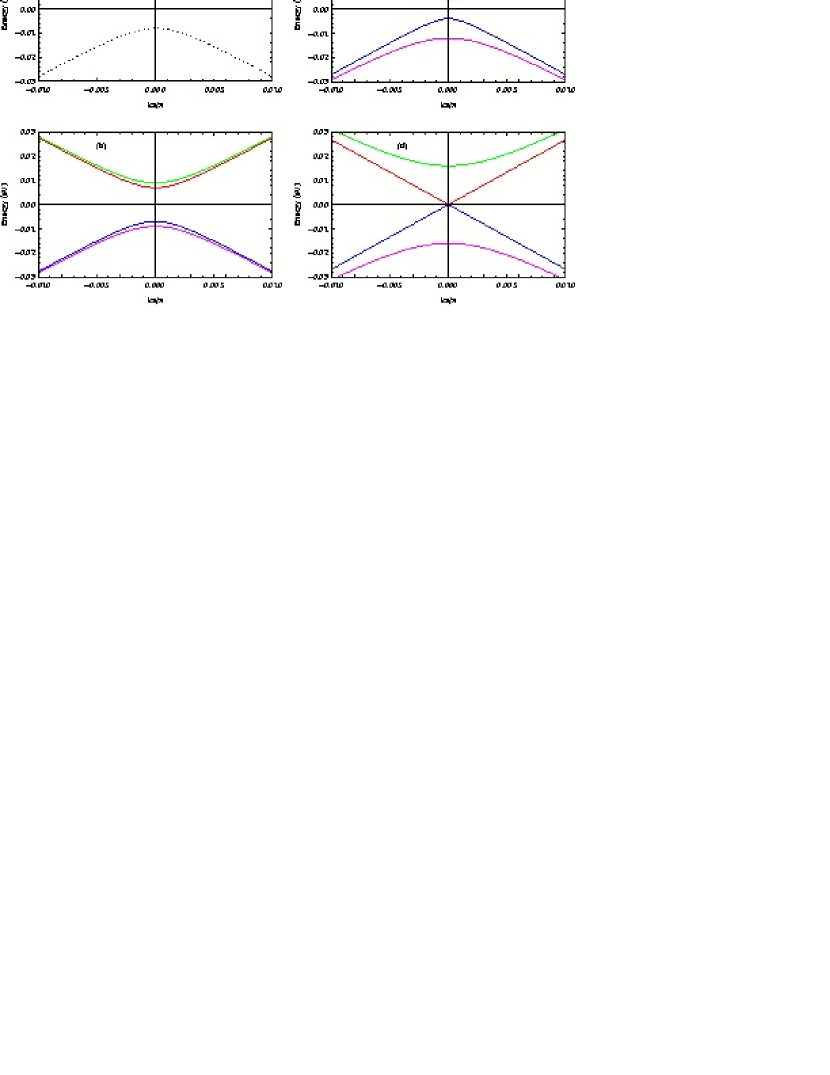
First we discuss the energy eigenvalues obtained in Eq. (2) for the point to explore the band splitting and quantum phase transitions. The energy is plotted as a function of dimensionless wave number () in Fig. 1 for a lattice constant of Å. In Fig. 1(a) we find a well resolved energy gap for either the electric field or the SOI finite. This confirms a metal to insulator transition. Figure 1(b) for finite SOI and perpendicular external electric field with shows an energy splitting between the spin up and down bands of both the electrons and holes. This splitting is less than the energy gap between the electrons and holes. The situation reflects a topological insulating state. Figure 1(c) is analogous to Fig. 1(b) but for . The splitting of the spin up bands remains the same as in Fig. 1(b), while the splitting of the spin down bands increases. This situation corresponds to a band insulator. Figure 1(d) is analogous to Figs. 1(b) and (c) but for . We see that the energy gap closes between the spin up bands, while the spin down bands maintain a finite energy gap. This reflects a semimetallic state 24 ; 25 ; 26 ; 27 . Note that for the point the eigenvalues are identical to those of the point if spin up and down are exchanged.
The Hall conductivity can be obtained by the standard Kubo formula as 10 ; 20
| (7) |
The velocity components and can be obtained from the Hamiltonian in Eq. (1). Using Eqs. (2) to (6), the expectation values of the velocities are derived and used in Eq. (7). We arrive at
| (8) |
If the Fermi level lies in the gap we can write the conductivity given in Eq. (8) for zero temperature as
| (9) |
Evaluating the integral in Eq. (9), we obtain the spin and valley Hall conductivities as
From Eqs. (10) and (11) we see that the Hall conductivity for the and points is not degenerate. This confirms the lifting of the valley (,) degeneracy (known for graphene) in silicene 10 ; 19 ; 20 . In conventional insulators there is only a single valley. When then and , which corresponds to the topological insulating state 10 . When then and , which corresponds to a trivial insulator 21a . This means that there is a finite Hall conductivity even when the Fermi level is inside the band gap, implying the presence of gapless helical edge states. This situation can be regarded as a quantum spin Hall state. On the other hand, when the signs of and are different then and there are no edge states. This corresponds to the case of a topologically trivial insulator.
We turn to the situation when the Fermi level is in the valence or conduction band. Now, Eq. (8) yields
| (12) |
After performing the integral in Eq. (12) and applying the integration limit we obtain
| (13) |
Finally, the spin and valley Hall conductivities for the Fermi level in the conduction band at zero temperature can be written as
| (14) |
| (15) |
Equations (14) and (15) show that the and points are not degenerate. We obtain similar results for the case when the Fermi level lies in the valence band due to the electron-hole symmetry. A closer analytical examination of Eqs. (14) and (15) implies that silicene is subject to quantum phase transitions as shown and discussed in Fig. 1.
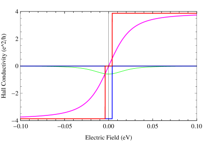
We show in Fig. 2 the quantum spin and valley Hall conductivities as functions of the electric field for a fixed value of the SOI. By tuning the electric field one may tune the SHE and VHE. The transition is striking in the case of the QSHE and QVHE (i.e., the Fermi level is in the gap). However, also in the realistic case when the Fermi level is above or below the gap it is possible to observe this topological transition. For comparison with existing work, if we assume that the perpendicular electric field is zero () our results are similar to those obtained for the QSHE in graphene and conventional systems 10 ; 19 ; 20 . However, in silicene the SOI is much stronger and should be accessible experimentally at reasonable temperatures. Further, with the inclusion of the SOI becomes more pronounced, giving rise to a finite mass term. The opposite signs of the terms in the spin up and down channels of the effective Hamiltonian lift the spin and valley degeneracies. This distinguishes silicene from graphene and is responsible for the quantum phase transitions from a topological insulator to a band insulator and further to a semimetal. Such a general mechanism is not possible in graphene and conventional topological insulators with perpendicular electric field, while it is guaranteed in silicene by the two opposite spins and valleys.
The Hamiltonian in Eq. (1) can also be used to describe germanene, which is a honeycomb structure of germanium 4 ; 9 ; 22 . Here the SOI is even stronger ( meV) with Å. Hence, the above analysis is fully applicable to germanene. Our results imply that the SOI splitting can be controlled by a gate voltage or external electric field. This is of significance for electrically tunable spintronics devices 20 , especially Datta-Das spin field-effect transistors 28 . Therefore, realization of the QSHE, QVHE, and quantum phase transitions in silicene and germanene topological insulators provides new spintronic materials for high efficiency electric spin manipulation.
To conclude, we have carried out analytical calculations for the Hall conductivity in silicene, based on the Kubo formula. An electric field is included to take into account the effect of electrical tuning for nanoelectronic applications. In an insulator where the chemical potential is located inside the energy gap between the conduction and valence bands the Hall conductivity is an integer multiple of . The calculated Hall conductivity of silicene jumps from 1 to 0 at the critical electric field of the level crossing. Experimentally, the best way to see the QSHE and QVHE is to measure the Hall conductivity as a function of the gate voltage (that tunes the chemical potential). A plateau in the Hall conductivity should be observed when the chemical potential is inside the gap. In silicene and germanene, the temperature will not affect the Hall plateau as the SOI is strong. It is shown that the energy splitting due to the SOI and electric field leads to QSHE and QVHE with quantum phase transitions at the charge neutrality point. Thus QSHE, QVHE, and the topological insulating states in silicene and germanene can be observed experimentally at finite temperature.
References
- (1) K. Takeda and K. Shiraishi, Phys. Rev. B 50, 14916 (1994).
- (2) G. G. Guzmán-Verri and L. C. Lew Yan Voon, Phys. Rev. B 76, 075131 (2007).
- (3) A. K. Geim, Science 324, 1530 (2009); A. H. Castro Neto, F. Guinea, N. M. R. Peres, K. S. Novoselov, and A. K. Geim, Rev. Mod. Phys. 81, 109 (2009).
- (4) P. Vogt, P. D. Padova, C. Quaresima, J. Avila, E. Frantzeskakis, M. C. Asensio, A. Resta, B. Ealet, and G. L. Lay, Phys. Rev. Lett. 108, 155501 (2012).
- (5) B. Lalmi, H. Oughaddou, H. Enriquez, A. Kara, S. Vizzini, B. Ealet, and B. Aufray, Appl. Phys. Lett. 97, 223109 (2010).
- (6) B. Aufray, A. Kara, S. Vizzini, H. Oughaddou, C. Léandri, B. Ealet, and G. L. Lay, Appl. Phys. Lett. 96, 183102 (2010).
- (7) P. E. Padova, C. Quaresima, C. Ottaviani, P. M. Sheverdyaeva, P. Moras, C. Carbone, D. Topwal, B. Olivieri, A. Kara, H. Oughaddou, B. Aufray, and G. L. Lay, Appl. Phys. Lett. 96, 261905 (2010).
- (8) N. D. Drummond, V. Zólyomi, and V. I. Fal’ko, Phys. Rev. B 85, 075423 (2012).
- (9) C. C. Liu, W. Feng, and Y. Yao, Phys. Rev. Lett. 107, 076802 (2011).
- (10) C. L. Kane and E. J. Mele, Phys. Rev. Lett. 95, 226801 (2005).
- (11) Y. G. Yao, F. Ye, X. L. Qi, S. C. Zhang, and Z. Fang, Phys. Rev. B 75, 041401(R) (2007).
- (12) D. Huertas-Hernando, F. Guinea, and A. Brataas, Phys. Rev. B 74, 155426 (2006).
- (13) H. Min, J. E. Hill, N. A. Sinitsyn, B. R. Sahu, and L. Kleinman, A. H. MacDonald, Phys. Rev. B 74, 165310 (2006).
- (14) C. L. Kane and E. J. Mele, Phys. Rev. Lett. 95, 146802 (2005).
- (15) B. A. Bernevig, T. L. Hughes, and S. C. Zhang, Science 314, 1757 (2006).
- (16) M. König, S. Wiedmann, C. Brüne, A. Roth, H. Buhmann, L. W. Molenkamp, X. L. Qi, and S. C. Zhang, Science 318, 766 (2007).
- (17) S. Murakami, Phys. Rev. Lett. 97, 236805 (2006).
- (18) C. X. Liu, T. L. Hughes, X. L. Qi, K. Wang, and S. C. Zhang, Phys. Rev. Lett. 100, 236601 (2008).
- (19) D. Pesin and A. H. MacDonald, Nat. Mat. 11, 409 (2012).
- (20) N. A. Sinitsyn, J. E. Hill, H. Min, J. Sinova, and A. H. MacDonald, Phys. Rev. Lett. 97, 106804 (2006).
- (21) D. Xiao, W. Yao, and Q. Niu, Phys. Rev. Lett. 99, 236809 (2007).
- (22) A. Rycerz, J. Tworzydlo, and C. W. J. Beenakker, Nat. Phys. 3, 172 (2007).
- (23) C. C. Liu, H. Jiang, and Y. Yao, Phys. Rev. B 84, 195430 (2011).
- (24) M. Ezawa, New J. Phys. 14, 03303 (2012).
- (25) M. Z. Hasan and C. L. Kane, Rev. Mod. Phys. 82, 3045 (2010).
- (26) X.-L. Qi and S.-C. Zhang, Rev. Mod. Phys. 83, 1057 (2011).
- (27) Y. Xia, D. Qian, D. Hsieh, L. Wray, A. Pal, H. Lin, A. Bansil, D. Grauer, Y. S. Hor, R. J. Cava, and M. Z. Hasan, Nat. Phys. 5, 398 (2009).
- (28) Z. Wang, Y. Sun, X. Q. Chen, C. Franchini, G. Xu, H. Weng, X. Dai, and Z. Fang, Phys. Rev. B 85, 195320 (2012).
- (29) S. Datta and B. Das, Appl. Phys. Lett. 56, 665 (1990).