11institutetext:
Area de Física Teórica y Materia Condensada, UAM-Azcapotzalco,
Avenida San Pablo 180, Código Postal 02200 México Distrito Federal,
México
Spin polarized field effect transistors
Solutions of wave equations: bound states
Spin-orbit coupling, Zeeman and Stark splitting, Jahn-Teller effect
Engineering a spin-fet: spin-orbit phenomena and spin transport induced by a gate electric field
J. L. Cardoso and H. Hernández-Saldaña
Abstract
In this work, we show that a gate electric field, applied in the base of the field-effect devices, leads to inducing spin-orbit interactions (Rashba and linear Dresselhauss) and confines the transport electrons in a two-dimensional electron gas. On the basis of these phenomena we solve analytically the Pauli equation when the Rashba strength and the linear Dresselhaus one are equal, for a tuning value of the gate electric field . Using the transfer matrix approach, we provide a joint description of the transport by varying the bias electric field, . We can flip the spin of the incident electrons, or block the spin-down completely. The robustness of this behavior is proved when changes by .
pacs:
85.75.Hh
pacs:
03.65.Ge
pacs:
71.70.Ej
1 Introduction
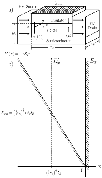
The main consequences of the nanometer-scale devices, with defined boundary conditions, are the confinement of the electric carriers in one-dimensional potential wells and the formation of discrete energy spectra. For example, when an homogeneous magnetic field is applied in a nanostructure, the energy levels are defined by the well-known Landau levels and the associated spectrum can be manipulated by this magnetic field [1]. For a gate electric field, there are two approaches for studying its influence in a two-dimensional electron gas (2DEG) spectrum: with perturbation methods [2, 3, 4] or with Airy functions [5, 6, 7]. We found the quantization of the transverse energy of the electron, the thickness of the 2DEG and, hence, the induction of the spin-orbit interactions, by taking into account the exactly solvable problem whose solutions are linear combinations of two independent Bessel- functions and simulate the gate junction as an infinity triangular potential well for an idealized Spin-FET, see fig. 1 a) and b).
The manipulation of spin by electric fields in semiconducting environments has generated a lot of theoretical and experimental research aimed at developing useful spintronic devices and novel physical concepts [8, 9]. The spin transistor elucidated by Datta and Das[10] is made to drive a modulated spin-polarized current. For this, the spin precession is controlled via the Rashba spin-orbit coupling associated with the interfacial electric fields present in the quantum well that contains the 2DEG. The strength of this interaction can be tuned by the application of an external gate voltage [11, 12, 13, 14]. The linear Dresselhaus spin-orbit interaction (SOI) could be induced by a gate electric field [7, 15, 16, 17, 18]. This work shows how the gate electric field can tune the Rashba and linear Dresselhaus strengths and the interplay between them. For gate electric field value where the interplay is equal to and its neighborhood, we study the spin transport of the 2DEG in the base by solving analytically the Pauli equation and build the corresponding transfer matrix.
2 The 2DEG and the SOI terms induced by a gate electric field
In this section, we shall study how the gate electric field, , works on the base. It quantizes, with the appropriate boundary conditions, the transverse energy of the electrons, it induces the spin-orbit interactions and the creation the 2DEG. In fig. 1 a), it is shown an idealized spin-FET, with a semiconductor base’s dimensions , and and two ferromagnetic materials as the source and the drain. We ignore the magnetic field caused by the ferromagnetic contacts. The source-to-drain electric field in the direction, , is weaker; hence, we neglect its influence to induce any SOI in our approach.
Figure 1: a) An idealized Spin-FET with base’s dimensions , and . We consider here that is oriented along the crystallographic axis . A 2DEG at the plane will be formed into the base when a gate electric field is applied and it has a thickness given by the average position . b) The gate electric field provokes a confinement due to a triangular potential well for . A bound wave-function itself must vanish outside of the triangular well and at the endpoints and .
In order to study the influence of the gate electric field, we take into account the one-dimensional Schrödinger equation
(1)
where is the effective mass, is the electron charge and is the transverse energy. It is well-known that the solution of this equation is given by the linear combination of the Bessel- functions with , and . Several electrons can be trapped in the base, when the gate electric field is applied. In order to understand the electric field’s confinement on the base, we take into account a triangular potential well formed by for and for , as shown in Fig. 1 b), this model is equivalent to the used ones in refs. [5, 6, 7]. The bound states inside of this triangular potential can be determined if we consider the following boundary conditions and . The most general solution of the one dimensional Schrödinger equation, satisfying the first condition, is of the form . On the other hand, the second boundary condition implies that and . Hence nontrivial solutions of this problem exist only if has a value such that , here is the th-root of the Bessel- function, i. e. . In this way, the -bound state acquires the energy . Geometrically, a bound wave-function itself must vanish outside the triangular well and at the endpoints and , see Fig. 1 b). Taking into account a shift of the zero of the -coordinate, we can write the boundary conditions, , the one-dimensional Schrödinger equation (1) is reduced and has the following structure: . The average squared momentum can be calculated with the previous equation . By using the boundary conditions and and considering a Sturm-Liouville problem, we can calculate the average position
(2)
With the change of variable , the previous integrals can be written as
(3)
The integral of the denominator has a well-known value, , while the integral of the numerator is calculated with the help of the following indefinite integral when and . In this way, and, therefore, the average squared momentum is written by . A 2DEG at the plane will be formed into the base when a gate electric field is applied and it has a thickness given by the average position . This thickness is numerically equivalent to the one given in [7] for the ground state, . This thickness decreases monotonically when grows, but its magnitude increases for higher values of ; this implies that the 2DEG is created only by small root values and high gate electric fields.
Figure 2: Interplay as a function of the gate electric field. In plot a) GaAs and the roots , and . The Dresselhaus strength increases with large values of and the Rashba one does not. When the Rashba SOI dominates the behavior of the 2DEG, while the behavior of the 2DEG is given by the Dresselhaus term. Plot b) shows the interplay as a function of for three conventional III-V semiconductors InSb, InAs and GaSb at the ground state . The dominant SOI in the InSb is the Rashba term, while the GaSb has a strong Dresselhaus one. The SOI terms of the InAs behave similarly as the GaAs does.
We consider here that both SOI are induced by the gate electric field . If the geometry of the base is such that for an applied gate electric field, it is possible that the inequalities can be true, where the sub-index gc means geometrical confinement and, for example, for the grown state. In the effective-mass approximation, the electron Hamiltonian of a zinc-blendes structure has a spin-dependent coupling called the Dresselhaus term [19], , where is the Dresselhaus three dimensional term, and with , and the components of the momentum and the Pauli matrices respectively. For the triangular potential well and the -direction, which is consider parallel to crystallographic direction , the Dresselhaus term is reduced to . We propose that the most important term of the linear Dresselhaus interaction is written by , with . For a spin-FET where the linear Dresselhaus strength could be given by ; in this work we neglect the geometrical confinement. [20, 21, 22] consider only the geometrical confinement because . On the other hand, the Rashba interaction [23] has the following form , with and the material’s constant. The ratio denotes the interplay between the Rashba strength and the linear Dresselhaus one. Such interplay is given by the following expression
(4)
it is a function of the electric field and depends parametrically on the root and the semiconductor nature (, and , table 1 has those values). By varying the gate electric field, one can modulate this interplay. Figure 2a) shows the interplay for GaAs, graphed in the interval at the roots , and . grows monotonically with the gate electric field for a fixed root . The horizontal dotted line point up when . If we take into account the curve we can find that for a value of the gate electric field, , inside the considered interval, but for and these fields are too large. In other words, the Dresselhaus strength increases with large values of and the Rashba does not. When the Rashba SOI dominates the behavior of the 2DEG, while the behavior of the 2DEG is given by the Dresselhaus term. Figure 2b) shows the interplay as a function of for three conventional zinc-blende semiconductors InSb, InAs and GaSb at the ground state . The curve of the interplay for InSb is over 1, while the corresponding curve of the GaSb is below 1. In this way, the dominant SOI in the InSb is the Rashba term, while the GaSb has a strong Dresselhaus one. The SOI terms of the InAs behave similarly as the GaAs does. Those analitical calculus generalizes the numerical results of ref. [7].
Table 1: Physical properties of the zinc-blende structure semiconductors, according with ref. [7]
Semiconductor
GaAs
0.0670
4.4
26
InSb
0.0136
500
228
InAs
0.0239
110
130
GaSb
0.0412
33
187
3 The transport of the 2DEG under induced spin-orbit interaction
Into the base, several electrons can be trapped by the gate electric field and they form a 2DEG, which is moving in the plane under the influence of the induced SOI terms. This movement is described by the Pauli equation with SOI
(5)
where is the Hamiltonian, is the momentum, is the effective mass, is the bias electric field (), is the Fermi energy and and are the Rashba and the Dresselhaus strengths respectively and is the transverse confining hard wall potential ( for and infinite outside this potential region). According to [24], the time reversal operator is anti-linear, i. e. , and it has the following structure , with the complex-conjugation operator. The Hamiltonian with SOI terms is invariant under time reversal, . Thus, this Hamiltonian can not produce spontaneous spin polarization [12]. To get rid of the variable , we will consider the complete set of stationary states of a particle in an -dimensional triangular potential well with . In other words, we can use these functions to express the wave function in the form
(6)
where the expansion coefficients are spinors. If we introduce this function in the Pauli equation (5), we have
(7)
here , and . The degrees of freedom of the axis are completely separated from those in the plane. This problem can be considered then as a two-dimensional one and its solutions depend parametrically on . We choose the confinement along to be much stronger, for high gate electric fields, such that only the lowest subband (given by ) is occupied in this direction under all operating conditions. We only look for solutions around , other modes can be solved in a similar way. For clarity, the index shall be suppressed in the following expressions. In order to get rid of the variable , we will consider the complete set of stationary states of a particle in a -dimensional infinite potential well with boundary conditions , which are solutions of the differential equation
It is easy to verify that , where , and are spinors, for odd and for even, , and is a rotation operator. If we use the complete set of functions to expand , we get . By introducing this function in the Pauli equation (7), multiplying by and integrating on the variable , we have
(8)
here , , , and the mixing terms are given by and . Notice that if the previous equations are uncoupled; in ref. [20] a similar case is studied. However, this symmetry would be broken with a magnetic field pointing in any direction.
According to fig. 2 a) for the GaAs [fig. 2 b) for the InAs], the value of the gate electric field () gives the interplay . If we take values in the neighborhood of , where , it is possible to show that and the eq. (8) can be reduced in the first approximation
(9)
The coupling terms are not significant and, therefore, they can be negligible and the previous coupled eqs. become the following system of uncoupled eqs.
(10)
For each wavenumber , there are two propagating physical channels: one with spin-up and another with spin-down. The general solutions of these equations are given by being , , and and are spinors. We now match the wave function and its derivative at the borders of the base region. In this way, we can connect the incident waves (to the left-hand side of the source) with the outgoing ones (to the right-hand of the drain). The evolution of the spin- state vectors is governed by the two-channel transfer matrix
(11)
where
and are just the derivatives of and with respect to and is the unit matrix. This transfer matrix has the symplectic structure[24]
(12)
with . Given we are ready to calculate the whole Spin-FET transmission amplitude
(13)
where (here and label the spin-up () or spin-down () projections) is the transmission amplitude from channel on the source to channel on the drain, and is the (1,1) block of the spin-FET transfer matrix . The off-diagonal terms and are the transmission amplitudes for processes where an odd number of spin flips have taken place inside the base. The corresponding transmission coefficients are defined by .
Figure 3: Transmission coefficients as functions of the bias electric field. In the panel a) we have the transmission coefficients and , while in the panel b) we have the transmission coefficients and . By varying , the transmission can be modulated more efficiently: we can flip the spin of the incident electrons, or block the spin-down completely, and thus establish a spin transistor.
We consider electrons of energy injected into a base structure, with for . In this report, we will keep fixed the following geometrical variables: and . We are interested here on the visualization of spin-transitions based on the transmission coefficients. We shall start considering the effect of varying the bias electric field on the transmission coefficients, we can then use it as a tuning spin-transition parameter. In the panel a) of fig. 3 we have the transmission coefficients and , while in the panel b) we have the transmission coefficients and .
It is easy to see the influence of the rotation operator , not only on the well known shifting between and , but also on the spin transition processes. The shifting phenomena is given by influence, while the spin transition depends on . The general trend of and is oscillatory. The minimum values of are around zero and the minimum values of are not. The transmission coefficients and , exhibit the oscillatory behavior of the two uncoupled-spin transmission coefficients. These maximum and minimum reflect the passage of flux from one spin state to another. The origin of these transitions is the precession term of , which stimulates a mixing between the propagating physical channels. The minimum values of and are close to zero too. Here, we show that by varying , the transmission can be modulated more efficiently: we can flip the spin of the incident electrons, or block the spin-down completely, and thus establish a spin transistor.
Figure 4: Transmission coefficients as functions of the bias electric field. In panel a) , and are plotted for , in panel b) , and are plot-ed for . The general trends discussed in fig. 3 are preserved and, especially, one can modulate them by varying the bias electric field.
An important question is how robust the results are if we change the value of the gate electric field by , where . In fig. 4 we plot the transmission coefficients as function of the bias electric field: in panel a) , and are plotted for , in panel b) , and are plotted for . As shown there, the transmission curves are not always perfect: the minimum values of are not zero and their position change. However, the general trends discussed in fig. 3 are preserved and, especially, one can modulate them by varying the bias electric field.
All of the results presented so far are valid when only a single Fourier mode propagates in the base. If more modes are allowed to mix, when and with a magnetic field, the coefficient transmissions pattern become more complex but it is still possible to have an analytical solution by using the Sylvester Theorem for matrix-valued functions for solving the Pauli eq. Details will be given elsewhere. In ref. [3] was discussed the multichannel transmission coefficients for a FET system using this approach where the SOI is not relevant.
In summary, we combined the spin precession in the base of a spin-FET, due to the induced spin-orbit coupling, with the analytical solution of the Pauli eq., and applied it to calculate the transfer matrix at the base. We showed that we can select the spin of the outgoing electrons to be the same as or opposite to that of the injected spin polarized electrons. More important, we can have a nearly binary square-wave transmission spin-valve effect͒ for the spin-up orientation.
Acknowledgements.
The authors would like to thank Professor J. Gravinsky, for clarifying discussions.
References
[1]\NameTsui D. C. \REVIEWRev. Mod. Phys. 711999891 and references
therein.
[2]\NameBastard G., Mendez E. E., Chang L. L. Esaki L. \REVIEWPhys. Rev. B 2819833241.
[3]\NamePereyra P. Anzaldo-Meneses A. \REVIEWMicroelectronics J.
362005419.
[4]\NameAlves F. M., Marques G. E., Lopez-Richard V. Trallero-Giner C.
\REVIEWSemicond. Sci. Technol. 222007301.
[5]\NameMiller D. A. B., Chemla D. S., Damen T. C., Gossard A. C., Wiegmann W.,
Wood T. H. Burrus C. A. \REVIEWPhys. Rev. Lett 5319842173.
[6]\NameMiller D. A. B., Chemla D. S., Damen T. C., Gossard A. C., Wiegmann W.,
Wood T. H. Burrus C. A. \REVIEWPhys. Rev. B 3219851043.
[7]\Namede Sousa R. Sarma D. \REVIEWPhys. Rev. B 682004155330.
[8]\NameZ̆utić I., Fabian J. Sharma S. D. \REVIEWRev. Mod. Phys.
762004323.
[9]\NameBandyopadhyay S. Cahay M. \BookIntroduction to Spintronics (CRC
Press) 2008.
[10]\NameDatta S. Das B. \REVIEWAppl. Phys. Lett 561990665.
[11]\NameNitta J., Akazaki T., Takayanagi H. Enoki T. \REVIEWPhys. Rev. Lett. 7819971335.
[12]\NameMireles F. Kirczenow G. \REVIEWPhys. Rev. B 642001024426.
[13]\NameMiller J. B., Zumbuhl D., Marcus C., Lyanda-Geller Y., Goldhaber-Gordon
D., Campman K. Gossard A. \REVIEWPhys. Rev. Lett.
902003076807.
[14]\NameJiang Y. Jalil M. \REVIEWJ. Phys.: Condens. Matter
152003L31.
[15]\NamePrabhakar S. Raynolds J. E. \REVIEWPhys. Rev. B
792009195307.
[16]\NamePrabhakar S., Raynolds J. E., Inomata A. Melnik R. \REVIEWPhys. Rev. B 822010195306.
[17]\NameBandyopadhyay S. Cahay M. \REVIEWAppl. Phys. Lett.
8420041814.
[18]\NameGujarathi S., Alam K. M. Pramanik S. \REVIEWPhys. Rev. B
852012045413.
[19]\NameDresselhaus G. \REVIEWPhys. Rev. 1001955580.
[20]\NameSchliemann J., Egues J. C. Loss D. \REVIEWPhys. Rev. Lett
902003146801.
[21]\NameXu W. Guo Y. \REVIEWPhysics Letters A 3402005281.
[22]\NameOhno M. Yoh K. \REVIEWPhys. Rev. B 772008045323.
[23]\NameRashba E. I. \REVIEWSoviet Physics-Solid State 11959368.
[24]\NamePereyra P. \REVIEWJ. Math. Phys. 3619951166.