Exchange engineering in 3d chains adsorbed on Cu2N/Cu(001)
Abstract
Covalent substrates can give rise to a variety of magnetic interaction mechanisms among adsorbed transition metal atoms building atomic nanostructures. We show this by calculating the ground state magnetic configuration of monoatomic chains deposited on a monolayer of Cu2N grown on Cu(001) as a function of filling and of adsorption sites of the one dimensional nanostructures.
I Introduction
The study of the interactions which underlie the magnetic ground state of deposited nanostructures constitutes an area of enormous interest nowadays, both, in applied and in basic research. The systems of interest can be atomically manipulated and deposited on different substrates by means of scanning tunneling microcopy (STM). For future spintronic applications the search is, among others, towards adequate films able to decouple the deposited nanostructures from the underlying metallic substrate, diminishing as much as possible the influence of the latter on the electronic and magnetic properties of adsorbed nano-objects. Actually, isolation is never complete and, the decoupling layers themselves play, in principle, a role to be determined on the magnetic interactions of the nanostructures.
Copper nitride overlayers grown on different Cu surfaces have been recently used as decoupling systems, being it possible to develop stable thin films even at the monolayer thickness, while preserving an ordered geometric structure. Actually, the number of systems which fulfill these conditions seems to be limited and, thereafter, copper nitride monolayers, called from now on Cu2N, are currently being investigated both theoretically as experimentally.Stampfl ; Gupta1 ; Gupta2
Focusing on the magnetic interactions within the nanostructures, Mn chains of different lengths have been deposited by Hirjibehedin et al Hirjibehedin on Cu2N/Cu(001) at different adsorption sites by doing manipulation with an STM. Performing inelastic electron tunneling spectroscopy (IETS) the authors concluded that the interatomic Mn-Mn interactions are antiferromagnetic with an interaction strength which depends on the deposition configuration. There have been different theoretical contributions addressing these interactions.jones ; nuestro1 ; nuestro2 ; Jones_Ti ; Jones_Lin ; Scopel In particular, in previous works we have studied the effect of the surrounding geometry on the magnetic interatomic interactions for Mn and Cr chains deposited on Cu2N/Cu(001).nuestro1 ; nuestro2
Recently the group of R. Wiesendanger has proposed to make use of the RKKY interaction among Fe adatoms deposited on a non magnetic metallic susbstrate, namely, the (111) surface of a copper monocrystal, to fabricate spin-based logic devices.wiesendanger In fact, this group has achieved it to realize and develop a model system able to perform logic operations. The tip of an STM was used to deposit chains of antiferromagnetically coupled Fe adatoms and, using spin polarized scanning-tunneling spectroscopy (SP-STS), the magnetic interaction among the spins of the deposited adatoms was measured. The designed model device was able to transmit and process certain desired magnetic information. The authors suggest that combinations of antiferromagnetic and ferromagnetically coupled chains could be used to realize new model gates by properly tuning the interatomic distances of the adsorbed atoms.
In this contribution we show that using covalent decoupling layers, such as the Cu2N monolayers grown on Cu(001), it is possible to obtain different intrachain magnetic interactions for an adsorbed atomic chain with a given filling. This can be achieved not by tuning the interatomic distance of the adsorbed nanostructures but, by changing the adsorption sites of the transition metal atoms, which could be part of an eventual spintronic device. The richness provided by the molecular substrate lies in the fact that the interatomic interactions within the deposited chains can change dramatically not only as a funtion of -filling but also depending on adsorption configuration, while keeping the distance among chain atoms fixed.
We present the results of a systematic study of the behaviour of the magnetic interactions within Cr, Mn, Fe and Co chains deposited on the above mentioned molecular system. Four different chain adsorption geometries are considered, geometries which involve different magnetic mediation processes, with the aim of highlighting the effect of the local and crystal environment on the interacting orbitals of the chains. We find that the adsorption sites of the chain atoms on the decoupling layer determine the kind of magnetic interaction involved, while the filling of the -orbitals determines the final magnetic ground state.
II Calculation Details
We perform ab initio calculations based on density functional theory (DFT) using the full potential linearized augmented plane waves method (FP-LAPW), as implemented in the WIEN2k code.wien The generalized gradient approximation (GGA) for the exchange and correlation potential in the parametrization of Perdew, Burke and Ernzerhof perdew and the augmented plane wave-local orbital (apw-lo) basis are used. The cutoff parameter which gives the number of plane waves in the interstitial region is taken as , where is the value of the largest reciprocal lattice vector used in the plane waves’ expansion and is the smallest muffin tin radio used. The number of points in the Brillouin zone is enough in each case to obtain the desired energy and charge precision, namely Ry and e respectively.
The nitrogen atoms of the pristine substrate occupy fourfold coordinated hollow sites on the outermost metallic copper layer, forming a c(2x2) local structure.Leibsle This structure forms islands on the Cu(001) surface and, as mentioned in the introduction, the chains are built atom by atom on one of these Cu2N islands. We simulate an island by considering a Cu2N monolayer on Cu(001). This system is modeled with a supercell composed by a five layers slab separated by a vacuum region of 13.8 Å. The thickness of the vacuum region is found to be sufficiently large to avoid interactions among subsequent slabs. To exploit inversion symmetry and to prevent unphysical multipoles, each slab has one Cu2N monolayer on each side.
The surface lattice constant follows pseudomorphically the underlying Cu(001) substrate and we use the experimental lattice constant of copper. We consider that the adsorbed 3 atomic chains are infinite long and they are deposited on both sides of the slabs. The nearest neighbour 3-3 distance along the chains is 3.61 Å in all the cases studied. In these supercell calculations, chains are periodically arranged 7.2 Å apart from each other assuming that the interchain interactions are much smaller than the intrachain ones.
The positions of all atoms in the supercell of the proposed systems are allowed to move until forces are smaller than 0.1 eV/Å.
III Calculations and Results
III.1 The different surface structures
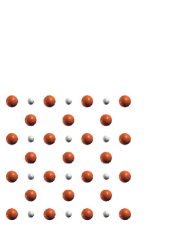
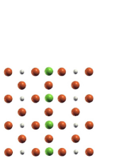
For Cr, Mn, Fe and Co chains, we consider four different stable adsorption geometries. Fig. 1 (a) displays a schematic top view of the Cu2N/Cu(001) substrate, while the different geometric chain configurations are depicted in Fig. 1 (b-e).
In the first adsorption geometry, the 3 chains are arranged directly on top of Cu atoms of the Cu2N monolayer, in such a way that one N atom of the nitride lies inbetween each pair of atoms along the chain. There are four lateral copper atoms of the Cu2N monolayer surrounding each chain atom. This is one of the experimentally reported situationsHirjibehedin and we call it s1. See Fig. 1(b).
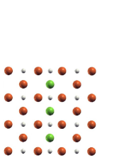
In the second geometry, s2, each atom of the chain is deposited, as in the case of s1, on top of Cu atoms but now every chain atom is laterally surrounded by two nitrogens, one at each side in the direction perpendicular to the chain, as shown in Fig. 1 (c). There are also four lateral copper atoms of the Cu2N substrate surrounding each chain atom.
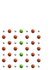
In the third case, called the s3 arrangement, the 3 atoms are located in hollow sites of the Cu2N layer, as it is shown in Fig. 1(d). There are four surface Cu atoms and four nitrogens around each 3 one.
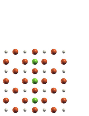
The last configuration considered, the s4, is one in which the 3 atoms sit on top of nitrogens of the substrate as depicted in Fig. 1 (e). Each 3 atom is surrounded by four coppers of the underlying substrate. This configuration has also been experimentally reported. Hirjibehedin
|
|
|
|
|
| ( a) | (b) | (c) | (d) | (e) |
Due to the reduced coordination number and the covalent nature of the underlying Cu2N network, the local atomic environment should play, a priori, a relevant role on the final electronic and magnetic structure of the deposited chains, being it important to properly optimize them. We relax the different systems by starting always from the ferromagnetic spin configuration of the chain arrangement.
For the different 3 fillings the final relaxed positions within each configuration are very similar, the differences among them being at most of 0.1 Å. In the s1 geometry the N atoms, which are inbetween two 3 ones, change significantly their vertical distance with respect to the Cu2N layer, relaxing outwards and forming a nearly linear diatomic chain together with the 3 atoms. These last ones lie slightly higher (0.1 Å) than the N atoms, the bond length between them is around 1.8 Å for all fillings considered. This is in agreement with previous results.jones The Cu atoms just below the diatomic chain are second nearest neighbors of the 3 ones. The distance between them lies in the range 2.3-2.4 Å. There are four Cu atoms on the surface layer which are third nearest neighbours to a 3 one at 2.7-2.8 Å distance.
When relaxing the s2 structure, the two lateral N atoms of each 3 one move towards the chains forming N-3 bonds of lengths lying in the range 1.8-1.9 Å. The distance between the 3 transition metal atoms and the Cu atom directly beneath them ends up being, after relaxation, of 2.3-2.4 Å. There are four lateral copper atoms at 2.9 Å from each 3 one.
The effect of relaxing the atomic positions in the s3 configuration is that each 3 atom ends up having, in the Cu2N monolayer, four copper atoms at 2.4-2.6 Å and four nitrogens at 2.5 Å . The copper atom beneath each 3 one, which belongs to the metallic Cu(001) substrate is at 3.4-3.5 Å of the corresponding chain atom.
In the case of the s4 structure the distance between each 3 chain atom and the nitrogen sitting directly below, ranges from 1.7 Å to 1.8 Å depending on filling. In this case the N atoms move away from the Cu2N monolayer towards the chain and the four nearest copper atoms are at 3.0-3.1 Å distance from each chain atom.
In all the adsorption geometries considered, the N atoms closest to the chains have a tendency to relax towards the transition metal chain atoms.
III.2 Bonding and electronic structure.
The electronic density distribution of the systems under study depends on the adsorption sites of the chains. It determines the type of bonding and, as it will be seen in the next section, also the nature of the magnetic interactions.
Analyzing the electronic density distribution, we find that there are three different ways in which the considered adsorbed 3 chains bind to the substrate: i) forming a diatomic covalent one dimensional nanostructure "metalically" bonded to the substrate, ii) building a monoatomic chain which binds covalently to the substrate and, iii) building a monoatomic chain which binds metalically to the substrate.
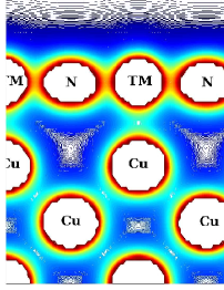
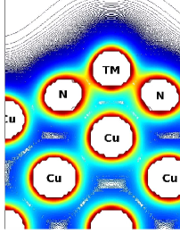
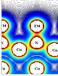
In Fig. 2 we present electronic charge density plots for the s1 system along planes: (a) containing the deposited chain and (b) perpendicular to it and going through a chain atom. The s1 structure shows 1D covalent bonding among each 3 atoms and the N ones which build the diatomic chain. The binding to the substrate of this covalent chain is achieved through copper atoms which originally belonged to the pristine Cu2N monolayer and that now sit below the 3 atoms of the chain. This binding can be considered as "metallic-like" when compared with the charge distribution inbetween Cu atoms of a Cu substrate. The bonding in this case belongs to type i).
|
|

|
| ( a) | (b) |
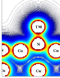
In the s2 configuration, the 3 chains are covalently bonded to the substrate through the two nitrogen atoms lying lateral to each chain one. These nitrogen atoms remain being covalently bonded to the original monolayer. This can be concluded from Fig. 3, where electronic density plots for different planes are being shown. In Fig. 3 (a) the selected plane contains a 3 chain and is perpendicular to the surface. In Fig. 3 (b) the plane is perpendicular to the chain and shows that the N atoms on each side, lateral to a chain atom, form covalent bonds with it. We are then in the presence of a type ii) bonding.
|
|

|
| ( a) | (b) |
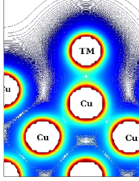
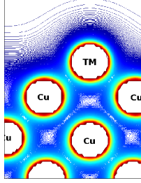
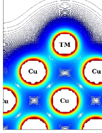
In the s3 structure the adsorbed 3 chain sits in a metallic-like channel of the surrounding Cu2N monolayer, the channel being built by the copper atoms nearest to the chain (case iii). The bond is metallic like as it can be observed in Fig. 4. Fig. 4 (a) displays the electronic density along a plane which contains the 3 chain and is perpendicular to the surface and Fig. 4 (b) shows it in a plane perpendicular to the chain which contains one 3 atom. The local environment of the transition metal atoms is similar to the one they have when adsorbed directly on Cu(001). Just for comparison, we present in Fig. 5 the electronic density distribution along and perpendicular to a 3 chain absorbed on holes of the Cu(001) surface. We call this last system s5 and it is clear that the environment of the chain in s3 and s5 is very similar. We have checked that there is no covalent bond between the chain atoms and their neighboring nitrogens and this strengthens the fact that the chain presents only metallic bonds with its surroundings.
|
|
|

|
| ( a) | (b) |

|
|
|
| ( a) | (b) |
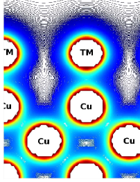
In the s4 configuration the 3 chain is covalently bonded to the Cu2N substrate through the nitrogen atom sitting below each chain atom. This can be observed in the electronic density plots of Fig. 6. Fig. 6 (a) presents a plane containing the 3 chain, which is perpendicular to the surface and Fig. 6 (b) shows a plane perpendicular to the chain and to the surface, which goes through one atom of the chain. The binding in this arrangement is clearly of type ii).
|
|

|
| ( a) | (b) |
All the electronic density plots shown in this work are for Mn chains, but no relevant differences are observed for the other fillings.
Summarizing in s1, s2 and s4 the 3 atoms of the chains are covalently bonded to their nearest neighbor nitrogen atoms, but, in s1 the chain binds metalically to the substrate, while in s2 and s4 it does it covalently. On the other hand, in s3 the 3 chain is metalically bonded to the Cu2N substrate.
III.3 Magnetic configurations
As stated in the introduction, among the possible magnetic solutions, we consider only collinear ferromagnetic (FM) and antiferromagnetic (AFM) ones for each atomic adsorption configuration. We are aware of the fact that in those cases in which the difference in energy between the FM and AFM magnetic order is small, other interactions could turn out being important and that the ground state might be non collinear, but, in this work we are mainly concerned with general trends.
In order to analyse the evolution of the magnetic ground state as a function of band filling and adsorption sites of the chains, we calculate the difference in energy, , between the AFM and FM configurations for all the arrangements. If this difference is negative the magnetic ground state is AFM, if not, it is FM. The results obtained for s1, s2, s3 and s4 appear in Fig. 7. As it can be seen s1 has a completely different magnetic behaviour than the other three configurations. In s1 the magnetic interaction goes from FM to AFM with increasing filling, while the reverse is observed for s2 and s4, both, presenting similar trends. As discussed in the previous section, in the s2 and s4 arrangements the 3 atoms are covalently bonded to neighboring nitrogens, but in s1 there is a nitrogen atom inbetween two 3 ones. The nitrogen atom in the diatomic chain gives rise to a superexchange like magnetic coupling among the 3 atoms. This kind of adsorption situation, which enables this nitrogen mediated interaction, has already been treated in the literature for Mn chains and for several dimers.Jones_Ti ; Jones_Lin ; Scopel
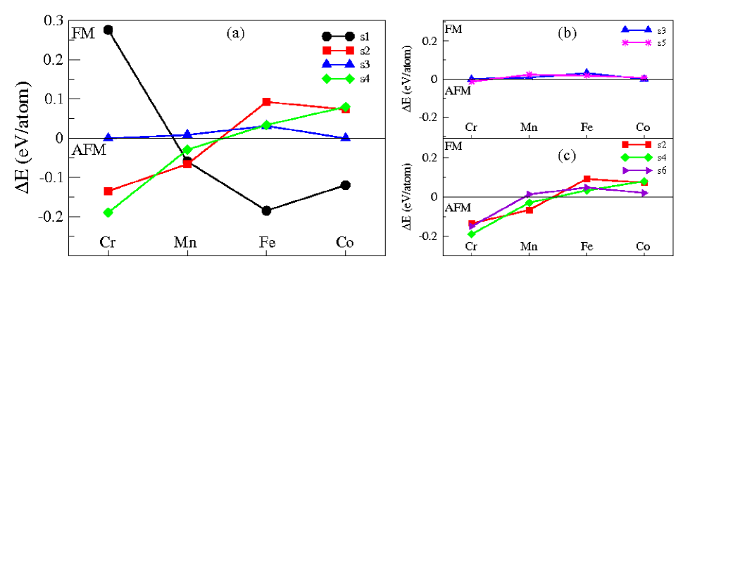
In s2 and s4 the atoms of the 3 chains are covalently bonded to the substrate through their neighboring nitrogen atoms and in both cases the magnetic ground states go from AFM to FM as a function of filling. There is a direct exchange interaction along the chains and an indirect interaction through the substrate. The question is which is more significant. If one compares the results for obtained in the case of the s2 and s4 configurations with those corresponding to the unsupported chains at the same interatomic distance, s6, the same trends for the magnetic interaction are found as a function of filling. The energy differences between ferro- and antiferromagnetic configurations are also of the same order of magnitude. The results for for the unsupported chains together with those corresponding to s2 and s4 are presented in Fig 7 (c). These results show that the direct interaction among the 3 atoms is comparable in the three cases. This is also apparent from the comparison of the electronic density plots of Fig 3 (a) and Fig 6 (a) with that of an unsupported chain at the same interatomic distance. The indirect interaction through the substrate is certainly affecting the energy difference for each particular filling, giving rise to a switching of the solution from FM to AFM in the case of Mn. In the case of Mn the direct interaction is small and competes with the other interactions at the considered interatomic distance, but it does not change the general trends.
Finally, s3 presents a different behavior as a function of filling when compared with the other configurations and the results for point towards the preponderance of another type of magnetic interaction. The difference in energy , in this case, evolves as if the chains were adsorbed directly on hollow sites of Cu(001), that is, the so called s5 configuration. This is clear from Fig 7 (b) where we compare for s3 and s5 and from which it is seen that the order of magnitude and the sign of is the same for the four filling studied. In the s3 arrangement the interaction among atoms of the 3 chains seems to be predominantly RKKY-like, as it is the case when 3 atoms are directly adsorbed on Cu(111).Wiensendanger
It is interesting to compare our results with those obtained for the exchange coupling among Ti atoms in Ref. Jones_Ti, when depositing a monolayer of titanium on the same Cu2N/Cu(001)surface. The coupling obtained by the authors along an N axis and along a hollow axis are to be compared with the exchange energies obtained by us in the s1 and s2 configurations of the deposited chains. Following the trends already discussed, for Ti chains in the s1 and s2 configurations we would have obtained also ferromagnetic and antiferromagnetic exchange couplings, respectively.
IV Conclusions
Summarizing, the covalently bonded nitride substrate Cu2N offers an interesting template to taylor magnetic interactions among transition metal atoms by taking as variable the adsorption sites. We have shown this by depositing chains on four different adsorption sites with the same interatomic distance among 3 atoms and for four different fillings. Due to the different type of bonding present, we obtain that the atoms interact magnetically through completely different mechanisms depending on adsorption geometry. For a given filling, the interaction can be strongly AFM or FM for the same interatomic distance along the chain. This versatility could be very promising regarding the future possibility of making spin engineering at the nanometer scale. We expect a similar richness in the magnetic interactions, when using other covalently bonded substrates.
Acknowledgments
MAB is supported and MCU and AML are partially supported by CONICET and belong to the Institute if nanoscience and Nanotechnology (INN) of the Atomic Energy Agency (CNEA), Argentina. This work was partially funded by the grants PIP No 11220090100258 (CONICET), UBACYT-X123 (UBA), PICT R1776 (ANPCyT) and PRH 2077 No 74 (ANPCyT).
References
- (1) A. Soon, L. Wong, B. Delley and C. Stampfl, Phys. Rev. B 77, 125423 (2008).
- (2) T. Choi, C.D. Ruggiero and J.A. Gupta, Phys. Rev. B 78, 035430 (2008).
- (3) C.D. Ruggiero, T. Choi and J. Gupta, Appl. Phys. Lett 91, 253016 (2007).
- (4) C.Hirjibehedin, C. Lutz, and A. Heinrich, Science 312, 1021 (2006).
- (5) C. F. Hirjibehedin, Chiung-Yuan Lin, A. F. Otte,M. Ternes, C. P. Lutz, B. A. Jones and A. J. Heinrich, Science 317, 1199 (2007).
- (6) M.C. Urdaniz, M.A. Barral and A.M. Llois, Physica B 404,2822 (2009).
- (7) M.A. Barral, R. Weht, G. Lozano and A.M. Llois, Physica B 398, 369 (2007).
- (8) R. Pushpa, J. Cruz, and B. Jones, Phys. Rev. B 84, 075422 (2011).
- (9) C.Y Lin and B.A Jones, Phys. Rev. B 83, 014413 (2011).
- (10) W.L. Scopel, P. Venezuela and R.B. Muniz, Phys. Rev. B 79, 132403 (2009).
- (11) A.Khajetoorians, J.Wiebe, B.Chilian, and R.Wiesendanger, Science 332, 6033 (2011)
- (12) P. Blaha, K. Schwarz, G.K.H. Madsen, D. Kvasnicka and J. Luitz, WIEN2k, An Augmented Plane Wave + Local Orbitals Program for Calculating Crystal Properties (Karlheinz Schwarz, Techn. Universitat Wien, Austria), 2001. ISBN 3-9501031-1-2
- (13) J. P. Perdew and Y. Wang, Phys. Rev. B 45, 13244 (1992).
- (14) F.M. Leibsle, C.F.J. Flipse, and A.W. Robinson, Phys. Rev. B 47, 15865 (1993)
- (15) A. Khajatoorians, J. Wielse, B. Chilian, S. Louis, S. Blugel, and R. Wiensendanger, Nature Physics 8, 497 (2012).
- (16) V.I. Anisimov, I.V. Solovyev, M.A. Korotin, M.T. Czyzyk, and G.A. Sawatzky, Phys. Rev. B 48, 16929 (1993).
- (17) A.I. Liechtenstein, V.I. Anisimov, J. Zaanen, Phys. Rev. B 52, R5467 (1995).