Electron-hole pairing in topological insulator thin film
Abstract
We consider pairing of massless Dirac electrons and holes located on opposite surfaces of thin film of “strong” three-dimensional topological insulator. Such pairing was predicted to give rise to topological exciton condensate with unusual properties. We estimate quantitatively achievable critical temperature of the pairing with taking into account self-consistent screening of the Coulomb interaction, disorder and hybridization of electron and hole states caused by a tunneling through the film. Increase of the gap above the hybridization value when the temperature is lowered can be observable signature of the pairing. System parameters required to observe the electron-hole pairing are discussed.
pacs:
71.35.-y, 73.20.-r, 73.22.GkI Introduction
Research of nontrivial topological states of matter was highly stimulated in recent years by discovery of two- and three-dimensional topological insulators (TIs) Hasan ; Qi1 . Nonzero topological invariant characterizing global topology of filled electron states in Hilbert space across the whole Brillouin zone distinguishes TI from a trivial insulator. One of the most interesting properties of TI is the existence of gapless topologically protected edge (in a two-dimensional case) or surface (in a three-dimensional case) electron states.
Unusual properties of surface modes manifest themselves most strikingly in second generation of “strong” three-dimensional TIs represented by such materials as , , , and others ZhangLiu ; Hsieh ; Chen1 ; Xia . In these materials band structure of the surface states contains a Dirac cone, and electrons obey a two-dimensional Dirac-Weyl equation for massless particles in the vicinity of a Dirac point. Electrons in graphene demonstrate similar properties but have two inequivalent Dirac cones and additional two-fold degeneracy by spin projections CastroNeto .
Gap in a spectrum of the surface states can be induced when the time-reversal symmetry is broken by magnetic impurities or in proximity to a ferromagnet Liu ; Chen2 ; Qi2 . When the gap is opened in such a way on the whole surface of TI, the spectacular topological magnetoelectric effect arises Qi2 ; Essin . Another way to open the gap is to break the gauge symmetry by a contact with superconductor, when the surface of TI acquires the properties of topological superconductor FuKane . Intrinsic Cooper pairing involving surface Dirac electrons induced by some mechanism can also lead to analogue of topological superconductivity on a surface of TI Hor ; Lu1 ; Diamantini .
Such “strong” three-dimensional TIs as , etc. have layered crystal structure ZhangLiu ; Chen1 with each layer consisting of five atomic layers (quintuple layer, QL) and having a thickness of about 1 nm. Fabrication of thin films of these materials with arbitrary thickness, down to only one QL, was realized recently by means of epitaxial methods G_Zhang ; Li1 ; Li2 ; Bansal , by vapor-solid growth Kong and by mechanical exfoliation Hong ; Shahil ; Teweldebrhan . Electronic properties of TI thin films are strongly affected by a tunneling between opposite surfaces giving rise to a hybridization gap Li2 ; Linder ; Zhang ; Sakamoto ; Wang1 ; Park ; Ebihara and other observable phenomena, for example, unusual spin arrangement and splitting of the zero-energy Landau level Lu ; Zhang2 ; Yang ; Zyuzin1 .
Chiral electrons on opposite surfaces of TI film constitute a strongly-coupled bilayer system which, in principle, can demonstrate various coherent quantum phenomena. In the case of antisymmetric doping of these surfaces, one can realize a Coulomb-interaction mediated pairing of electrons on one surface of the film and holes on the opposite surface Seradjeh1 ; Hao ; Cho ; Wang2 ; Mink1 ; MacDonald ; Moon ; Sodemann ; Seradjeh2 ; Kim ; Seradjeh3 , analogous to that proposed earlier for massive electrons and holes in coupled semiconductor quantum wells LozovikYudson ; LozovikYudson2 ; LozovikBerman ; Shevchenko , and for massless Dirac electrons and holes in graphene bilayer LozovikSokolik1 ; Min ; Zhang1 ; Bistritzer ; Kharitonov ; LozovikSokolik2 ; Mink ; LozovikOgarkov ; Efimkin ; LozovikRecent . This kind of pairing is similar to Cooper pairing of electrons in superconductors but occurs between spatially separated electrons and holes.
Although graphene, owing to its monoatomic thickness, allows to fabricate two-layer structures with record small interlayer distance and demonstrates high carrier mobilities CastroNeto , four-fold degeneracy of its electron states leads to very strong screening of the pairing interaction and thus to rather low critical temperatures Kharitonov ; LozovikOgarkov . In the case of TI films, predictions for critical temperature of the pairing can be much more optimistic since electron states there have no degeneracy, as noted in Seradjeh1 ; Cho ; Sodemann .
Besides the weaker screening, the pairing in TI films could be more interesting from the viewpoint of the superfluid properties of resulting topological “exciton” condensate. Zero-energy Majorana modes bound to vortex cores, gapless states on a contact with superconductor and other interesting phenomena were predicted in such system Seradjeh1 ; Hao ; Cho ; Seradjeh2 ; Kim . However whether the electron-hole pairing is achievable in TI films in practice is not yet known. Critical temperature for the superfluid state about 100 K was estimated in Wang2 ; Kim , however, without taking into account the screening. In approximation of separable potential, the critical temperatures up to 0.1 K were obtained Mink1 . The recent more complicated calculations including dynamical screening and correlation effects resulted in rather optimistic estimates (about 100-200 K) for the zero-temperature gap Sodemann . For the quantum Hall regime, gaps of the order of hundreds of Kelvins were predicted MacDonald .
In our article, we study observable signatures of the electron-hole pairing in TI films in realistic conditions with taking into account interaction screening, hybridization and disorder. We start with description of the pairing in simple Bardeen-Cooper-Schrieffer (BCS) approximation (section II) and show that the critical temperature takes practically observable values (at least 0.1 K) only at film thickness less than 15 nm. Hybridization between opposite surfaces significantly affects the pairing at such small thicknesses, as studied in section III. Detection of the pairing against the background of strong hybridization becomes the major issue here. We show that increase of the gap due to the pairing as the temperature is lowered can be observed in TI films of moderate thickness of about 5-8 QL.
Our study of suppression of the pairing by disorder in section IV shows the pairing requires rather high carrier mobilities to be observable. In section V we demonstrate that the screening in a system with induced gap is suppressed in comparison with the metallic-like screening assumed in the previous sections. By taking into account this correlation effect we find out that predicted gap greatly increases in moderately thin films.
The calculations in this article refer to the case of films with thickness of one QL Bansal . However our conclusions can be extended to other TIs of similar type with controlling parameters (Fermi velocity, dielectric permittivity and hybridization gaps) close to those for .
II BCS approximation
One of the possible setups for the pairing is depicted in Fig. 1. The opposite electric potentials imposed on the opposite surfaces of the TI film either by gate electrodes or by appropriate contacts cause antisymmetric doping of these surfaces with electrons (top surfaces) and holes (bottom surface) up to the chemical potentials and respectively (Fig. 2). For simplicity, we assume here the electron-hole symmetry. The alternative method to create electrons and holes can be based on chemical doping of the surfaces.
The inverted structure “TI-insulator-TI” was also proposed by several authors Hao ; Cho ; Wang2 ; Seradjeh2 , but we shall demonstrate below that it is less suitable for the pairing.
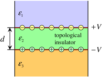
Coulomb interaction between electron and hole residing on opposite surfaces of TI film undergoes combined screening by three-dimensional dielectric environment and by two-dimensional electron and hole gases on these surfaces. We consider the three-layer dielectric system (Fig. 1), where is a dielectric permittivity of the TI film, and are dielectric permittivities of insulators above and below the film. In such system, the statically screened electron-hole interaction in the random phase approximation (RPA) is , where
| (1) |
(see also the similar formulas in LozovikYudson ; MacDonald ). Here
| (2) |
| (3) |
and are static polarizabilities of electron and hole gases on top and bottom surfaces of the film respectively, is the static anomalous interlayer polarizability; is the thickness of the film.
We shall consider the pairing in the static approximation, i.e. with neglecting frequency dependencies of a gap and pairing potential. At the static polarizability of Dirac electron or hole gas is Wunsch ; Hwang , where is the degeneracy factor, is the density of states at the Fermi level, is the Fermi momentum, is the Fermi velocity of Dirac electrons and holes ( for ZhangLiu ).
In this section we assume that the screening is the same as in intrinsic system without pairing, setting , . The main advantage of TI film over graphene bilayer is the smaller degeneracy factor (against for graphene) providing a weaker screening.
The static dielectric permittivity of strong three-dimensional TIs is rather large (e.g., for Bi2Se3 , for Bi2Te3 ), which looks disappointing for realization of the pairing. However when the thickness of the film is much smaller than the mean in-plane distance between electrons and holes (of the order of ), electric field lines responsible for electron-hole interaction pass mainly through the media above and below the film. In this case the screening is the same as in homogeneous medium with the dielectric permittivity and does not depend on the dielectric permittivity of the film itself (it follows directly from the limit of Eqs. (1)–(3) and was also noted in MacDonald ).
Generally, the pairing of massless Dirac fermions can be multi-band, when the both valence and conduction bands of both layers are affected by the pairing correlations. The multi-band theory of the pairing in graphene bilayer provided larger estimates for the gap and critical temperature than usual one-band BCS model both in static and dynamic approximations LozovikSokolik2 ; Mink ; LozovikOgarkov . For the sake of simplicity, here we shall consider the pairing in one-band BCS model, being aware, however, that our results for gap and critical temperature can be underestimated.
The integral BCS equation for the gap function in the one-band approximation is the following (analogously to that in LozovikSokolik1 ; LozovikSokolik2 ):
| (4) |
where and are azimuthal angles of the momenta and , entering the angular factor, specific to chiral Dirac electrons, is the Bogolyubov excitation energy, is the temperature.
According to the usual BCS recipe, we assume that the gap is nonzero and constant in some energy region of the half-width around the Fermi surface:
| (7) |
Using (4)–(7) we can find the gap at
| (8) |
and the critical temperature
| (9) |
Here is the Euler constant, is the dimensionless coupling constant calculated as an average of interaction potential times the density of states over the Fermi surface:
| (10) |
It is reasonable to take the pairing region half-width of the order of the chemical potential , since there are no other energy scales in the system (in contrast to superconductors, where can be taken of the order of Debye frequency). Thus hereafter we take . The maximal level of surface doping relative to the Dirac point in present three-dimensional TIs, being limited by a position of the bulk valence band, is about ZhangLiu . If we assume that the critical temperature (9) should be at least for the pairing to be observable, then at the maximal the coupling constant should be not smaller than .
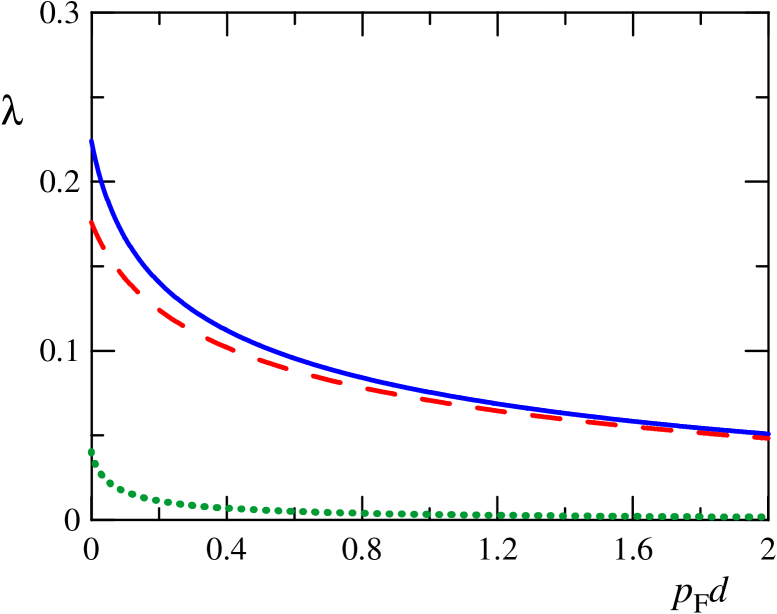
The coupling constants in the cases of suspended film with and of the film surrounded by a dielectric with are plotted in Fig. 3 at various . It is seen that in the both cases falls off very rapidly with increasing , and requires . We see also that strong screening by TI bilk significantly suppresses the coupling constant in the inverted structure “TI-insulator-TI” even in the most favorable case of the vacuum spacer with .
We can bring the coupling constant to its maximal value by approaching to zero and making the value of arbitrarily small. But the preexponential factor in (9), proportional to , also decreases in this case, thus we should not take too small in order to reach the highest . In Fig. 4 we plot in a suspended film with as a function of at different thicknesses . It is seen that is maximal at some nonzero dependent on . In order to keep above we should take the film thickness not exceeding . The similar conclusion was made in Mink1 . However in this case a tunneling between electron states on opposite surfaces of the film leads to significant hybridization of electron and hole states, which will be considered in the next section.
III Influence of hybridization
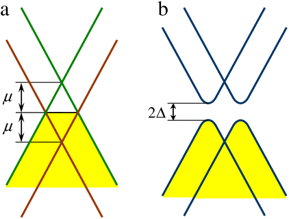
Wave functions of gapless electron states on a surface of strong three-dimensional TI decay exponentially in the bulk with characteristic depth of the order of several nanometers Lu ; Ebihara . In sufficiently thin films overlap of wave functions of the states belonging to opposite surfaces of the film can occur. This results in avoided crossing of dispersions of these states manifesting itself as opening of the hybridization gap . This gap in the spectrum is rather similar to the gap which could be opened by the pairing (see Fig. 2).
Indeed, the order parameter of the electron-hole pairing is , where is destruction operator for electron with momentum on the top surface and is destruction operator for hole with the opposite momentum on the bottom surface. Electron-hole transformation implies that , where is creation operator for electron with momentum on the bottom surface.
Therefore the pair of operators entering the order parameter = is analogous to that describing the process of momentum-conserving electron tunneling between top and bottom surfaces. Thus the gap equation for the total energy gap in the mean field approximation, describing both the pairing and hybridization, differs from (4) by the additional term in the right-hand side:
| (11) |
It is seen from (11) that the total gap becomes larger than hybridization gap due to the pairing. We shall solve Eq. (11), similarly to Eq. (4), in the BCS-like approximation (7).
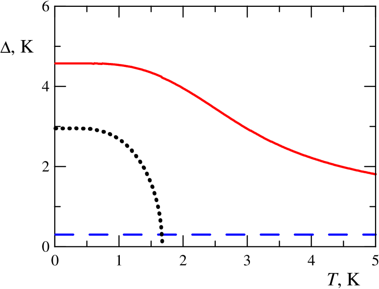
In Fig. 5 the example of solution of Eq. (11) is plotted under conditions when the hybridization gap is approximately 10 times smaller than the zero-temperature BCS gap calculated without hybridization. In the absence of hybridization, the gap would vanish at some critical temperature, but nonzero hybridization makes always nonzero and larger than . At the total gap is drastically increased even by weak hybridization — due to nonlinearity of Eq. (11) it is larger than just a sum ; at the gap gradually tends to . Thus the hybridization leads to the smearing of a phase transition into the paired state in close analogy with behavior of a ferromagnet in external magnetic field.
How can we observe the pairing in the presence of hybridization? Besides possible superfluid signatures of the pairing (see the Conclusions), we can still detect increase of the gap in the spectrum when the temperature is lowered — from the purely hybridization value at high temperatures to a somewhat larger value at zero (or very low) temperature (Fig. 5). To be observable, this increase should be relatively large, i.e. should not be very small in comparison with . In addition, the increase of the gap should occur in reasonably narrow temperature range. This range can be estimated by a characteristic temperature at which the gap is halfway between and , i.e. .
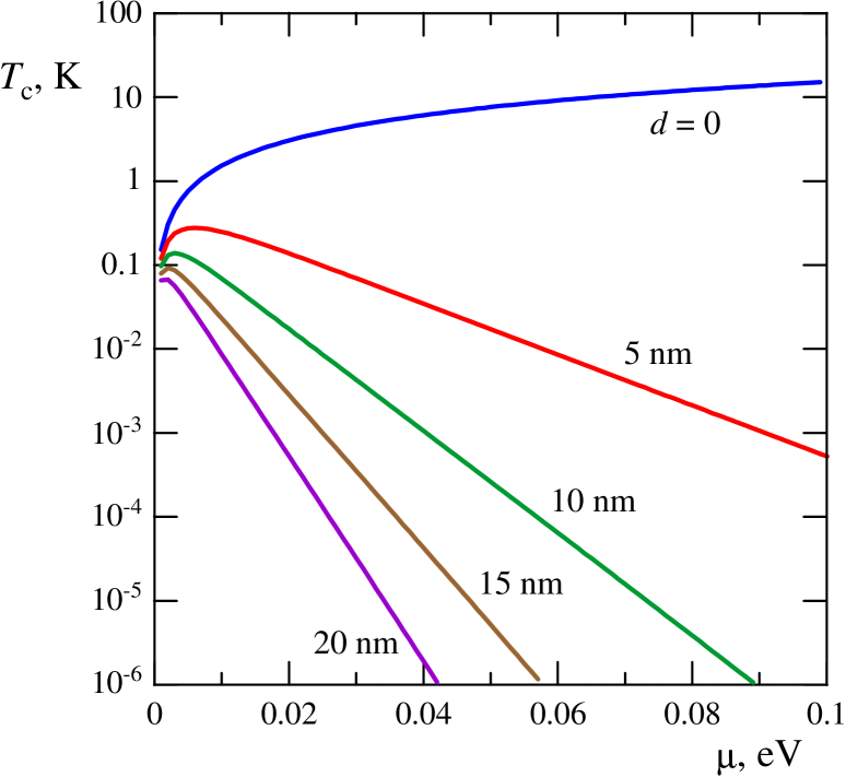
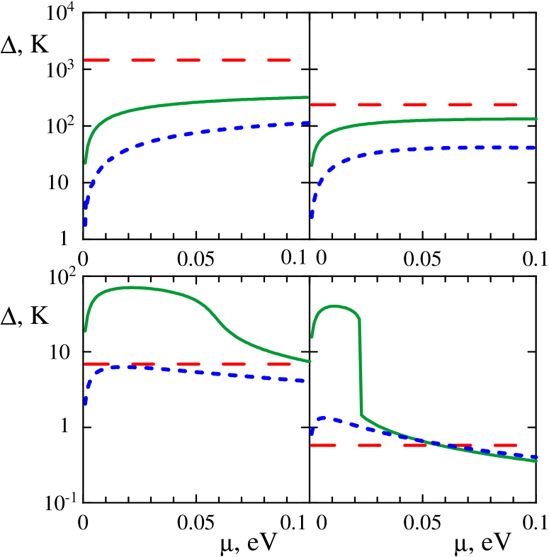
For calculations we take the data on hybridization gaps in films from the experiment Zhang , where the film thickness ranges from 2 to 5 QL, and from the theoretical paper Ebihara , where ranges from 1 to 16 QL (the close results for were also presented in the earlier paper Linder ). It should be noted that in the overlapping region of from 2 to 5 QL the experimental gaps from Zhang are several times larger than the calculated gaps from Ebihara , probably due to some impurities enhancing the interlayer tunneling.
According to these data, we take several examples of films with different and . We take at and at from Zhang as examples of large hybridization gaps (keeping in mind that the actual gap in the spectrum reported in the literature is ). As examples of small gaps, at and at are taken from Ebihara .
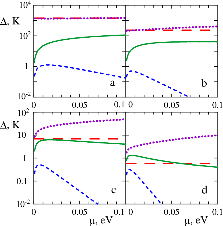
The aforementioned characteristics of the pairing with hybridization are shown in Fig. 6 for these four examples of films at . The gap calculated with hybridization is several orders of magnitude larger than the BCS gap. In the cases of strong hybridization at small (Fig. 6(a,b)), the increase of the total gap above the purely hybridization gap , being negligible compared with itself and occurring in a range of several thousands Kelvins, can hardly been observed. However when the hybridization is rather weak (Fig. 6(c,d)) the gap can grow significantly (up to several times) when we lower the temperature by several tens of Kelvins. In this case the gap itself is not larger than several Kelvins.
We can conclude that the temperature-dependent growth of the total gap is appreciable only if the hybridization is sufficiently weak, i.e. in moderately thin films. Since the gap itself becomes too small in thicker films, the optimal thickness for observing the pairing is about 5-8 QL.
IV Influence of disorder
As known, charged impurities suppress an electron-hole pairing in two-layer system LozovikYudson2 ; Bistritzer ; Efimkin since they, being usually uncorrelated in two layers, break the Cooper pairs by differently scattering two pair constituents. According to the Abrikosov-Gor’kov theory, applied to the case of electron-hole pairing, the Gor’kov equations remain the same as in the case of clean system, but with Matsubara frequencies and gaps at these frequencies renormalized in the following way:
| (12) |
where and are initial Mathubara frequencies and gap. The quantities correspond to intralayer ( and for top and bottom surfaces respectively) and interlayer () correlation functions of random impurity potential.
The gap equation (11) for disordered system takes the form:
| (13) |
When , the impurities do not affect the result of energy integration and frequency summation in (13) and thus the pairing characteristics remain the same. In superconductors it corresponds to the case of nonmagnetic impurities which, according to the Anderson theorem, do not suppress the pairing. In two-layer system this situation requires perfect anticorrelation of impurity potential between the layers and thus is hardly realizable in practice.
In reality, when a range of impurity potential significantly exceeds a film thickness (the limit ) and both surfaces of the film are equally disordered, we have , where is electron damping rate. For further calculations we consider the opposite case of short-range impurities and relatively thick films (), when , .
We can estimate on the basis of the data on surface carrier mobilities determining the surface conductivity of TI, expressed through the Drude formula:
| (14) |
where is the surface carrier concentration. In experiments on surface transport on (see the references cited on pp. 1088-1089 of the review Qi1 ) the measured mobilities vary from to . For calculations we choose the example of dirty sample where and the example of clean sample with .
In usual Abrikosov-Gor’kov theory, the pair-breaking disorder reduces both the gap and critical temperature, and sufficiently strong disorder can suppress the pairing completely. In our case the total gap is always larger than the hybridization gap . However in the presence of disorder their difference diminishes in comparison with that in clean system.
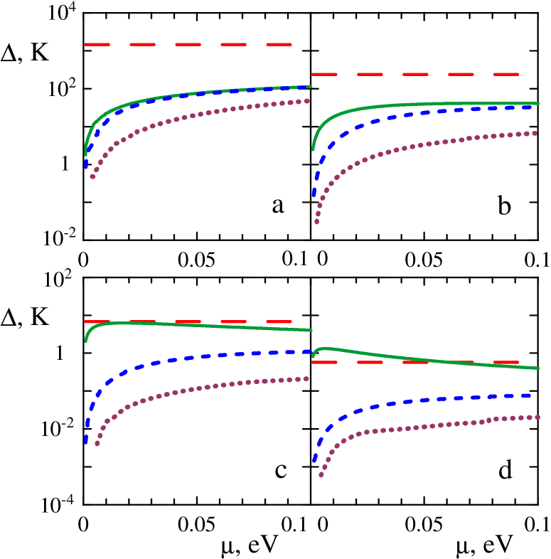
In Fig. 7 the increase of the gap calculated numerically from (12)–(13) is plotted at different disorder strengths for different examples of suspended films. It is seen that disorder rather weakly affects the pairing at strong hybridization (Fig. 7(a)) since the gap is very large in this case. At weak hybridization, when the effect of the pairing on the gap is expected to be most pronounced, even moderate disorder drastically reduces (Fig. 7(c,d)). Therefore we can conclude that the temperature-dependent increase of the gap due to the pairing can be observed only in very clean (with carrier mobilities ) and moderately thin (5-8 QL) TI films.
V Suppression of screening
In the previous sections we have considered the pairing potential screened by dielectric environment and by metallic electron and hole gases on two surfaces of the film. However this consideration is not completely self-consistent since the film becomes insulating on the surface due to appearance of the gap in the spectrum. When the gap is very large (especially in the case of strong hybridization) the screening by electron and hole gases can substantially differ from that in metallic system. In this case we should take into account self-consistent weakening of the screening caused by the pairing (the similar effect was considered earlier for semiconductor quantum wells LozovikBerman and graphene bilayer Sodemann ; LozovikRecent ).
When the gap appears in the system due to interlayer pairing or hybridization, the intralayer static polarizabilities and are no longer equal to the intrinsic polarizability and can be expressed in RPA as (see Sodemann ; LozovikRecent )
| (15) |
where , and are azimuthal angles of the momenta and , are indices denoting the conduction () and valence () bands (i.e. upper and lower parts of the double Dirac cone), is the energy of Bogolyubov excitation in the band . The coherence factors and are positive and determined by the equations:
| (16) |
In a two-layer system, interlayer pairing or hybridization also leads to appearance of the anomalous polarizability describing direct response of charge density in one layer on electric field in the other layer. In RPA it can be calculated as
| (17) |
We performed numerical solving of the gap equation (11) with taking into account hybridization and with the pairing potential (1)–(2) self-consistently screened by electrons and holes with the polarizabilities (15), (17). In this case the usual BCS method (7) which reduces the pairing potential to a single coupling constant is inapplicable since the integral in (10) diverges due to absence of long-range screening in the gapped system. Thus we perform full integration of (4) over momentum in the region where .
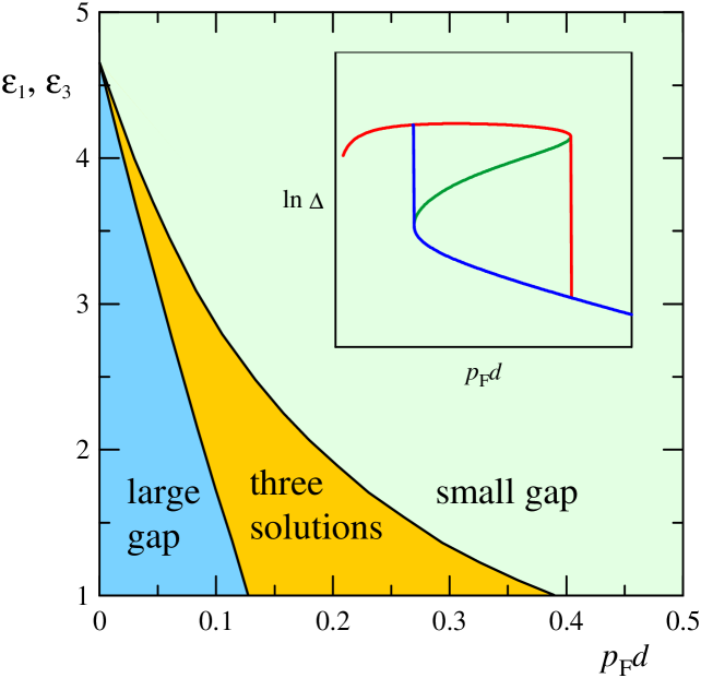
Our calculations show that at sufficiently weak coupling the gap is several times larger than in the case of metallic screening. At stronger coupling two additional solutions of the gap equation appear, which are by several orders of magnitude larger than the small gap that existed at weak coupling. Only the maximal of the resulting three gaps, providing the lowest ground state energy, will be established in the system. At further increase of the coupling (say, decrease of ) two smallest solutions disappear and only one large gap remains (see the inset in Fig. 8).
In Fig. 8 we show the phase diagram of film at with self-consistent weakening of the screening but without hybridization. At nonzero hybridization the regions of one large gap and of three solutions in this diagram would grow in size. At nonzero temperature the smallest gap gradually vanishes at small critical temperature (as in usual BCS model), but two largest gaps disappear at much larger temperature abruptly from nonzero values to zero, which is characteristic of the first-order phase transition (this fact was also noted in Sodemann ).
In Fig. 9 we demonstrate that becomes larger in several times at strong hybridization (Fig. 9(a,b)) and by the order of magnitude at weaker hybridization (Fig. 9(c,d)) in comparison with the results obtained with metallic screening. Our predictions for observability of the pairing become more optimistic, when we treat the screening self-consistently, especially for relatively thick films with weak hybridization, where even sharp transition to a strongly-correlated state can occur (Fig. 9(d)).
VI Conclusions
We have considered the pairing of spatially separated massless Dirac electrons and holes created on opposite surfaces of TI thin film by antisymmertic doping. The main advantage of such system over two-layer graphene system is four times smaller degeneracy of electron states leading to much weaker screening and much larger coupling constants. The effect of large bulk dielectric constant of the TI itself on the pairing can be negligible when the film is sufficiently thin.
Our calculations in BCS approximation show that the pairing gap is large enough to be observable when the film thickness is less than . In this case, however, tunneling between opposite surfaces leads to hybridization of electron and hole states. Such hybridization, on the one hand, effectively increases the gap. On the other hand, the pairing can become hardly observable on background of strong hybridization.
We show that the pairing causes increase of the total gap in the spectrum above the purely hybridization gap when the temperature is decreased. This effect can be observed only in moderately thin films (about 5-8 QL for ) where the hybridization is rather weak and effect of the pairing is noticeable on its background. Another way to observe the pairing can be based on measuring of change of the gap with varying surface electron and hole chemical potentials. Charged impurities and other disorder on surfaces of the film suppress the pairing, so as it can be observed only in sufficiently clean TIs (surface carrier mobility should be at least by the order of magnitude).
Also we have demonstrated that BCS approximation, by assuming the metallic screening by surface carriers, underestimates the coupling strength since the real screening in the gapped system is much weaker. The self-consistent treatment of the screening demonstrates that the gap can be by orders of magnitude larger than given by BCS model, and observation of the pairing in TI films can turn out to be more feasible. Multi-band and dynamical effects can additionally increase the gap.
Realization of electron-hole pairing in TI thin film is a difficult task including chemical doping of TI bulk to insulating state and, at the same time, doping of two opposite surfaces to electron- and hole-metallic states by means of gate electrodes or charged impurities. Another challenge is fabrication of separate contacts to the surfaces. However considerable progress achieved recently in experimental studies of TIs and TI thin films (see Hasan ; Qi1 and references therein) gives hope that conditions suitable for the electron-hole pairing can be reached in nearest years. In particular, transport measurements in a regime of coexistence of electrons and holes on opposite surfaces of film were carried out in Ref. Chen .
In this article, we considered only the manifestation of the pairing in the temperature dependence of the gap in the spectrum. For exciton condensate in electron-hole bilayers, such signatures as dipolar superfluidity LozovikYudson , Josephson-like effects LozovikYudson ; Shevchenko ; Klyuchnik ; Poushnov , peculiarities of the drag effect Conti ; Hu ; Mink1 and anomalous electromagnetic response Ovchinnikov ; Balatsky1 were predicted. Strong hybridization occurring in thin TI films imposes serious limitations on observability of these phenomena. As known, the tunneling in electron-hole bilayer leads to fixation of the condensate phase and to absence of uniform dipolar superfluidity. However the superfluidity can arise locally in a form of Josephson-like vortices Klyuchnik ; Poushnov or vortex lattice Shevchenko . In the latter case the dipolar current flowing along the bilayer should exceed some critical value in order for the vortex lattice to be stable. At high enough temperature the vortex lattice undergoes a dislocation-mediated melting when pairs of edge dislocations dissociate and proliferate (see Shevchenko ). It is interesting to note that dislocation ends in this case are topologically equivalent to vortices in a superfluid condensate and thus can settle Majorana zero energy modes Seradjeh1 which can be manipulated for the purpose of quantum computations.
The work was supported by Russian Foundation for Basic Research. D.K.E. and A.A.S. were also supported by the Dynasty Foundation and by the grant of the President of Russian Federation MK-5288.2011.2.
References
- (1) M.Z. Hasan, C.L. Kane, Rev. Mod. Phys. 82, 3045 (2010).
- (2) X.-L. Qi, S.-C. Zhang, Rev. Mod. Phys. 83, 1057 (2011).
- (3) H. Zhang, C.-X. Liu, X.-L. Qi, X. Dai, Z. Fang, S.-C. Zhang, Nature Phys. 5, 438 (2009).
- (4) D. Hsieh, Y. Xia, L. Wray, D. Qian, A. Pal, J.H. Dil, J. Osterwalder, F. Meier, G. Bihlmayer, C.L. Kane, Y.S. Hor, R.J. Cava, M.Z. Hasan, Science 323, 919 (2009).
- (5) Y.L. Chen, J.G. Analytis, Z.H. Chu, Z.K. Liu, S.K. Mo, X.L. Qi, H.J. Zhang, D.H. Lu, X. Dai, Z. Fang, S.C. Zhang, I.R. Fisher, Z. Hussain, Z.X. Shen, Science 325, 178 (2009).
- (6) Y. Xia, L. Wray, D. Qian, D. Hsieh, A. Pal, H. Lin, A. Bansil, D. Grauer, Y. Hor, R. Cava, M.Z. Hasan, Nature Phys. 5, 398 (2009).
- (7) A.H. Castro Neto, F. Guinea, N.M.R. Peres, K.S. Novoselov, A.K. Geim, Rev. Mod. Phys. 81, 109 (2009).
- (8) Q. Liu, C.-X. Liu, C. Xu, X.-L. Qi, S.-C. Zhang, Phys. Rev. Lett. 102, 156603 (2009).
- (9) Y.L. Chen, J.-H. Chu, J.G. Analytis, Z.K. Liu, K. Igarashi, H.-H. Kuo, X.L. Qi, S.K. Mo, R.G. Moore, D.H. Lu, M. Hashimoto, T. Sasagawa, S.C. Zhang, I.R. Fisher, Z. Hussain, Z.X. Shen, Science 329, 659 (2010).
- (10) X.L. Qi, T.L. Hughes, S.C. Zhang, Phys. Rev. B 78, 195424 (2008).
- (11) A.M. Essin, J.E. Moore, D. Vanderbilt, Phys. Rev. Lett. 102, 146805 (2009).
- (12) L. Fu, C.L. Kane, Phys. Rev. Lett. 100, 096407 (2008).
- (13) Y.S. Hor, A.J. Williams, J.G. Checkelsky, P. Roushan, J. Seo, Q. Xu, H.W. Zandbergen, A. Yazdani, N.P. Ong, R.J. Cava, Phys. Rev. Lett. 104, 057001 (2010).
- (14) C.-K. Lu, I.F. Herbut, Phys. Rev. B 82, 144505 (2010).
- (15) M.C. Diamantini, P. Sodano, C.A. Trugenberger, New J. Phys. 14, 063013 (2012).
- (16) G. Zhang, H. Qin, J. Teng, J. Guo, Q. Guo, X. Dai, Z. Fang, K. Wu, Appl. Phys. Lett. 95, 053114 (2009).
- (17) H.D. Li, Z.Y. Wang, X. Kan, X. Guo, H.T. He, Z. Wang, J.N. Wang, T.L. Wong, N. Wang, M.H. Xie, New J. Phys. 12, 103038 (2010).
- (18) Y.-Y. Li, G. Wang, X.-G. Zhu, M.-H. Liu, C. Ye, X. Chen, Y.-Y. Wang, K. He, L.-L. Wang, X.-C. Ma, H.-J. Zhang, X. Dai, Z. Fang, X.-C. Xie, Y. Liu, X.-L. Qi, J.-F. Jia, S.-C. Zhang, Q.-K. Xue, Adv. Mater. 22, 4002 (2010).
- (19) N. Bansal, Y.S. Kim, E. Edrey, M. Brahlek, Y. Horibe, K. Iida, M. Tanimura, G.-H. Li, T. Feng, H.-D. Lee, T. Gustafsson, E. Andrei, S. Oh, Thin Solid Films 520, 224 (2010).
- (20) D. Kong, W. Dang, J.J. Cha, H. Li, S. Meister, H. Peng, Z. Liu, Y. Cui, Nano Lett. 10, 2245 (2010).
- (21) S.S. Hong, W. Kundhikanjana, J.J. Cha, K. Lai, D. Kong, S. Meister, M.A. Kelly, Z.-X. Shen, Y. Cui, Nano Lett. 10, 3118 (2010).
- (22) K.M.F. Shahil, M.Z. Hossain, D. Teweldebrhan, A.A. Balandin, Appl. Phys. Lett. 96, 153103 (2010).
- (23) D. Teweldebrhan, V. Goyal, A.A. Balandin, Nano Lett. 10, 1209 (2010).
- (24) J. Linder, T. Yokoyama, A. Sudbo, Phys. Rev. B 80, 205401 (2009).
- (25) Y. Zhang, K. He, C.-Z. Chang, C.-L. Song, L.-L. Wang, X. Chen, J.-F. Jia, Z. Fang, X. Dai, W.-Y. Shan, S.-Q. Shen, Q. Niu, X.-L. Qi, S.-C. Zhang, X.-C. Ma, Q.-K. Xue, Nature Phys. 6, 584 (2010).
- (26) Y. Sakamoto, T. Hirahara, H. Miyazaki, S.I. Kimura, S. Hasegawa, Phys. Rev. B 81, 165432 (2010).
- (27) G. Wang, X. Zhu, J. Wen, X. Chen, K. He, L. Wang, X. Ma, Y. Liu, X. Dai, Z. Fang, J. Jia, Q. Xue, Nano Research 3, 874 (2010).
- (28) K. Park, J.J. Heremans, V.W. Scarola, D. Minic, Phys. Rev. Lett. 105, 186801 (2010).
- (29) K. Ebihara, K. Yada, A. Yamakage, Y. Tanaka, Physica E 44, 885 (2012).
- (30) H.-Z. Lu, W.-Y. Shan, W. Yao, Q. Niu, S.-Q. Shen, Phys. Rev. B 81, 115407 (2010).
- (31) X. Zhang, J. Wang, S.-C. Zhang, Phys. Rev. B 82, 245107 (2010).
- (32) Z. Yang, J.H. Han, Phys. Rev. B 83, 045415 (2011).
- (33) A.A. Zyuzin, A.A. Burkov, Phys. Rev. B 83, 195413 (2011).
- (34) B. Seradjeh, J.E. Moore, M. Franz, Phys. Rev. Lett. 103, 066402 (2009).
- (35) N. Hao, P. Zhang, Y. Wang, Phys. Rev. B 84, 155447 (2011).
- (36) G.Y. Cho, J.E. Moore, Phys. Rev. B 84, 165101 (2011).
- (37) D. Tilahun, B. Lee, E.M. Hankiewicz, A.H. MacDonald, Phys. Rev. Lett. 107, 246401 (2011).
- (38) Z. Wang, N. Hao, Z.-G. Fu, P. Zhang, New J. Phys. 14, 063010 (2012).
- (39) M.P. Mink, H.T.C. Stoof, R.A. Duine, M. Polini, G. Vignale, Phys. Rev. Lett. 108, 186402 (2012).
- (40) E.G. Moon, C. Xu, Europhys. Lett. 97, 66008 (2012).
- (41) I. Sodemann, D.A. Pesin, A.H. MacDonald, Phys. Rev. B 85, 195136 (2012).
- (42) B. Seradjeh, ArXiv:cond-mat/1203.6628.
- (43) Y. Kim, E.M. Hankiewicz, M.J. Gilbert, ArXiv:cond-mat/1204.6351.
- (44) B. Seradjeh, Phys. Rev. B 85, 235146 (2012).
- (45) Yu.E. Lozovik, V.I. Yudson, Pisma v ZhETF 22, 556 (1975) [JETP Lett. 22, 274 (1975)]; Zh. Eksp. Teor. Fiz. 71, 738 (1976) [Sov. Phys. JETP 44, 389 (1976)].
- (46) Yu.E. Lozovik, V.I. Yudson, Solid State Commun. 21, 211 (1977).
- (47) Yu.E. Lozovik, O.L. Berman, Zh. Eksp. Teor. Fiz. 111, 1879 (1997) [JETP 84, 1027 (1997)].
- (48) S.I. Shevchenko, Phys. Rev. Lett. 72, 3242 (1994).
- (49) Yu.E. Lozovik, A.A. Sokolik, Pis ma v ZhETF 87, 61 (2008) [JETP Lett. 87, 55 (2008)].
- (50) H. Min, R. Bistritzer, J.-J. Su, A.H. MacDonald, Phys. Rev. B 78, 121401(R) (2008).
- (51) C.-H. Zhang, Y.N. Joglekar, Phys. Rev. B 77, 233405 (2008).
- (52) R. Bistritzer, A.H. MacDonald, Phys. Rev. Lett. 101, 256406 (2008).
- (53) M.Yu. Kharitonov, K.B. Efetov, Phys. Rev. B 78, 241401(R) (2008); Semicond. Sci. Tech. 25, 034004 (2010).
- (54) Yu.E. Lozovik, A.A. Sokolik, Phys. Lett. A 374, 326 (2009); Eur. Phys. J. B 73, 195 (2009).
- (55) Yu.E. Lozovik, S.L. Ogarkov, A.A. Sokolik, Philos. Trans. Roy. Soc. A 368, 5417 (2010).
- (56) M.P. Mink, H.T.C. Stoof, R.A. Duine, A.H. MacDonald, Phys. Rev. B 84, 155409 (2011).
- (57) D.K. Efimkin, V.A. Kulbachinskii, Yu.E. Lozovik, Pis ma v ZhETF 93, 238 (2011) [JETP Lett. 93, 219 (2011)].
- (58) Yu.E. Lozovik, S.L. Ogarkov, A.A. Sokolik, ArXiv:cond-mat/1202.4978v2.
- (59) B. Wunsch, T. Stauber, F. Sols, F. Guinea, New J. Phys. 8, 318 (2006).
- (60) E.H. Hwang, S. Das Sarma, Phys. Rev. B 75, 205418 (2007).
-
(61)
Collaboration: Authors and editors of the volumes III/17E-17F-41C: Bismuth selenide (Bi2Se3) optical properties,
dielectric constants. Madelung, O., Rossler, U., Schulz, M. (ed.). SpringerMaterials — The Landolt-Bornstein Database
(http://www.springermaterials.com).
DOI: 10.1007/10681727_945 -
(62)
Collaboration: Authors and editors of the volumes III/17E-17F-41C: Bismuth telluride (Bi2Te3) optical properties,
dielectric constant. Madelung, O., Rossler, U., Schulz, M. (ed.). SpringerMaterials — The Landolt-Bornstein Database
(http://www.springermaterials.com).
DOI: 10.1007/10681727_963 - (63) A.V. Klyuchnik, Yu.E. Lozovik, Zh. Eksp. Teor. Fiz. 76, 670 (1978) [Sov. Phys. JETP 49, 335 (1978)].
- (64) J. Chen, X.Y. He, K.H. Wu, Z.Q. Ji, L. Lu, J.R. Shi, J.H. Smet, Y.Q. Li, Phys. Rev. B 83, 241304(R) (2011).
- (65) Yu.E. Lozovik, A.V. Poushnov, Phys. Lett. A 228, 399 (1997).
- (66) S. Conti, G. Vignale, A.H. MacDonald, Phys. Rev. B 57, R6846 (1998).
- (67) B.Y.-K. Hu, Phys. Rev. Lett. 85, 820 (2000).
- (68) Yu.E. Lozovik, I.V. Ovchinnikov, Phys. Rev. B 66, 075124 (2002).
- (69) A.V. Balatsky, Y.N. Joglekar, P.B. Littlewood, Phys. Rev. Lett. 93, 266801 (2004).