Manifestation of chiral tunneling at a tilted graphene junction
Abstract
Electrons in graphene follow unconventional trajectories at PN junctions, driven by their pseudospintronic degree of freedom. Significant is the prominent angular dependence of transmission, capturing the chiral nature of the electrons and culminating in unit transmission at normal incidence (Klein tunneling). We theoretically show that such chiral tunneling can be directly observed from the junction resistance of a tilted interface probed with separate split gates. The junction resistance is shown to increase with tilt in agreement with recent experimental evidence. The tilt dependence arises because of the misalignment between modal density and the anisotropic transmission lobe oriented perpendicular to the tilt. A critical determinant is the presence of edge scattering events that can completely reverse the angle-dependence. The absence of such reversals in the experiments indicates that these edge effects are not overwhelmingly deleterious, making the premise of transport governed by electron ‘optics’ in graphene an exciting possibility.
pacs:
72.80.Vp, 73.63.-b, 72.10.-dA striking feature of electron flow in graphene, gated uniformly or electrostatically ‘doped’ into junctions, is the non-trivial dynamics of its pseudospins arising from its orthogonal dimer basis sets. The overall photon like dispersion propels electrons along trajectories intuitive of Snell’s law, conserving quasi-momentum components transverse to the interface. However, the corresponding ‘Fresnel equations’ are qualitatively different from their optical counterpart, determined by conservation of pseudospins. In particular, graphene electrons are chiral in nature meaning the pseudospin components are related to the direction of momentum. This results in perfect transmission at normal incidence Katsnelson et al. (2006) regardless of voltage gradients across the junction (Klein tunneling). For other incident angles, the spinor mismatch leads to a unique angle dependent transmission across the junction. Thus, while conventional electronics in graphene faces possibly steep challenges Schwierz (2010), the dynamics of pseudospintronics can usher in novel concepts such as electronic Veselago lens Cheianov et al. (2007), subthermal switches driven by geometry induced metal-insulator transition Sajjad and Ghosh (2011) and Andreev reflections Beenakker (2006).
Despite the exciting physics of chiral electron flow, its measurable signatures have so far been sparse and indirect. Signatures of Klein tunneling were seen Gorbachev et al. (2008); Stander et al. (2009) in the preferential transmission of normally incident carriers predicted in Cheianov and Fal’ko (2006). A more direct measurement was the conductance oscillation in an structure Young and Kim (2009). The reflection amplitude undergoes a phase shift of at normal incidence under the action of a magnetic field, due to the cyclotron bending of the carriers Shytov et al. (2008). However, the main underlying physics of the angle dependent electron transmission has not been explicitly measured. Neither has there been a proper model that can capture both the quantum mismatch of spinors over the entire doping regime, as well as diffusive scattering to explore their robustness to impurity and edge scattering events.
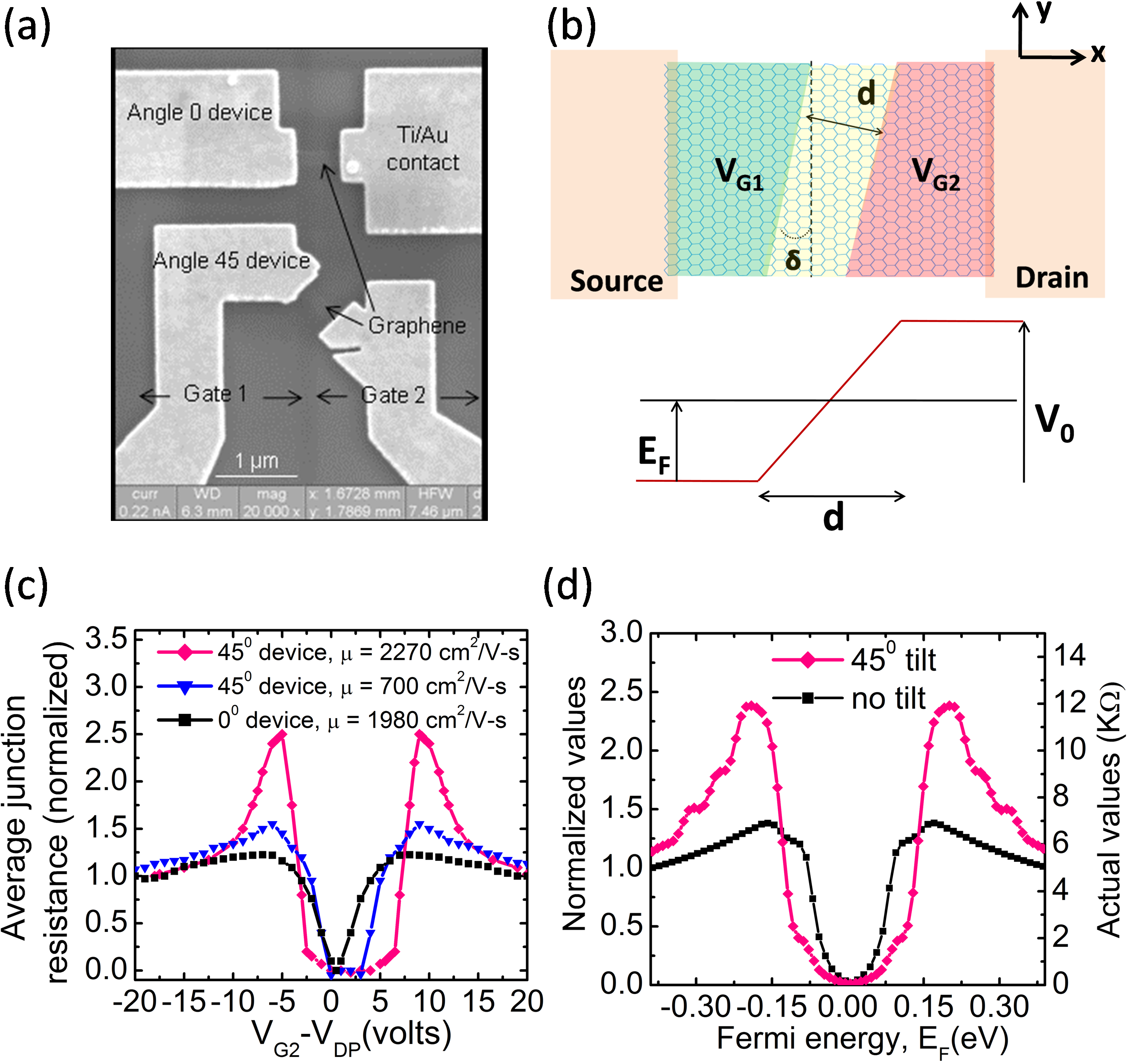
In this paper we focus on a tilted GPNJ (i) to show that it serves as an explicit signature of chiral tunneling. We show that the junction resistance (similar to the odd resistance shown in other experiments Gorbachev et al. (2008); Stander et al. (2009)) is higher than the non-tilted device (Fig. 1). We argue that this enhancement originates from the chiral nature of graphene electrons which manifests itself through the highly angle dependent transmission characteristics of GPNJ (Fig. 2). The angular transmission lobe, oriented perpendicular to the interface is rotated with the tilt, where fewer transmitting modes exist. Therefore the conductance modulation would not happen for non-chiral, non-relativistic electrons with isotropic transmission. The results follow closely with our recent transport measurements of a tilted GPNJ in a structure that has separately controlled split-gate voltages Sutar et al. (2011, 2012). (ii) We present an
exact analytical solution to the spinor mismatch problem as well as non-equilibrium Green’s function (NEGF) based atomistic numerical calculation. An efficient matrix inversion algorithm is employed to reach near experimental dimensions and capture both quantum mechanical and diffusive contributions to the overall resistance.
We find that charged impurity scattering dilutes, but does not eliminate the modulation in conductance (Figs. 1, 3). (iii) Notably, we demonstrate that multiple scattering events at edges can reverse the trend in modulation, giving an interfacial resistance that decreases with tilt (Fig. 4). Such decrease has been seen in the past Low and Appenzeller (2009), but their physical origin has not been identified so far. The absence of such a reversal in experiments surprisingly points to their elimination, possibly through incoherent scattering processes dominant at the strained edges.
Analytical model. The conductance of a GPNJ can be written as, where is the conductance quantum including spin and valley degeneracies and is the incident angle dependent transmission probability with . is the number of modes from the incident side for a given Fermi energy relative to its Dirac point and can be approximated as over the linear E-k regime.
The angle dependent transmission is obtained by pseudospin conservation across the junction Sajjad and Ghosh (2011)
This is a general form of the transmission expression in Low et al. (2009); Cheianov and Fal’ko (2006) and works for the entire voltage range from to junction. The incident and refracted angles and are related by Snell’s law Cheianov et al. (2007), , with (Fig. 1) being the voltage barrier across the junction, and . The Snell’s law arises from transverse quasi-momentum conservation (energy band diagram in Fig. 1(b)). For the rest of the paper, we use the average transmission of all modes, .
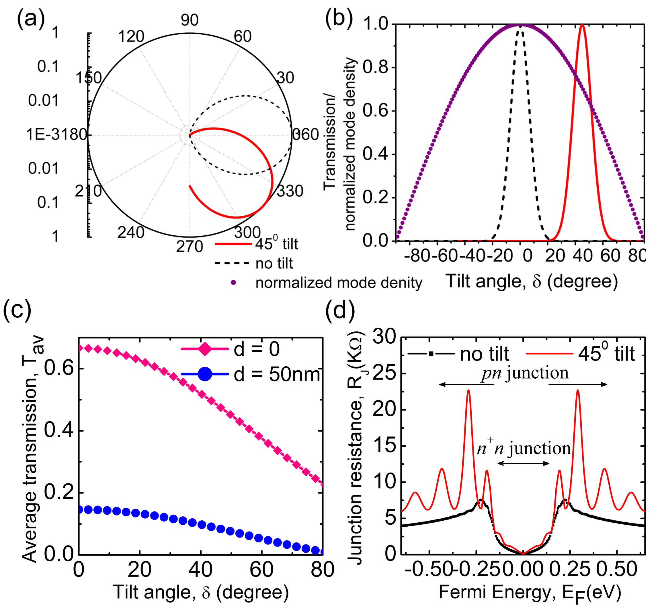
For a tilted junction, the incoming mode angles are modified, so that the conductance becomes,
| (2) |
where is the tilt angle as shown in Fig. 1. In Eq. 2 the effective split between the two gates is . As a result of the angle dependence, the transmission lobe at a particular energy will rotate by the tilt angle (Fig. 2a). The transverse wavevector gives , so that the mode density decreases as we go to higher angles relative to the transport axis. A tilt at the junction thus shifts the transmission window onto a high angle region where the mode density is less, decreasing the overall transmission (Fig. 2c). In the limit when the no. of modes is very few, the experiment will give the mode resolved angle dependent transmission properties (Fig. 2(a)). For an abrupt, symmetric junction, the transmission expression reduces to from Eq. Manifestation of chiral tunneling at a tilted graphene junction and it is easy to see the impact of tilt,
| (3) |
The factor arises from the wavefunction mismatch across the junction and the tilt introduces an additional scaling factor, which further reduces conductance. The gradual decrease of with in Fig. 2(c) constitutes a direct manifestation of chiral tunneling in graphene.
To connect with experimental measurements, we next analyze the variation of the junction resistance in presence of an intrinsic background doping () in the graphene sheet (Fig. 2d). We vary the gate voltages so that but a nonzero makes it an asymmetric GPNJ. The effective gate voltages on the graphene sheet are and , where is the capacitive gate transfer factor. The junction resistance can be written as Datta (1997),
| (4) |
Fig. 2(d) plots against , the amount of shift in the Dirac point by , for a 100nm wide graphene sheet with a split gate separation . For the voltage range , we are in the regime for positive and for negative. Under these near homogeneous conditions, the junction resistance predicted by Eqs. 1-4 is small, because the pseudospin states match and there is no WKB tunneling term in Eq. Manifestation of chiral tunneling at a tilted graphene junction. When , we are in the junction regime and resistance jumps to a high value, primarily due to the WKB factor in Eq. Manifestation of chiral tunneling at a tilted graphene junction (similar trend was seen in Gorbachev et al. (2008); Stander et al. (2009)). The rate of change in with is determined by . For the tilted junction, the junction resistance is higher than the non-tilted resistance. We see oscillation in the resistance (Fig. 2(d)) for the single junction. This is different from the interference oscillation in Ref. Young and Kim (2009) for the resonant cavity formed in strucure. This can be understood from the conductance in the junction regime, simplified as for large . With increasing gate voltage (higher ) we have more modes () in the summation with each mode transmitting with exponentially reduced magnitude. The two opposing effects generate a sequence of peaks and valleys and dominate when we sum over a few modes (either with quantization or tilt) at low temperature.
Numerical model. An atomistic, numerical calculation of the junction resistance is shown in Fig. 1 (d) at 80K temperature. We use NEGF formalism for a 100nm wide graphene sheet with , close to experimental dimensions (width 200-300nm). A single orbital basis for each carbon atom is used to compute the Hamiltonian , while the contact self-energies are calculated using a recursive technique. The retarded Green’s functions are calculated as using the algorithm in Svizhenko et al. (2002), is the electrostatic potential inside the device. In units of , the conductance is calculated as , where the contact broadening functions are the anti-Hermitian components of . For ballistic transport, equals , the number of modes for a uniformly gated sheet, and for a junction. Combining these two, we calculate and from Eq. 4, which shows a jump with tilt in the junction regime, very similar to the experiment.
Charged impurity scattering dilutes tilt dependence. The experimental device is on a SiO2 substrate and the transport is diffusive with a mobility varying from 700-3000 cm2/V-s. It is natural to inquire how the theoretical model, which so far had no scattering, corresponds to experiments. To explore this feature, we included the impact of charged impurity scattering in our model. We use a sequence of screened Gaussian potential profiles for
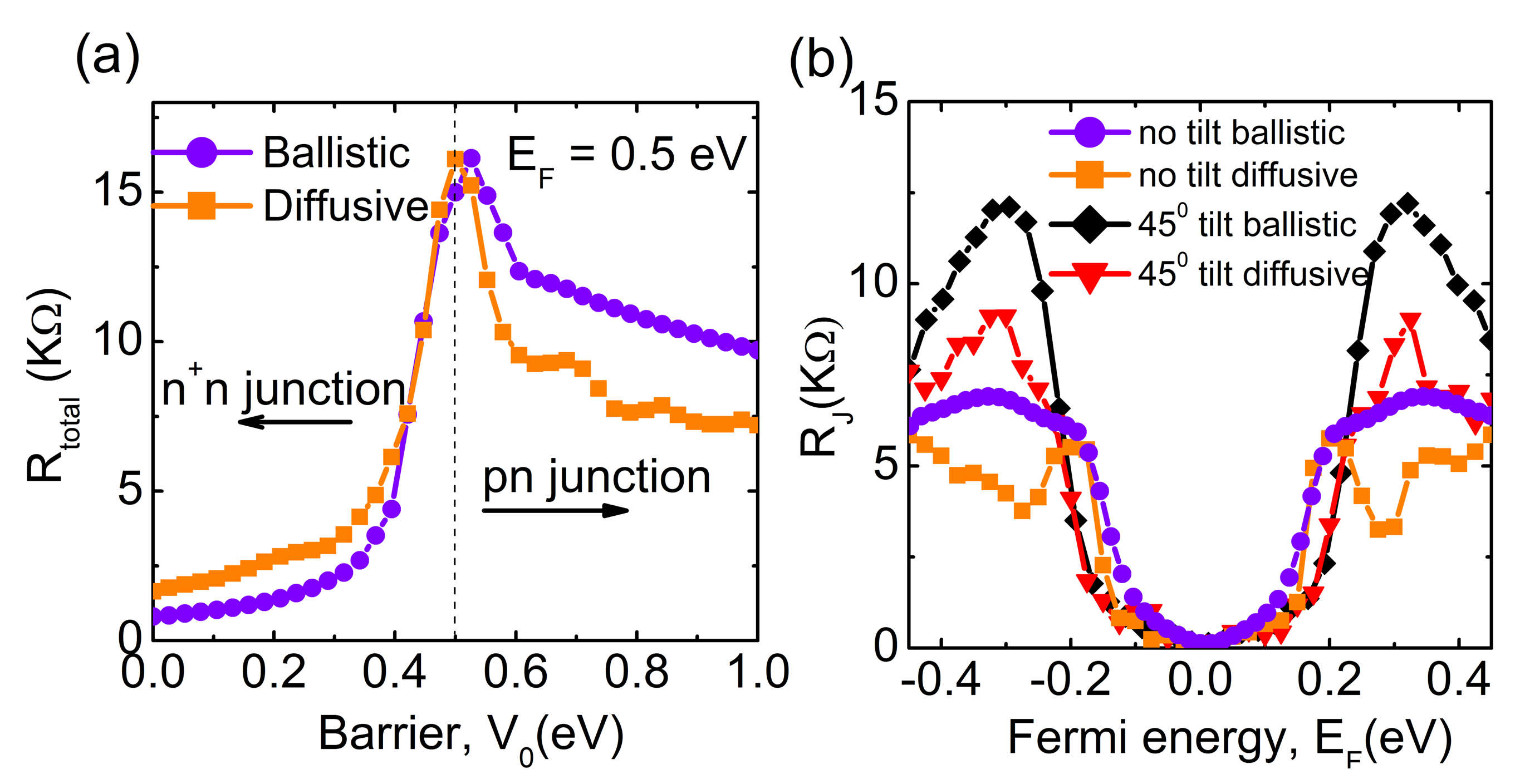
the impurity scattering centers Kłos and Zozoulenko (2010); Peres (2010); Lewenkopf et al. (2008), , that specifies the strength of the impurity potential at atomic site r, with being the positions of the impurity atoms and the screening length ( 8 times the C-C bond for long range scatterers). The amplitudes lie in the range ( 0.5 times the C-C coupling parameter) and is the impurity concentration ( 5 x 1011 cm-2). Note that the purely diffusive model discussed in Fogler et al. (2008); Stander et al. (2009); Gorbachev et al. (2008) ignores the quantum mechanical spinor mismatch and WKB scaling and therefore underestimates the junction resistance for cleaner samples. Our NEGF based numerical model on the other hand captures both the quantum mechanical and impurity limited resistance contributions simulataneously. The junction resistance is now calculated by eliminating the contact and device resistance Sutar et al. (2012)
| (5) |
where the first two terms contain the junction resistance, while the last two don’t.
Fig. 3(a) shows the impact of the impurity scatterings on the total resistance and 3(b) on the junction resistance. We take the average resistance over many impurity configurations. This puts a constraint on the computation size, so we show calculations this time for a smaller device (50nm wide). We find that both tilted and non-tilted junction resistances are suppressed, thereby retaining the difference between the two. This reduction in junction resistance with scattering is quite consistent with the experiment (Fig. 1(c), red line is for a device with mobility 2270cm2/V-s, while the blue triangle is for with lower mobility, 700cm2/V-s).
The reduction in the junction resistance from ballistic to diffusive transport can be understood from the trend in total resistance, shown in Fig. 3(a). Now we keep fixed and vary so that we go from to junction. We see a clear asymmetry in the R-VG Low et al. (2009); Stander et al. (2009) (purple line normalized to the orange line in Fig. 3(a) for comparison). The asymmetry confirms the presence of junction, which reduces the conductance due to spinor mismatch. The presence of impurity scattering reduces this asymmetry while increasing the overall resistance (red line). The impurity potentials create a random potential variation throughout the graphene sheet on top of the applied gate voltages, thus blurring the presence of a junction. Therefore the resistance due to spinor mismatch becomes less noticeable (Fig. 3(b)). Indeed, the experimental data of the total resistance indicates an increase in asymmetry in the tilted junction Sutar et al. (2012), signifying an increase in the junction resistance.
Edge scattering can reverse tilt dependence. A striking feature on the experimental results is their agreement with Eq. 3. This match is remarkable, considering that the equation was derived assuming no edge reflections and the fact that past numerical study Low and Appenzeller (2009) showed in fact an increase in conductance with tilt. We argue that the above reversal of junction conductance with tilt is entirely due to edge scattering events. Indeed, from an atomistic NEGF calculation with shorter widths than lengths, we find that the transmission now shows a pronounced local maximum (Fig. 4(a) orange line) in agreement with Low and Appenzeller (2009), increasing thereby the junction resistance.
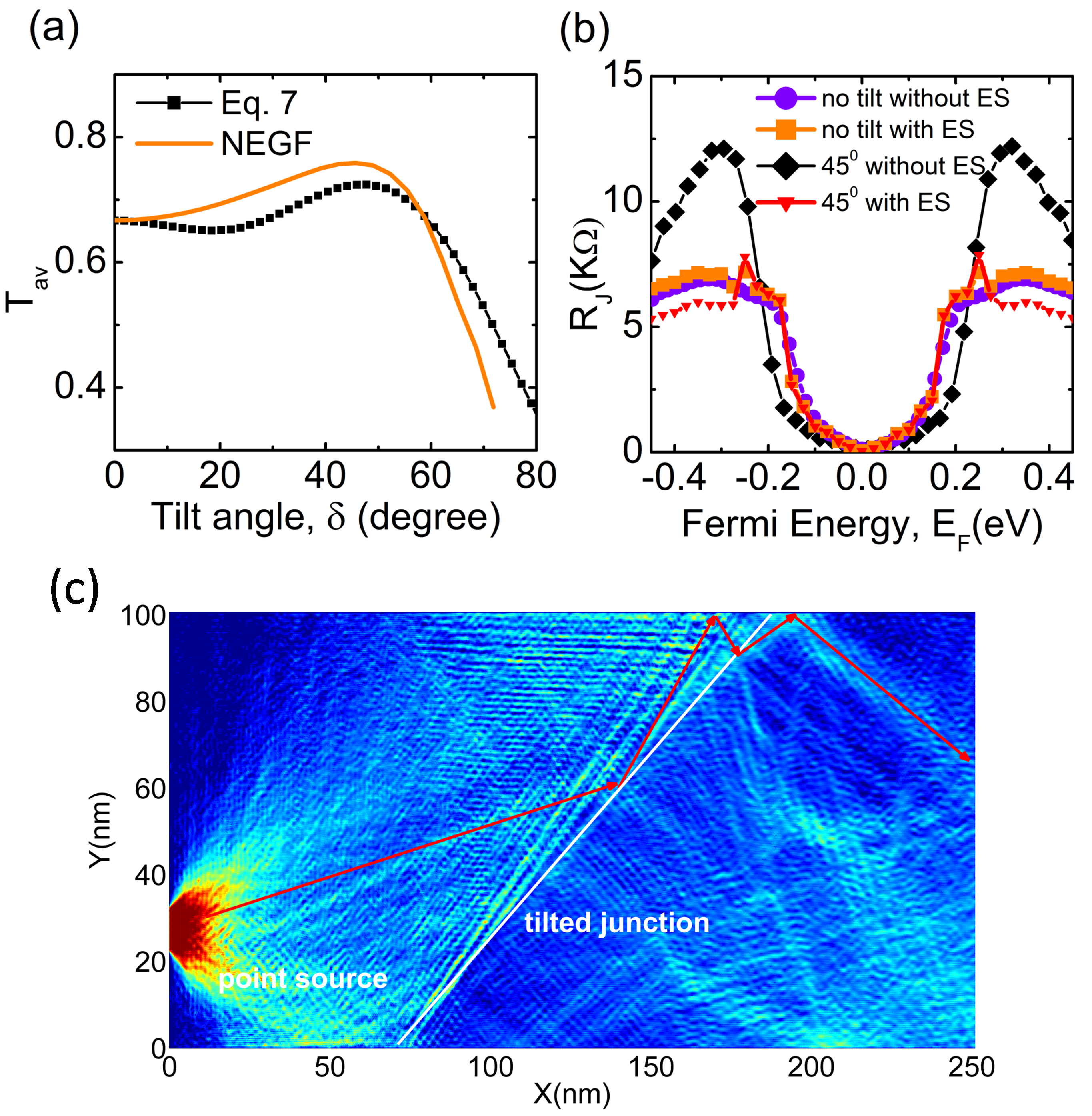
We summarize this in Fig. 4(b), where an increasing tilt makes the resistance increase for the short channel 125nm x 50nm device (a transition from purple circle to black diamond), but decrease for the longer 200nm x 50nm device (orange square to red triangle). Bearing in mind that the gate split is 100nm, the short channel device significantly reduces edge scatterings.
To better understand the origin of such a resistance reversal, we inject electrons with a small contact at the left edge (bright red spot in Fig. 4c) and plot the spatial current density under a small drain bias. The numerically computed electron trajectories show how a tilt can enhance forward scattering events at the edge and thus an increase in conductance. The enhancement arises from simple ‘geometrical optics’ dictated by Snell’s law. We can identify the incident wide angle modes (), for which the reflected ‘ray’ hits the upper edge with a positive directed velocity. Such a mode will reflect back towards the junction again. The contribution from the positively directed edge scattering event is given by
Note that only the incident angles below the critical angle are considered while setting the limits of the integration.
With the added contribution from edge scattering, the net mode-averaged transmission is given by
| (7) |
where the s are extracted from the corresponding ratios and is a parameter that describes the efficiency of edge scattering. In the absence of edge scattering (), and decreases with tilt (Fig. 2c). However in the presence of strong edge scattering (), the added forward edge scattering term in Eq. 7 closely reproduces the NEGF result with the local transmission maximum (Fig. 4a, black dotted line). Comparing these results with experiments indicates that such edge scattering events are clearly minor. We conjecture that the coherent forward scattering processes captured by NEGF can be diluted down in the experiments by the presence of incoherent scattering processes arising at the strained and rough edges of the graphene samples that tend to dephase or perhaps even trap the electrons.
The experimental observation of chiral tunneling, particularly in the face of impurity and edge scattering, opens up the possibility of graphene’s ‘geometric optics’ based applications, e.g. lens, switches and wave-guides. Analogous results are expected in bilayer graphene, but not in achiral materials like 2-D hexagonal boron nitride.
The authors acknowledge funding support from INDEX-NRI and useful discussions with T. Low.
References
- Katsnelson et al. (2006) M. I. Katsnelson, K. S. Novoselov, and A. K. Geim, Nat Phys 2, 620 (2006).
- Schwierz (2010) F. Schwierz, Nat Nano 5, 487 (2010).
- Cheianov et al. (2007) V. V. Cheianov, V. Fal’ko, and B. L. Altshuler, Science 315, 1252 (2007).
- Sajjad and Ghosh (2011) R. N. Sajjad and A. W. Ghosh, Appl. Phys. Lett. 99, 123101 (2011).
- Beenakker (2006) C. W. J. Beenakker, Phys. Rev. Lett. 97, 067007 (2006).
- Gorbachev et al. (2008) R. V. Gorbachev, A. S. Mayorov, A. K. Savchenko, D. W. Horsell, and F. Guinea, Nano Letters 8, 1995 (2008).
- Stander et al. (2009) N. Stander, B. Huard, and D. Goldhaber-Gordon, Phys. Rev. Lett. 102, 026807 (2009).
- Cheianov and Fal’ko (2006) V. V. Cheianov and V. I. Fal’ko, Phys. Rev. B 74, 041403 (2006).
- Young and Kim (2009) A. F. Young and P. Kim, Nat Phys 5, 222 (2009).
- Shytov et al. (2008) A. V. Shytov, M. S. Rudner, and L. S. Levitov, Phys. Rev. Lett. 101, 156804 (2008).
- Sutar et al. (2011) S. Sutar, E. Comfort, and J. U. Lee, International Semiconductor Device Research Symposium (ISDRS) , 1 (2011).
- Sutar et al. (2012) S. Sutar, E. S. Comfort, Liu, J., T. Taniguchi, K. Watanabe, and J. U. Lee, unpublished (2012).
- Low and Appenzeller (2009) T. Low and J. Appenzeller, Phys. Rev. B 80, 155406 (2009).
- Low et al. (2009) T. Low, S. Hong, J. Appenzeller, S. Datta, and M. Lundstrom, Electron Devices, IEEE Transactions on 56, 1292 (2009).
- Datta (1997) S. Datta, Electronic Transport in Mesoscopic Systems (Cambridge University Press, 1997).
- Svizhenko et al. (2002) A. Svizhenko, M. P. Anantram, T. R. Govindan, B. Biegel, and R. Venugopal, Journal of Applied Physics 91, 2343 (2002).
- Kłos and Zozoulenko (2010) J. W. Kłos and I. V. Zozoulenko, Phys. Rev. B 82, 081414 (2010).
- Peres (2010) N. M. R. Peres, Rev. Mod. Phys. 82, 2673 (2010).
- Lewenkopf et al. (2008) C. H. Lewenkopf, E. R. Mucciolo, and A. H. Castro Neto, Phys. Rev. B 77, 081410 (2008).
- Fogler et al. (2008) M. M. Fogler, D. S. Novikov, L. I. Glazman, and B. I. Shklovskii, Phys. Rev. B 77, 075420 (2008).