Dynamical conductivity of AA-stacked bilayer graphene
Abstract
We calculate the dynamical conductivity of AA-stacked bilayer graphene as a function of frequency and in the presence of a finite chemical potential due to charging. Unlike the monolayer, we find a Drude absorption at charge neutrality in addition to an interband absorption with onset of twice the interlayer hopping energy. At finite doping, the interband absorption exhibits two edges which depend on both chemical potential and interlayer hopping energy. We study the behaviour as a function of varying chemical potential relative to the interlayer hopping energy scale and compute the partial optical sum. The results are contrasted with the previously published case of AB-stacking. While we focus on in-plane conductivity, we also provide the perpendicular conductivity for both AB and AA stacking. We also examine conductivity for other variations with AA-stacking, such as AAA-stacked trilayer. Based on proposed models for topological insulators discussed in the literature, we also consider the effect of spin orbit coupling on the optical properties of an AA-stacked bilayer which illustrates the effect of an energy gap opening at points in the band structure.
pacs:
78.67.Wj, 78.30.-j, 78.20.Ci, 81.05.ueI Introduction
Graphene continues to provide a rich platform for investigations into the physics of massless Dirac fermions. Initially studies of graphene were limited to the realm of theory where the low energy linear dispersionWallace (1947) and chiral nature of the honeycomb carbon lattice were shownSemenoff (1984) to result from a simple nearest-neighbor-hopping tight-binding Hamiltonian which at low energy maps on to a Dirac Hamiltonian for massless fermions with Fermi velocity . With the experimental realization of grapheneNovoselov et al. (2004, 2005a), a considerable literature has now accumulated which has uncovered a variety of exotic effects, such as an unusual quantum Hall effectZhang et al. (2005); Novoselov et al. (2005b), giant Faraday rotationCrassee et al. (2011), plasmaronsBostwick et al. (2010), and so on, some of which has been summarized in reviewsCastro Neto et al. (2009); Abergel et al. (2010); Das Sarma et al. (2011); Kotov et al. (2010).
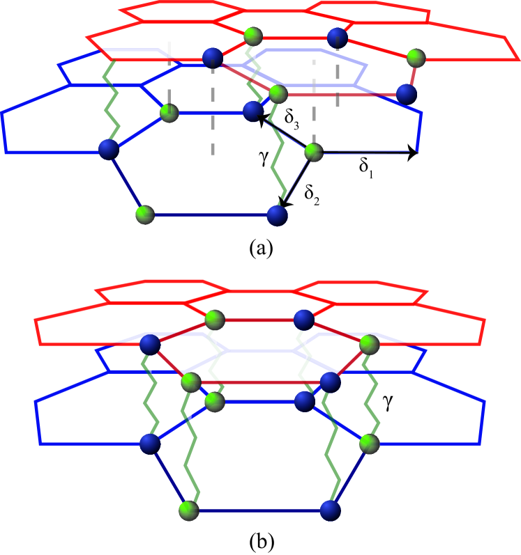
Bilayer graphene is also of intense interest as it too shows an unusual quantum Hall effectGeim and Novoselov (2007); McCann and Fal’ko (2006) and indeed its low energy tight-binding Hamiltonian maps to an equation for chiral fermions with an effective massMcCann and Koshino (2012) based on an interlayer hopping parameter . In addition, it has been seen that bilayer graphene can develop a sizeable band gap which is tunable by charge doping.Ohta et al. (2006) Recent interest in bilayer graphene physics has focused on the large degeneracy at the charge neutrality point which provides opportunity for instabilities leading to new ground states. See Ref. McCann and Koshino (2012) for a summary of the literature on this point and also a general review of the properties of bilayer graphene. The natural form for bilayer graphene is the so-called Bernal or AB-stacking which is the basis of the parent compound graphite from which it is usually derived. Consequently, past work has primarily focused on this stacking configuration. However, more recently, Moiré patterns seen in scanning tunneling microscopy imaging of graphene bilayers and multilayers point to alternative stackings where one layer is rotated by some angle relative to the other.Li et al. (2010); Luican et al. (2011) This is sometimes referred to as twisted or misaligned bilayer graphene. In these systems, the electronic properties are modified at low energy such that monolayer behaviour appears along with a reduced Fermi velocity.Luican et al. (2011) In these systems, it is possible to have regions which are rich in AB-stacking and regions which display mainly AA-stacking. These types of stackings are shown in Fig. 1(a) and (b), respectively. Here, A and B refer to atoms on the two triangular sublattices of the honeycomb lattice and the stacking is in reference to whether the A atom of one plane is stacked over the A or B atom of the other plane. For Bernal AB-stacking only half the atoms are aligned on top of each other and the other half sit over the center of the hexagon in the opposite layer. For AA-stacking all atoms are matched up between the two layers. For very small twist angles, the regions of AA-stacking have been suggested to provide localization effects.de Laissardière et al. (2010, 2012) Very recently, AA-stacked graphene has also attracted interest due to research which has identified such stacking in certain samples, potentially making this another experimentally accessible system to study.Liu et al. (2009); Borysiuk et al. (2011) For AA-stacking there is also the prediction for new ground states to occur, such as antiferromagnetismRakhmanov et al. (2011).
As a result, we are motivated by these developments to examine the dynamical conductivity of doped AA-stacked graphene to elucidate features which would demonstrate unique properties of this system and allow for the identification of characteristic energy scales associated with the band structure. Moreover, as the optical properties of graphene are of considerable importance for technological applications, all variants of graphene are also of potential interest and should be examined. The dynamical conductivity of graphene has been extensively studied theoreticallyAndo et al. (2002); Gusynin and Sharapov (2006); Gusynin et al. (2006); Falkovsky and Varlamov (2007); Peres et al. (2006); Gusynin et al. (2007) and experiments have largely verified the expected behaviourLi et al. (2008); Kuzmenko et al. (2008); Nair et al. (2008); Mak et al. (2008). Likewise, the conductivity for Bernal-stacked bilayer graphene has been predicted theoreticallyAbergel and Fal’ko (2007); Nicol and Carbotte (2008); Nilsson et al. (2008); Koshino and Ando (2009) and observedLi et al. (2009); Zhang et al. (2008); Kuzmenko et al. (2009). There has also been work on magneto-optical conductivity of graphene in which theory and experiment are also in good agreement. Indeed, a review of this literature may be found in Ref. Orlita and Potemski (2010). Some preliminary work on the absorption coefficient of undoped AA-stacked graphene in zero magnetic field has been reportedXu et al. (2010) however most materials naturally occur with charge doping where the Fermi level or chemical potential is away from charge neutrality (). Furthermore, the interesting feature for practical applications is the variation of optical properties with doping, usually achieved through a field effect transistor structure.
In the following, we provide a thorough examination of the finite frequency conductivity for AA-stacking, for both in-plane and out-of-plane response. Unlike a single monolayer, AA-stacked graphene shows a Drude response in the in-plane conductivity at charge neutrality along with Pauli blocking at low frequencies below the onset of a flat interband absorption. This interband absorption splits at finite doping into two interband absorption edges leading to flat universal values associated with one and two layers. In terms of the interlayer hopping energy , the partial optical sum, which is a measure of the transfer of spectral weight, shows distinct behaviour for versus . The perpendicular conductivity has a strong response at at all dopings. This is contrasted with the case for AB-stacking which we also show here as we can also provide an analytical formula for this quantity to add to the literature. Indeed, we have provided analytical formulae in almost all cases and physical understanding of our results are given. We also contrast the AA-stacked case with that for AAA-stacking. Finally, because of the connection between the Dirac nature of graphene and topological insulators (TIs), we also follow-up on a toy-modelPrada et al. (2011) by providing the conductivity for two AA-stacked sheets with spin orbit coupling in one or both planes, potentially mimicking weakly coupled TIs or a TI in proximity to a metallic sheet.
Our paper is organized as follows. In Section II, we review our theoretical calculation for the dynamical conductivity of AA-stacked graphene. Our presentation follows that for AB-stacked bilayer graphene done by Nicol and CarbotteNicol and Carbotte (2008) which uses many-body Green’s function which easily allows for further theoretical development, such as the inclusion of a self-energy from impuritiesNilsson et al. (2008), electron-phonon interactionStauber and Peres (2008); Nicol and Carbotte (2009); Carbotte et al. (2010); Pound et al. (2011a, b, 2012), electron-electron interactionsLeBlanc et al. (2011); Carbotte et al. (2012); Principi et al. (2012), etc. In Section III, we discuss the results of the AA-stacked case, examining both in-plane and perpendicular conductivity and contrasting with the AB-stacked case. We discuss the effect of biasing the bilayer. We also consider the theory for other variations on the AA-stacked case in the subsequent sections. For instance, we examine the case for the AAA-stacked trilayer in Section IV and report results for models with spin orbit coupling in AA-stacked bilayer in Section V. Our conclusions are found in Section VI.
II Theory for AA-stacked bilayer
To derive the optical conductivity of AA-stacked bilayer graphene, we follow the method shown in the work of Nicol and CarbotteNicol and Carbotte (2008) for the case of AB-stacked bilayer graphene. This is based on the Kubo formula for the current-current response function and the many-body Green’s function approach.Mahan (1990) Thus, to begin we must first examine the band structure and provide an expression for the electronic Green’s function. For the case of AA stacking, an A (B) atom in the upper layer is stacked directly above an A (B) atom in the lower layer, see Fig. 1(b), as opposed to the typical Bernal stacking shown in Fig. 1(a).
For AA stacking, the single spin Hamiltonian is given by
| (1) |
The first two terms are the nearest-neighbour intralayer hopping terms for electrons to move within a given plane with hopping energy eV. The two planes are indexed 1 and 2. As a consequence of the geometry of the honeycomb lattice, each sheet has two inequivalent atoms labelled A and B. The operator annihilates an electron which is on an A-atom site with site label in the graphene sheet indexed by . The label indexes the sites of the triangular Bravais lattice. Conversely, creates an electron in sheet on the neighboring site at the position , where is one of three possible nearest-neighbour vectors given by , and . The primitive vectors of the triangular sublattice are and , where with the shortest carbon-carbon distance. The third term in Eqn. (II) corresponds to the interlayer hopping between graphene sheets. The hopping parameter between an A (B) site in one layer and the nearest A (B) site in the other layer is given by which is reported to be about 0.2 eVXu et al. (2010); Lobato and Partoens (2011), which differs in AB-stacked bilayer graphene where it is closer to 0.4 eV. There is also a possibility to hop between an A (B) site in one layer to a B (A) site in the other layer; however, these hopping energies are very smallCharlier et al. (1992); Lobato and Partoens (2011) and thus ignored in our model. The Hamiltonian given in Eqn. (II) transforms to space in the usual wayMahan (1990) and can be written in the following matrix representation:
| (2) |
where and we have used the eigenvector following the notation of McCannMcCann (2006). The band structure is given by the eigenvalues of this matrix. Reflecting the fact that there are now four atoms per unit cell, we obtain the following four energy bands:
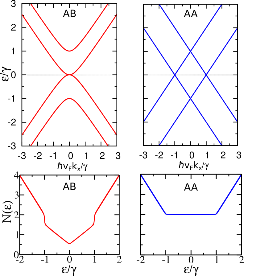
| (3) |
where and 2 and is the energy dispersion for a single sheet of graphene. We essentially have two copies of the band structure of monolayer graphene, one shifted by and the other by , or bonding and antibonding bands, and indeed we will see that this provides part of the physics which enters the dynamical conductivity. As our interest is to understand the conductivity at low energies, we choose to expand around the point of the Brillouin Zone to obtain , where and is the -space angle around the point. The low energy band structure can be seen in Fig. 2 where it is compared to that of the familiar Bernal stacking. As the physics of the conductivity associated with the will be the same as for the point, it is sufficient to work only about the one point in what follows and multiply the result by a factor of two for the so-called valley degeneracy associated with the two points per unit cell.
We can also provide, as others have shownAndo (2011), an analytic expression for the total double spin density of states, :
| (4) |
which results from the sum of two Dirac cone density of states shifted relative to each other by . A plot of the low energy density of states in units of for AA-stacked bilayer graphene is shown in Fig. 2 and is contrasted with that for AB-stackingNicol and Carbotte (2008).
With our Hamiltonian, it is straightforward to determine the Green’s function from . Thus
| (5) |
The only elements of the Green’s function that contribute to our final expressions for longitudinal and perpendicular optical conductivity are , , and . We will only show these elements explicitly:
| (6) |
| (7) |
| (8) |
and
| (9) |
The finite frequency conductivity is calculated through the standard procedure of using the Kubo formulaMahan (1990), where the conductivity is written in terms of the retarded current-current correlation function. From this the real part of the conductivity can be written asNicol and Carbotte (2008)
| (10) |
where we have used the spectral function representation of the Green’s function,
| (11) |
Here and represent the spatial coordinates ,,, is a degeneracy factor, is the Fermi function for temperature and is the chemical potential taken to be positive here but to accommodate for negative values, just needs to replaced by everywhere. Note that we will usually take when referring to the relationship between energy and frequency and restore it when necessary. For our results, we show only the case. For the longitudinal in-plane conductivity, , where
| (12) |
The velocity operator can be evaluated from a Peierls substitution as demonstrated in Ref. Nicol and Carbotte (2008) or from . We can then evaluate the trace, drop the terms that will vanish upon averaging over angle and obtain an expression dependent on the two spectral functions and . In the zero temperature limit, the real part of the longitudinal conductivity is then
| (13) |
In keeping with the low energy expansion of about a single point, the integral over , which in general is over the first Brillouin Zone, is now taken as an integral over a single point. The degeneracy factor is thus , where to account for the sum over spin which has been ignored up until now and to account for a sum over the and points of the Brillouin Zone. Furthermore, the upper limit of the integral is taken to be a large cutoff value typical of momentum associated with the large bandwidth. It is convenient to scale Eqn. (II) by the constant background conductivity of a single sheet of grapheneGusynin et al. (2006) given by . All that remains before we can calculate our conductivity is to specify the necessary spectral function elements. Given our expressions for and and Eqn. (11), we obtain
| (14) |
and
| (15) |
For our numerical work, we use the Lorentzian representation of the delta function, , with a broadening of . The broadening is manifest in the optical conductivity as an effective transport scattering rate of due to the convolution of the two Lorentzian functions in the conductivity formula.
We can also examine the perpendicular conductivity, , associated with transport perpendicular to the graphene sheets. In Eqn. (II), our velocity operator is now ()
| (16) |
where with the interlayer distance. is about 3.6 Å and 3.3 Å for AA- and AB-stacking respectivelyXu et al. (2010); Lobato and Partoens (2011). This leads to the real part of the zero temperature perpendicular conductivity:
| (17) |
with and given by Eqns. (14) and (15), respectively, and
| (18) |
and
| (19) |
with .
III Results for AA-stacked bilayer
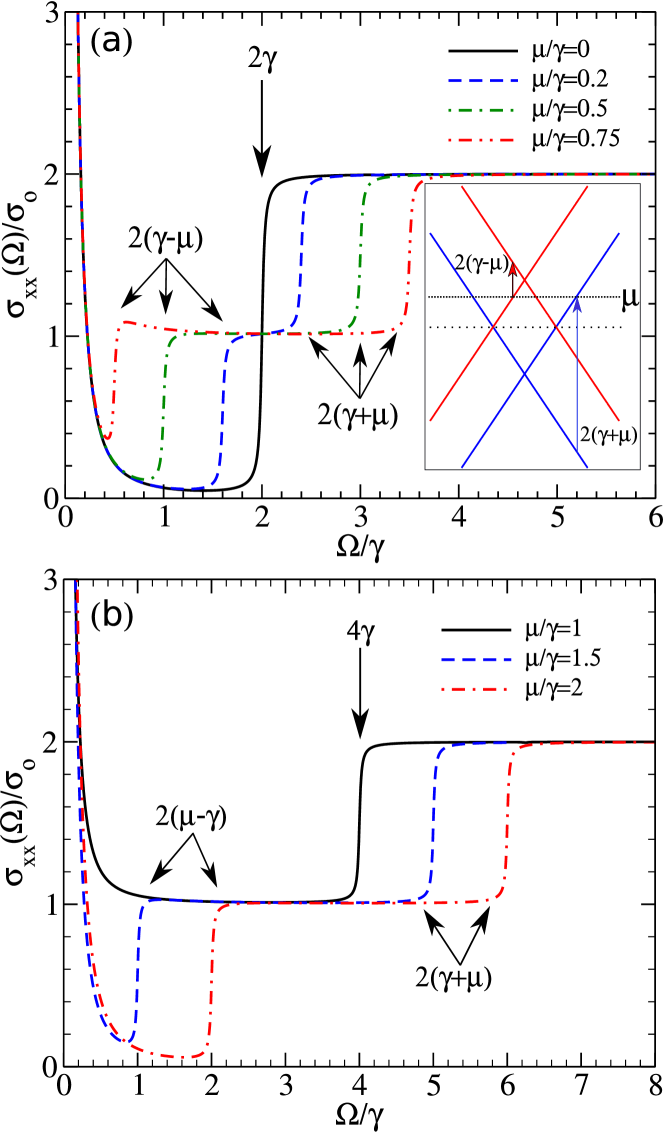
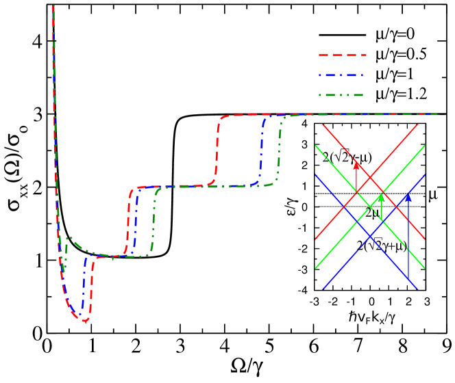
Here we present results for the longitudinal conductivity which is obtained by evaluating Eqn. (II) numerically using the Lorentzian form in place of the delta function and taking the broadening parameter . Fig. 3 shows curves for the case of and (top and bottom frames, respectively). For the case of charge neutrality (), the conductivity displays a Drude response at low frequency due to intraband transitions and a flat interband absorption which commences at . This is quite unlike the case of monolayer graphene which would have had a flat interband response at all frequencies. Here the response is not simply that of two monolayers as one might naively think. This is because the AA-stacked bands are essentially two decoupled graphene monolayer bands which represent bonding and antibonding bands and are shifted relative to each otherAndo (2011) (as emphasized in the inset where the bands are identified with different colors). The matrix elements for the longitudinal conductivity only allow for transitions between like-colored bands.Xu et al. (2010) The transitions must be vertical as the photon is a momentum probe. At charge neutrality, the minimum interband transition that is not Pauli blocked is then and intraband transitions can also now occur due to the Fermi level being located away from the Dirac point of the monolayer band, this latter feature is not present in previous workXu et al. (2010). This emphasizes that knowledge of the band structure as shown in Fig. 2 is insufficient (or may be misleading) to the determination of the allowed absorption transitions and that the matrix elements which know about effects of chirality and bonding/antibonding are important as well.
For finite chemical potential, the Drude persists but now there are two pieces to the interband absorption which onset at and . The behavior is different for versus . For the case of , the Drude conductivity remains completely unchanged and its weight is set by the value of . The interband edge that was at in the case is now split into two edges moving to lower and higher frequency and associated with the onset of allowed transitions for a single monolayer band structure shifted up or down by , respectively. This is emphasized by the AA-stacked band structure shown in the inset of Fig. 3(a) where transitions can only occur within the same colored bands. For the monolayer dispersion shifted down by (blue bands) the lowest interband transition from an occupied state to an unoccupied state occurs at . For the monolayer dispersion shifted up by (red bands), the lowest transition between cones occurs at . Thus at low enough energy, the finite frequency conductivity displays the universal background absorption of a monolayer but at higher frequency there is a step-up to a flat universal background at and the transition between these steps is tunable with the charge doping.
For the case of as shown in Fig. 3(b), the lower edge has disappeared and there is a background conductivity of for and for . However, in this case, the Drude component still remains at very low frequency. For as shown in Fig. 3(b), the lower edge reappears, showing the double step in universal conductivity value and now both edges move to higher frequency with increased . As the area of the conductivity is conserved, the lost weight at finite frequency is found in the Drude which now increases with as one finds in the monolayer case. These characteristic features of the AA-stacked bilayer are quite different from the case of Bernal stackingNicol and Carbotte (2008) and are not at all the expectation of twice the monolayer conductivity either. The presence of the Drude at charge neutrality in the AA-stacked case is different from the monolayer and AB-stacked bilayer where no such feature exists for . These special features of AA-stacked graphene might prove useful for applications where optical response is tuned by doping (or gating) to be like a switch with three settings: off or 0, on at half setting () and on at full setting (). Use of tuning by gating has been demonstrated for graphene terahertz modulators where the intraband transitions are used in this case.Sensale-Rodriguez et al. (2012) Another significance of the result is that for the spectral range between and , one might not be able to separate monolayer from AA-stacked bilayers by optics alone. Overall, the dynamical conductivity is quite distinct from that of AB-stacked bilayer where no such steps occur and the conductivity is not flat in the low frequency spectral range.Abergel and Fal’ko (2007); Nicol and Carbotte (2008)
These results are embodied by a closed algebraic formula for the real part of the longitudinal conductivity for AA bilayer which can be derived at zero temperature from Eqn. (II):
| (20) |
If the delta function here is replaced by a Lorentzian with broadening of , then this formula gives an excellent representation of the numerical results in Fig. 3. It is also possible to derive an expression for the imaginary part of the longitudinal conductivity which is Kramers-Kronig-related to Eqn. (III) by the relation
| (21) |
with , the real part of the conductivity given by Eqn. (III). Hence,
| (22) |
If in the real part is replaced by a Lorentzian form as we have discussed, then instead of the Kramers-Kronig transformation of to , we have transforming to where represents the transport scattering rate rather than the quasiparticle scattering rate that enters the broadened spectral functions .
The issue of optical spectral weight redistribution with variation in chemical potential can be addressed globally by introducing the partial optical sum:
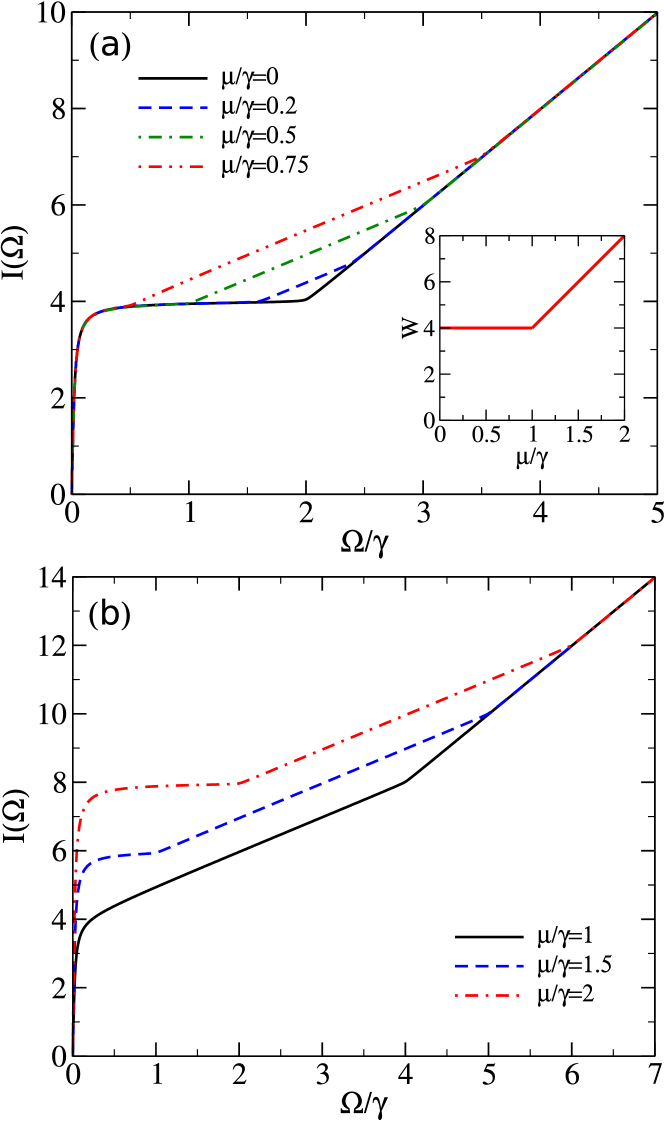
| (23) |
which is defined as the area under the conductivity graph up to energy . For the real part of the longitudinal conductivity, is shown for various values of in Fig. 4. In all cases, at sufficiently high frequency the integrated spectral weight returns to the value (solid black curve of Fig. 4(a)). The inset of Fig. 4 shows the spectral weight of the delta function in the analytic solution, Eqn. III, where we have taken only half the weight of the delta function as only half the function is present for positive frequency. The functions converge to the case at frequencies above once most of the spectral weight from the Drude contribution is integrated as well as the contribution from the interband edges. These curves once again provide an interesting differentiation between the regime, where the Drude weight remains the same and the lower energy kink moves to lower , and the case where the low frequency part of the partial sum increases with and the low energy kink moves to higher . In principle, such a quantity could allow for an experimental determination of based on the transition from the behavior of one regime to the other.
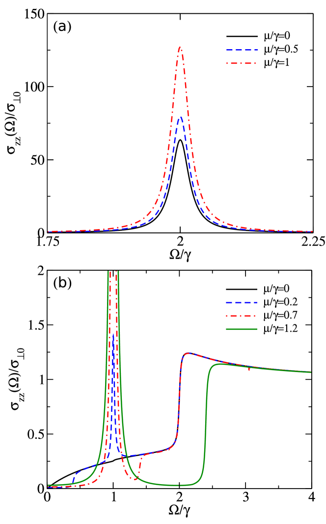
Turning to the perpendicular conductivity, we show the response for the AA- and the AB-stacked bilayer in Fig. 5. The AA-stacked graphene has a strong absorption associated with which is finite at charge neutrality and increases with doping. It is also possible to derive a closed form algebraic formula for the perpendicular conductivity. For AA-stacking we obtain:
| (24) |
and by Kramers-Kronig transformation
| (25) |
for the real and imaginary parts, respectively, where . The physics of this case is as follows. For in-plane conductivity, charge carriers must hop from one sublattice to the other to produce a current, thus in the absorption process, interband transitions are between two bands, each of which reflects the two sublattices by having different chirality label. Hence the transitions shown in the inset of Fig. 3(a) are between two cones which have opposite chirality but the same bonding or antibonding wavefunctions. However, for the interlayer current in the AA-stacked case, the carriers hop between the A(B)-sublattice of one plane to the A(B)-sublattice of the other plane and as a result absorptive transitions for this form of transport will only occur between bands of the same chirality but different bonding which in reference to the inset of Fig. 3(a) would be vertical arrows connecting the parallel bands in this case. As these arrows are always of length , there is only one very strong absorption peak at .
Similar analytical results for AB-stacking at finite doping are, to our knowledge, not in the literature and so we will provide it here for comparison (the equivalent form for AB-stacked in-plane conductivity has been given previously in the literatureNicol and Carbotte (2008); Koshino and Ando (2009)). Some numerical work along with some analytical analysis has been done previously and our results are in agreement with those works.Nilsson et al. (2008); Ando and Koshino (2009) In particular, Ando and Koshino considered polarization effectsAndo and Koshino (2009) which we do not include here. The AB-stacked perpendicular response seen in Fig. 5(b) is quite different from the AA case. Absorption occurs at all frequencies but is on the scale of . An absorption edge occurs at similar to the AA case, although it is weaker by comparison and continues on to higher frequency as it results from transitions between the lowest and highest energy bands of the AB case in Fig. 2, which are the bonding and antibonding bands of the A-B dimer strongly coupled by hopping .McCann and Koshino (2012) Moreover, absorption is seen at all frequencies and at finite doping a very strong peak occurs at much as is seen in the in-plane conductivity for the AB-stacked bilayerNicol and Carbotte (2008). It is not entirely surprising that the perpendicular conductivity displays elements of the in-plane conductivity with the same physical originNicol and Carbotte (2008). The lower energy bands represent hopping between the non-dimer A and B sites in the two planes which must occur by first hopping in the plane to the neighbour site which is part of a dimer, hopping up the dimer bond and then over to the non-dimered site in the second plane.McCann and Koshino (2012) The AA-stacked case does not have this element. For AB-stacking, we derive an analytic formula for the perpendicular conductivity which is:
| (26) |
where
| (27) |
This formula also agrees quite well with the numerical work shown in Fig. 5(b) for various values of the chemical potential, provided the delta function is rewritten as a Lorentzian with broadening of . The expression for the imaginary part is given as:
| (28) |
where is given by Eqn. (III).
We can also examine the effect of adding a bias between the two layers. To do this, we need to include an additional term in our Hamiltonian given by Eqn. (II) of the formNicol and Carbotte (2008)
| (29) |
This bias raises the energy on the lower plane by and lowers the energy on the upper plane by providing an overall bias of . For the case of AB-stacking, this introduces a gap in the energy dispersionMcCann (2006) and provides interesting features to the conductivityNicol and Carbotte (2008). For AA-stacked bilayer, this gives the energy dispersion , where . We can see that this is equivalent to a renormalization of the interlayer hopping parameter of the unbiased system to a value such that and will therefore introduce no new features into the conductivity.
IV Conductivity of an AAA-stacked trilayer
These ideas can also be extended to trilayer graphene. For the case of AAA-stacked trilayer graphene, where A (B) sites in each layer are stacked directly in line with the corresponding sites in the other layers, our Hamiltonian now becomes
| (30) |
where , 2, 3 indexes each of the three layers. Here, we allow the usual nearest-neighbour intralayer hopping and interlayer hopping between the neighbouring planes; again, we have ignored hopping from an A(B) site in one layer to a B(A) site in another layer as well as hopping from an A1(B1) site to an A3(B3) site as these hopping energies are very smallCharlier et al. (1992). Transforming to space, we obtain the following matrix representation:
| (31) |
where we have used the eigenvector . Reflecting the fact that we now have six atoms per unit cell, we obtain the following six energy bands:
| (32) |
where is the energy dispersion of monolayer graphene, equal to at low energy. The first two bands, , are the original graphene bands, the second two bands, indexed , and final two bands, indexed , are monolayer bands shifted by , respectively. A plot of the band structure can be seen in the inset of Fig. 6. From this, we see that the trilayer is like the sum of a monolayer and a bilayer with an interlayer hopping of .
Using the same formalism as before, we can derive an expression for the real part of the zero temperature longitudinal conductivity in terms of the spectral functions; we obtain:
| (33) |
where
| (34) |
| (35) |
| (36) |
and
| (37) |
Several numerical curves for the conductivity can be seen in Fig. 6. For finite , there are three steps in the conductivity each of value , leading to a constant background at high frequency equal to three times that of a single sheet, reflecting the trilayer nature of the system. In each case, there is always an absorption edges at . The other two edges occur at and , where the former decreases with increasing for and then increases for , while the latter always increases with . This is a similar pattern to the AA-stacked case and so the combination of the above confirms that the trilayer acts as the sum of a monolayer plus bilayer. Even at , the flat background of , due to monolayer behavior, is added to the unusual Drude plus interband behavior of the bilayer shown in Fig. 3, but for effective interlayer hopping of . The ability to tune the flat background in the IR spectral region from in steps of by changing the doping is an interesting feature that could possibly be of some advantage to technological applications.
Given Eqn. (IV), an analytical expression for of AAA-stacked trilayer graphene may be written down. It has the expected form:
| (38) |
which stresses the existence of three decoupled and shifted monolayer dispersions where interband transitions are only permitted between the corresponding cones shown in the inset of Fig. 6.
V AA-stacking with Spin Orbit Coupling
Finally, to cover a variety of possible scenarios, we examine the effect of spin orbit coupling (SOC) on AA-stacked bilayer graphene. Such effects in AA- and AB-stacked bilayers were considered by Prada et al.Prada et al. (2011) in the context of studying systems which may manifest a topological insulating phase. These authors have studied both the case of SOC in each plane and SOC in only one plane, the latter case taken to be a toy model for spin-orbit proximity effect. For our purpose here, these considerations illustrate the generic features of opening energy gaps in the AA-stacked band structure at and at the charge neutrality point. Recall from our previous discussion that biasing the bilayer does not open a gap in the AA-stacked case as it does in the AB-stacked case, but SOC will do so.
For a single sheet of graphene including SOC, the tight binding Hamiltonian isKane and Mele (2005)
| (40) |
where, in the continuum limit, and , with , the next-nearest neighbour hopping amplitude. for the Dirac points and and corresponding to the up/down spin component perpendicular to the graphene sheetPrada et al. (2011). With this, the Hamiltonian for the AA-stacked bilayer is
| (41) |
where we have used the eigenvector . When dealing with the case of SOC in both layers, both and are given by Eqn. (40) and is the coupling between the layers, again taken to be
| (42) |
for AA-stacking. Eqn. (41) gives the four energy bandsPrada et al. (2011)
| (43) |
where and 2. These are illustrated in the inset of Fig. 7(b) for a particular point.
While we are interested in , we will forgo providing the explicit details of the calculation as they can be developed by following the procedure already outlined earlier. The expression for given in Eqn. (II) can still be used. However, in lieu of the degeneracy factor , a sum over and should be taken when using Eqn. (41) to calculate the Green’s function. Our velocity operator written in the basis used for this section can be evaluated as before from .
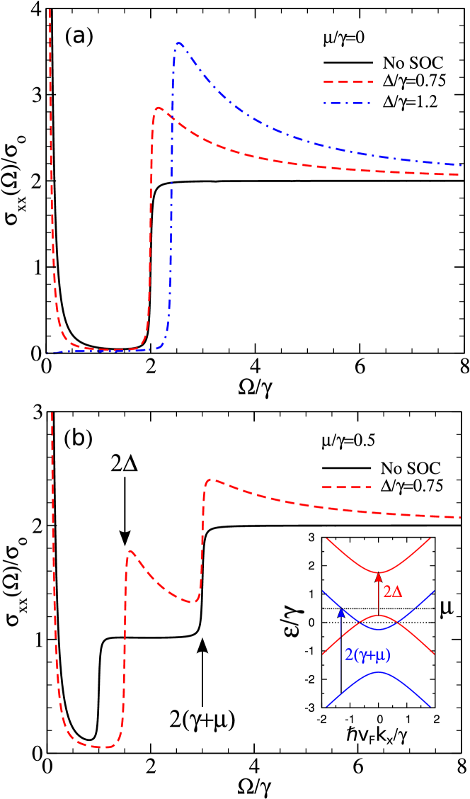
The effect on the real part of the longitudinal conductivity of AA-stacked bilayer graphene when SOC is present in both layers can be seen in Fig. 7 for the case of (a) and (b) . The two shifted monolayer dispersions in the band structure are now gapped by about (see inset of Fig. 7). For and , as shown in Fig. 7(a), there is the usual Drude conductivity and a jump at as in the case of no SOC. However, the shape of this jump is typical of a gapped electronic spectrum which gives rise to a discontinuity in the electronic density of states. Indeed for the monolayer of graphene, such behavior has been calculated.Gusynin et al. (2006) As the frequency increases the usual bilayer background is recovered. The features of the conductivity show that, as in the case of no SOC, transitions are only allowed within each decoupled (like-colored) monolayer band. For the case of , we no longer have the Drude contribution as no states, and therefore no transitions, are available at zero energy. The peak in the conductivity now occurs at and again we can see that we obtain the usual background conductivity for significantly high frequency. We have chosen our values for to be in keeping with the parameters used by Prada et al.Prada et al. (2011), however, in graphene the intrinsic SOC gap is meV and hence . Nonetheless, we have chosen this model to indicate the effect of energy gaps appearing in the band structure. Indeed, other graphene-like systems are now being studied which have much larger predicted SOC gaps, such as silicene ( meV) and germanene ( meV) which can be further tuned by strain or perpendicular electric field.Liu et al. (2011); Drummond et al. (2012) Likewise, a varying mass gap of up to meV has been found in the 3D topological insulator TlBi(S1-xSex)2 by Sato et al.Sato et al. (2011) and the SOC gap in monolayer MoS2 and other group-VI dichalcogenides is on the order of eVXiao et al. (2012). Consequently, the results of this section may be very relevant to future developments in these graphene-like systems.
In Fig. 7(b), the effect of finite doping is considered in comparison with the case of no SOC. For small enough , the SOC curve will track the one without SOC with the exception that there is a peak at each absorption edge reflecting the energy gaps in the band structure at . If , the edge will be at rather than at , and likewise for , there will be only one jump at . A Drude contribution remains provided that . The behavior of the absorption with doping reflects possible transitions between the original shifted monolayer bands subject to the opening of a gap. Mixing between these two monolayer-type bands does not occur. This is illustrated in the inset of Fig. 7(b). The behavior embodied by these figures can be derived analytically and we find it to be:
| (44) |
with
| (45) |
where this last expression is the conductivity for massive Dirac quasiparticlesGusynin et al. (2006); Tse and MacDonald (2010). This formula is in good agreement with the numerical work. Note that for the longitudinal optical conductivity, there is a conservation of spectral weight upon introducing a finite and finite . The corresponding imaginary conductivity is given by
| (46) |
where
| (47) |
If we only keep SOC in one layer, one of the diagonal elements of our Hamiltonian given by Eqn. (41) becomes
| (48) |
and the four energy bands becomePrada et al. (2011)
| (49) |
where or 2. The conductivity for this case can be seen in Figs. 8 and 9 for the case of and finite , respectively. The band structure is plotted in the insets of Fig. 8(a) and (b) for and , respectively. The key energy levels labelled in the insets are given by
| (50) |
where and . Gaps now appear about zero energy and about .
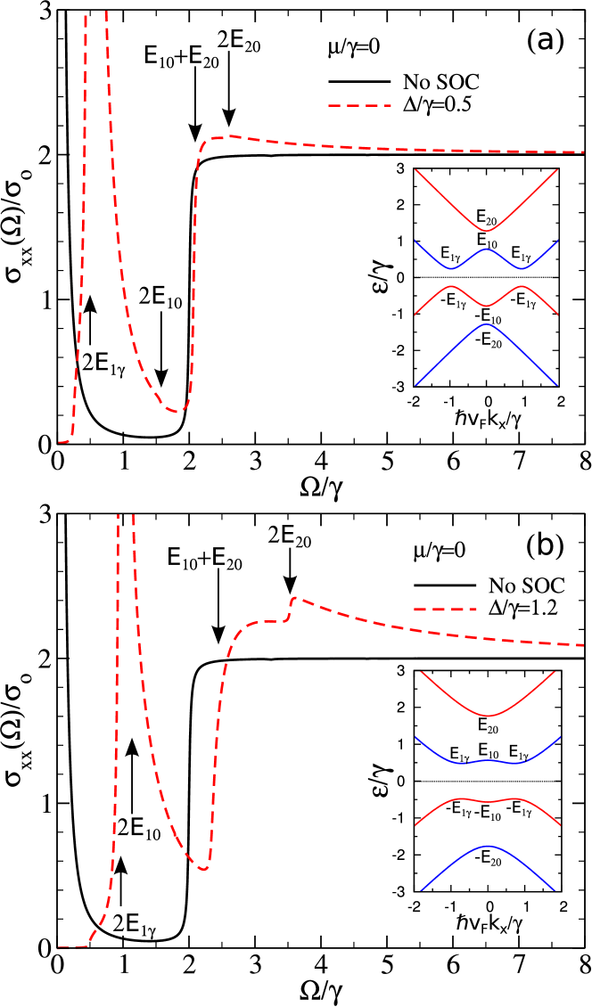
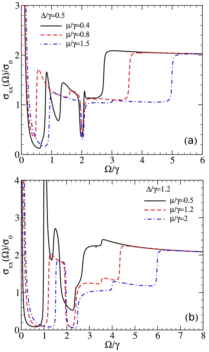
The shape of the optical curves reveals that transitions are now allowed between every band unlike in the previous case with SOC in both layers. In Fig. 8, a strong absorption is seen at (see label in inset to the figure) which is at small values of . The sharpness and strength of this absorption feature is due to the existence of a square root singularity in the electronic density of states at half this energy or . This feature has replaced the Drude absorption due to the gap about zero energy, but very little else changes in Fig. 8(a) from the no-SOC case for small . For shown in Fig. 8(b), further structure appears which can be traced to various transitions in the band structure as has been labelled in the inset. While the behavior is relatively simple for , for finite it is much more complicated. Fig. 9(a) and (b) shows the case for and , respectively, where is varied through key parts of the band structure [refer to the insets of Fig. 8]. While the high frequency behavior is similar to what we have seen for no SOC with an interband absorption edge tracking , the low frequency behavior is very structured. Notable is that the feature at (or for small ) is quickly suppressed by Pauli blocking at finite and there appears to be a deep absorption minimum just on or after . Comparing this figure with Fig. 3 shows that for each value of the underlying structure of the double step for the AA-stacked case with is retained, while the low frequency behavior oscillates about the case. The governing behavior still appears to be dominated by the decoupled monolayer bands however the complicated structure arising from various interband transitions within the different bands is reminiscent of what is found in Bernal-stacked bilayer graphene for finite and an asymmetry gapNicol and Carbotte (2008) which gives rise to similar looking (but not quite the same) band structure. We do not have an analytic form for this complex behavior and one must rely on an examination of the optical transitions available in the band structure to identify the detailed structure. However, it is clear that the case of SOC in only one plane is quite different from that where SOC is in both planes.
VI Conclusions
We have examined the dynamical conductivity for AA-stacked bilayer graphene. The behavior is not simply a case of doubling the conductivity of a graphene monolayer. Indeed the interlayer hopping must appear as an important energy scale. In contrast to the monolayer which is constant at all frequencies for charge neutrality, the bilayer exhibits a Drude conductivity and absorption is Pauli-blocked for frequencies less than . At finite doping, a double step occurs in the interband absorption with onset for each step at and and the behavior is non-monotonic in as a result. The perpendicular response is completely centered on with the absorption peak being very significant at all dopings and increasing with doping. This is unlike the behavior seen in AB-stacked bilayer graphene. Applying a bias across the bilayer does not open an energy gap in the band structure but merely renormalizes the effective interlayer hopping to a greater value. The conductivity of the trilayer exhibits three absorption edges leading to a flat conductivity background which steps up through to . The conductivity in this case is clearly seen to be a sum of that due to a monolayer added to that of a bilayer with interlayer hopping . Including spin orbit coupling in each layer of the AA-stacked bilayer leads to double step behavior where the absorption edges show a peak due to a gap of in the band structure and the location is set by an interplay between the energy scales of chemical potential , and . With spin orbit coupling in only one plane, an absorption peak is found at about and very complicated structure as a function of frequency results at finite although there remains a remnant of the underlying structure of simple AA-stacked bilayer conductivity. As experimental isolation of AA-stacked graphene has been reported and interest in topological insulators with spin orbit coupling is high, this study may be timely for future work in these areas.
Acknowledgements.
We thank James LeBlanc, Jules Carbotte, and Bernie Nickel for helpful discussions. This work has been supported by NSERC of Canada and in part by the National Science Foundation under Grant No. NSF PHY11-25915.References
- Wallace (1947) P. R. Wallace, Phys. Rev. 71, 622 (1947).
- Semenoff (1984) G. W. Semenoff, Phys. Rev. Lett. 53, 2449 (1984).
- Novoselov et al. (2004) K. S. Novoselov, A. K. Geim, S. V. Morozov, D. Jiang, Y. Zhang, S. V. Dubonos, I. V. Grigorieva, and A. A. Firsov, Science 306, 666 (2004).
- Novoselov et al. (2005a) K. S. Novoselov, D. Jiang, F. Schedin, T. J. Booth, V. V. Khotkevich, S. V. Morozov, and A. K. Geim, Proc. Natl Acad. Sci. USA. 102, 10451 (2005a).
- Zhang et al. (2005) Y. Zhang, Y.-W. Tan, H. L. Stormer, and P. Kim, Nature 438, 201 (2005).
- Novoselov et al. (2005b) K. S. Novoselov, A. K. Geim, S. V. Morozov, D. Jiang, M. I. Katsnelson, I. V. Grigorieva, S. V. Dubonos, and A. A. Firsov, Nature 438, 197 (2005b).
- Crassee et al. (2011) I. Crassee, J. Levallois, A. L. Walter, M. Ostler, A. Bostwick, E. Rotenberg, T. Seyller, D. van der Marel, and A. B. Kuzmenko, Nature Phys. 7, 48 (2011).
- Bostwick et al. (2010) A. Bostwick, F. Speck, T. Seyller, K. Horn, M. Polini, R. Asgari, A. H. MacDonald, and E. Rotenberg, Science 328, 999 (2010).
- Castro Neto et al. (2009) A. H. Castro Neto, F. Guinea, N. M. R. Peres, K. S. Novoselov, and A. K. Geim, Rev. Mod. Phys. 81, 109 (2009).
- Abergel et al. (2010) D. S. L. Abergel, V. Apalkov, J. Berashevich, K. Ziegler, and T. Chakraborty, Adv. in Phys. 59, 261 (2010).
- Das Sarma et al. (2011) S. Das Sarma, S. Adam, E. H. Hwang, and E. Rossi, Rev. Mod. Phys. 83, 407 (2011).
- Kotov et al. (2010) V. N. Kotov, B. Uchoa, V. M. Pereira, F. Guinea, and A. H. Castro Neto, (2010), arXiv:1012.3484v2 .
- Geim and Novoselov (2007) A. K. Geim and K. S. Novoselov, Nature Materials 6, 183 (2007).
- McCann and Fal’ko (2006) E. McCann and V. I. Fal’ko, Phys. Rev. Lett. 96, 086805 (2006).
- McCann and Koshino (2012) E. McCann and M. Koshino, (2012), arXiv:1205.6953v1 .
- Ohta et al. (2006) T. Ohta, A. Bostwick, T. Seyller, K. Horn, and E. Rotenberg, Science 313, 951 (2006).
- Li et al. (2010) G. Li, A. Luican, J. M. B. L. dos Santos, A. H. Castro Neto, A. Reina, J. Kong, and E. Y. Andrei, Nature Phys. 6, 109 (2010).
- Luican et al. (2011) A. Luican, G. Li, A. Reina, J. Kong, R. R. Nair, K. S. Novoselov, A. K. Geim, and E. Y. Andrei, Phys. Rev. Lett. 106, 126802 (2011).
- de Laissardière et al. (2010) G. T. de Laissardière, D. Mayou, and L. Magaud, Nano Letters 10, 804 (2010).
- de Laissardière et al. (2012) G. T. de Laissardière, D. Mayou, and L. Magaud, (2012), arXiv:1203.3144v1 .
- Liu et al. (2009) Z. Liu, K. Suenaga, P. J. F. Harris, and S. Iijima, Phys. Rev. Lett. 102, 015501 (2009).
- Borysiuk et al. (2011) J. Borysiuk, J. Soltys, and J. Piechota, J. Appl. Phys. 109, 093523 (2011).
- Rakhmanov et al. (2011) A. L. Rakhmanov, A. V. Rozhkov, A. O. Sboychakov, and F. Nori, (2011), arXiv:1111.5093v1 .
- Ando et al. (2002) T. Ando, Y. Zheng, and H. Suzuura, J. Phys. Soc. Jpn. 71, 1318 (2002).
- Gusynin and Sharapov (2006) V. P. Gusynin and S. G. Sharapov, Phys. Rev. B 73, 245411 (2006).
- Gusynin et al. (2006) V. P. Gusynin, S. G. Sharapov, and J. P. Carbotte, Phys. Rev. Lett. 96, 256802 (2006).
- Falkovsky and Varlamov (2007) L. A. Falkovsky and A. A. Varlamov, Eur. Phys. J. B 56, 281 (2007).
- Peres et al. (2006) N. M. R. Peres, F. Guinea, and A. H. Castro Neto, Phys. Rev. B 73, 125411 (2006).
- Gusynin et al. (2007) V. P. Gusynin, S. G. Sharapov, and J. P. Carbotte, Int. J. Mod. Phys. B 21, 4611 (2007).
- Li et al. (2008) Z. Q. Li, E. A. Henriksen, Z. Jiang, Z. Hao, M. C. Martin, P. Kim, H. L. Stormer, and D. N. Basov, Nature Phys. 4, 532 (2008).
- Kuzmenko et al. (2008) A. B. Kuzmenko, E. van Heumen, F. Carbone, and D. van der Marel, Phys. Rev. Lett. 100, 117401 (2008).
- Nair et al. (2008) R. R. Nair, B. Blake, A. N. Grigeronko, K. S. Novoselov, T. J. Booth, T. Stauber, N. M. R. Peres, and A. K. Geim, Science 320, 1308 (2008).
- Mak et al. (2008) K. F. Mak, M. Y. Sfeir, Y. Wu, C. H. Lui, J. A. Misewich, and T. F. Heinz, Phys. Rev. Lett. 101, 196405 (2008).
- Abergel and Fal’ko (2007) D. S. L. Abergel and V. I. Fal’ko, Phys. Rev. B 75, 155430 (2007).
- Nicol and Carbotte (2008) E. J. Nicol and J. P. Carbotte, Phys. Rev. B 77, 155409 (2008).
- Nilsson et al. (2008) J. Nilsson, A. H. Castro Neto, F. Guinea, and N. M. R. Peres, Phys. Rev. B 78, 045405 (2008).
- Koshino and Ando (2009) M. Koshino and T. Ando, Solid State Commun. 149, 1123 (2009).
- Li et al. (2009) Z. Q. Li, E. A. Henriksen, Z. Jiang, Z. Hao, M. C. Martin, P. Kim, H. L. Stormer, and D. N. Basov, Phys. Rev. Lett. 102, 037403 (2009).
- Zhang et al. (2008) L. M. Zhang, Z. Q. Li, D. N. Basov, M. M. Fogler, Z. Hao, and M. C. Martin, Phys. Rev. B 78, 235408 (2008).
- Kuzmenko et al. (2009) A. B. Kuzmenko, E. van Heumen, D. van der Marel, P. Lerch, P. Blake, K. S. Novoselov, and A. K. Geim, Phys. Rev. B 79, 115441 (2009).
- Orlita and Potemski (2010) M. Orlita and M. Potemski, Semicond. Sci. Technol. 25, 063001 (2010).
- Xu et al. (2010) Y. Xu, X. Li, and J. Dong, Nanotechnology 21, 065711 (2010).
- Prada et al. (2011) E. Prada, P. San-Jose, L. Brey, and H. A. Fertig, Solid State Commun. 151, 1075 (2011).
- Stauber and Peres (2008) T. Stauber and N. M. R. Peres, J. Phys. Condens. Matter 20, 055002 (2008).
- Nicol and Carbotte (2009) E. J. Nicol and J. P. Carbotte, Phys. Rev. B 80, 081415(R) (2009).
- Carbotte et al. (2010) J. P. Carbotte, E. J. Nicol, and S. G. Sharapov, Phys. Rev. B 81, 045419 (2010).
- Pound et al. (2011a) A. Pound, J. P. Carbotte, and E. J. Nicol, Europhys. Lett. 94, 57006 (2011a).
- Pound et al. (2011b) A. Pound, J. P. Carbotte, and E. J. Nicol, Phys. Rev. B 84, 085125 (2011b).
- Pound et al. (2012) A. Pound, J. P. Carbotte, and E. J. Nicol, Phys. Rev. B 85, 125422 (2012).
- LeBlanc et al. (2011) J. P. F. LeBlanc, J. P. Carbotte, and E. J. Nicol, Phys. Rev. B 84, 165448 (2011).
- Carbotte et al. (2012) J. P. Carbotte, J. P. F. LeBlanc, and E. J. Nicol, Phys. Rev. B 85, 201411(R) (2012).
- Principi et al. (2012) A. Principi, M. Polini, R. Asgari, and A. H. MacDonald, (2012), arXiv:1111.3822 .
- Mahan (1990) G. D. Mahan, Many Particle Physics (Plenum, New York, 1990).
- Lobato and Partoens (2011) I. Lobato and B. Partoens, Phys. Rev. B 83, 165429 (2011).
- Charlier et al. (1992) J.-C. Charlier, J.-P. Michenaud, and X. Gonze, Phys. Rev. B 46, 4531 (1992).
- McCann (2006) E. McCann, Phys. Rev. B 74, 161403(R) (2006).
- Ando (2011) T. Ando, J. Phys.: Conf. Ser. 302, 012015 (2011).
- Sensale-Rodriguez et al. (2012) B. Sensale-Rodriguez, R. Yan, M. M. Kelly, T. Fang, and K. Tahy, Nature Commun. 3, 780 (2012).
- Ando and Koshino (2009) T. Ando and M. Koshino, J. Phys. Soc. Jpn. 78, 104716 (2009).
- Kane and Mele (2005) C. L. Kane and E. J. Mele, Phys. Rev. Lett. 95, 226801 (2005).
- Liu et al. (2011) C.-C. Liu, W. Feng, and Y. Yao, Phys. Rev. Lett. 107, 076802 (2011).
- Drummond et al. (2012) N. D. Drummond, V. Zólyomi, and V. I. Fal’ko, Phys. Rev. B 85, 075423 (2012).
- Sato et al. (2011) T. Sato, K. Segawa, K. Kosaka, S. Souma, K. Nakayama, K. Eto, T. Minami, Y. Ando, and T. Takahashi, Nature Phys. 7, 840 (2011).
- Xiao et al. (2012) D. Xiao, G.-B. Liu, W. Feng, X. Xu, and W. Yao, Phys. Rev. Lett. 108, 196802 (2012).
- Tse and MacDonald (2010) W.-K. Tse and A. H. MacDonald, Phys. Rev. Lett. 105, 057401 (2010).