Graphene superlattice with periodically modulated Dirac gap
Abstract
Graphene-based superlattice (SL) formed by a periodic gap modulation is studied theoretically using a Dirac-type Hamiltonian. Analyzing the dispersion relation we have found that new Dirac points arise in the electronic spectrum under certain conditions. As a result, the gap between conduction and valence minibands disappears. The expressions for the positions of these Dirac points in -space and threshold value of the potential for their emergence were obtained. Also, the dispersion law and renormalized group velocities around the new Dirac points were calculated. At some parameters of the system, we have revealed interface states which form the top of the valence miniband.
pacs:
71.10.Pm, 73.21.-b, 81.05.U-I Introduction
During for the last years extremely much attention was paid to the electronic properties of graphene (see Ref.1 for the review). Such interest results, in particular, from the fact that physics of the low-energy carriers in graphene is governed by a Dirac-type Hamiltonian. The band structure of an ideal graphene sheet has no energy gap. As a consequence, Dirac electrons become massless, and reveal unusual properties such as perfect transmission at normal incidence through any potential barrier (the Klein paradoxKlein ; Kat ), trembling motion (or ZitterbewegungGM ), etc. Because of the Klein effect, an electrostatic potential cannot confine electrons in graphene. This property of graphene impedes its use in electronic devices.Geim However, as has been shown,Martino it is possible to confine massless Dirac particle in graphene sheet by inhomogeneous magnetic field. The confinement can be also achieved by combining electric and uniform magnetic fields.N7 ; N8 Meanwhile, Dirac electrons can be localized electrostatically in a gapped graphene.
The gap can be induced by substrate or strain engineering as well as by deposition or adsorption of molecules on a graphene layer. For example, two carbon sublattices of graphene placed on top of hexagonal boron nitride (-BN) become nonequivalent due to their interaction with the substrate. The band-structure calculations within the local-density approximation for this system gives a gap not less than 53 meV.Gio A hydrogenated sheet of graphene (graphane) is a semiconductor with a gap of the order of a few eV.Leb
Besides, it is possible to modulate spatially the gap (i.e. the particle’s mass) in graphene. It was shown that the spatial mass dependence leads to suppression of Klein tunneling and induces confined states.Peres ; Nori The required gap modulation can be created, for instance, in graphene placed on a substrate fabricated from different dielectrics. It is also possible to use for this purpose an inhomogeneously hydrogenated graphene or graphene sheet with nonuniformly deposited CrO3 molecules. Correspondingly, one can fabricate different graphene heterostructures with the gap discontinuity. In particular, graphene-based superlattice (SL) can be formed due to the periodic modulation of the band gap.
Recently, electronic structure of graphene under external periodic potential has been the subject of numerous studies.B1 ; B2 ; Yang ; Fertig ; Vas2 ; B6 ; B7 ; B8 ; B9 ; B10 ; B11 ; I1 ; I2 ; I3 ; I4 ; I5 Increasing interest in graphene SLs results from the prediction of possible engineering the system band structure by the periodic potential, which opens new ways for fabrication of graphene-based electronic devices. The graphene SLs have been realized experimentally. For example, graphenes grown epitaxially on metal surfacesI1 ; I2 ; I3 ; I4 demonstrate SL patterns with about several nanometers SL period. Recent scanning tunneling microscopy studiesI5 of corrugated graphene monolayer on Rh foil show that the quasi-periodic ripples generate a weak one-dimensional electronic potential in graphene leading to emergence of the SL Dirac points. It was as well shown theoretically that a one-dimensional periodic potential really affects the transport properties of graphene. For instance, the Kronig-Penney (KP)-type electrostatic potential induces strong anisotropy in the carrier group velocity around the Dirac pointB1 ; Vas2 leading to the so-called supercollimation phenomenon.B1 ; B2 Besides, in the SL spectrum new (extra) Dirac points appear in Brillouin zone. These features has been also examined for the different types of graphene SL including the magnetic KP-SL with delta-function magnetic barriers.B6 ; B7 ; B8 ; B9 ; B10 ; B11 In Ref.19 the first-principles studies of the electronic structure of graphene-graphene SL modeled with a repeated structure of pure and hydrogenated graphene (i.e., graphane) strips has been performed. It was found that unlike other graphene nanostructures, the hydrogenated graphene SLs exhibit both direct and indirect band gaps.
In this paper we focus on the electronic states in graphene-based SL with periodically modulated gap and relative band shift (potential) where the gap and potential are piecewise constant functions of . The model of such SL has been considered earlier.Rat However, no detailed examination of the electronic structure in such type SLs in a wide range of the system parameters has been carried out. In particular, we have first found that the considered SL can be gapped or gapless depending on the band shift. We analyze in detail the SL with equal widths of the gapless and gapped graphene fractions, and show that the forbidden miniband exists up to some threshold value corresponding to the first emergence of the Dirac-like point at . When the potential exceeds , this Dirac-like point disappears, opening the minigap at . At the same time, two extra Dirac points arise in symmetric positions on the axis. This scenario differs from the one realized in graphene SL formed by the electrostatic potential,Vas2 where the original Dirac point (at ) always exists. Further increasing leads to emergence of a new pair of the Dirac points from the origin . The dispersion in the vicinity of these points appears to be anisotropic, indicating an anisotropic renormalization of the group velocity. We also show that interface states can exist in the gap-induced SL in contrast to the SL formed by a Kronig-Penney-type electrostatic potential. For this case the relevant conditions and values of the system parameters were obtained.
II Dirac particle in graphene superlattice
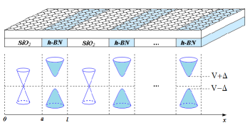
Let us consider one-dimensional (1D) graphene superlattice with period formed by position-dependent gap and band shift. As was shown in Ref.29, such structure can be realized, e.g., on the base of graphene deposited on a strip substrate combined from silicon oxide and -BN (Fig.1). The SL electronic structure in the vicinity of -point of the Brillouin zone is described by the Dirac-like Hamiltonian
| (1) |
where is the momentum operator, are the Pauli matrices, is a unit matrix, is the Fermi velocity, and , are periodic functions equal to and , respectively, at , and zero at . Here, the potential defines the shift of the forbidden band center in the gapped graphene with respect to the Dirac point in the gapless grapheneRat ; Silin (see Fig.1). Generally speaking, the Fermi velocity can differ in graphene modifications placed on different substrates. In our model, however, we neglect the dependence on supposing cm/s in both graphene fractions.
The Kronig-Penney model considered here as applied to graphene SL is also used in many other physical problems including, e.g., modeling of semiconductor SLs or relativistic particle dynamics. Although master equations describing the single-particle evolution differ for all the mentioned systems, explicit forms of the dispersion relations obtained within the framework of the Kronig-Penney model resemble to each other. Nevertheless, individual features of these systems result in qualitative distinctions in their band structures. For instance, the dispersion relation for 1D relativistic electron in Kronig-Penney potentialStrange ; Kel is similar to the one obtained in this paper (see Eq.(9) below) for 2D electrons in 1D graphene SL. In our case, however, the periodic potential in Dirac-like equation is formed by two terms having different meanings from the point of view of relativistic physics. The relative band shift can be treated as the time-like vector component while the band-gap represents a scalar potential. This circumstance together with the two-dimensionality of the electron gas provide new fundamental properties of the SL electronic structure (such as appearance of extra Dirac points), which will be discussed in detail in section III.
The Dirac equation
| (2) |
admits the solutions , where the two-component spinor envelope function satisfies the equation
| (3) |
with
| (4) |
The formal solution of Eq.(3) is
| (5) |
where is the spatial ordering operator.Kel ; Ar This expression can be simplified as
| (6) |
if both points and belong to the space-homogeneous region.
In this case it is convenient to define the matrix
| (7) |
Here, the matrix is defined by Eq.(4) where if , and , if . The straightforward calculation yields , where . Therefore, all even powers in the Taylor series of the exponential function in Eq.(7) will be proportional to the unit matrix while all odd powers will be proportional to the matrix itself. This leads to the following expression:
| (8) |
where .
We can now find that , where . Note, that , and, consequently, as well. This equality and the Bloch condition (here, is the Bloch wave vector) yield the dispersion relation for the 1D graphene-based SL. Using Eq.(8) one can find . Accordingly, the resulting dispersion equation reads
| (9) |
with , . At , the wave number is imaginary and the allowed energies are given by Eq.(9) with replaced by .
Eq.(9) for the allowed energies was obtained also in Ref.29 via wave function matching. However some results of this work concerning the miniband structure and existence of the interface states seem questionable. Below we discuss these issues in detail. Note that at , Eq.(9) coincides with the one found for single-layer graphene in a periodic piecewise constant potential .Ar ; Vas1 ; Vas2
III Electronic structure
The miniband structure depends on the system parameters as well as on the -component of the wave vector. As seen from the Eq.(9), the dispersion relation is invariant with respect to the simultaneous replacements , . Therefore, in what follows we shall consider, for definiteness, only nonnegative values of the relative band shift: . When , the energy spectrum is completely symmetric related to the value corresponding to the original Dirac point in the gapless graphene. In this case the two first minibands symmetrically situated above and below the point are the conduction and valence ones, respectively. As increases, the conduction and valence minibands gradually shift up. Below we shall concentrate on these two minibands only, assuming the Fermi level to be in between at any .
The electron and hole energies as functions of at , meV for different values of the potential and widths are plotted in Fig.2(a). The parameters we choose are appropriate for graphene. Thick and thin solid lines correspond to and meV, respectively, and . When becomes nonzero the electron (conduction) and hole (valence) minibands shift up, and the electron miniband turns out to be a little narrower than the hole one. This is, presumably, due to the fact that at chosen values of the parameters the electron miniband completely forms under the barrier at : , while the hole-miniband energies mainly belong to the over-barrier region .
The energy branches in the conduction and valence minibands at , meV is shown with dashed line. We can see that, as the gapped graphene fraction in the SL increases, the electron-hole minigap increases too. Nevertheless, in any case, at the minigap cannot exceed the gap value .text Indeed, it is clear that if the whole graphene layer is gapped, i.e. , the forbidden miniband should be (at =0).
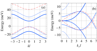
Figure 2(b) illustrates the dependence of the electron and hole energies on at different and , and , , nm. We show only semiaxis because of the symmetry in the dispersion law [Eq.(9)]. The energies in the figure are counted from the minigap center (its position determined at depends on ) for meV (thin solid line) at meV. In other cases the energy origin coincides with the contact or cone-like point energy. Our calculations demonstrate a monotonous expansion of the forbidden miniband with increasing (thin solid line in Fig.2(b)) until becomes greater than some threshold value (for chosen set of parameters meV). When (thick solid line in Fig.2(b)), the electron and hole energy branches touch each other at closing the minigap. When exceeds , the minigap at opens, but two extra Dirac points appear in symmetric positions on the -axis (solid line in Fig.2(b)), and never then vanish. Thus, beginning with the gap-induced SL becomes gapless.
This feature of the theoretically predicted dependence of the SL minigap on , in fact, can be observed by spectroscopic methods. In order to vary the parameter it is possible to apply additional nano-gate potential to the gapped graphene fractions in the SL. Closing the minigap accompanied by the disappearance of the absorption edge and appearance of the contact point in the SL spectrum allows one, in turn, to determine experimentally the threshold value .
Further increase of results in formation of new additional cone-like Dirac points which originate from . Such a behavior is not unique. As was shown in Refs 15-17 for gapless graphene, the new Dirac points can emerge in the presence of a sinusoidal or squarewell SL potential. A simple analytical expression for the positions of these points in -space has been obtained by different research groups.Vas2 ; Ar In our model, however, in contrast to the SLs discussed in the works quoted above, the Dirac point being a prototype of the original Dirac point at arises at certain finite values of equal to (defined by the zeroes of , see Eq.(12) below) with being positive integer. Note that, coincides with the threshold potential value .
It is clearly seen from Fig.2(b) that extra Dirac point located at for (dashed line) remains also in the case at the same values of when . However, the location of the Dirac point in this case slightly shifts towards zero with increasing. In order to find the location of the Dirac points in -space we note that and coincide at
| (10) |
Correspondingly, Eq.(9) at , and turns into
| (11) |
Obviously this equation is satisfied if ( is integer and differs from zero), which leads to , where
| (12) |
One can check that for , the right side of Eq.(9) has local maximum (equal to unity) at and . This means coincidence of conduction and valence miniband edges.
According to Eq.(12), in general case, when the ratio is not integer, the number of Dirac points symmetrically situated around is given by
| (13) |
where denotes an integer part. One of the contact points is always located at if . In this case , and the total number of Dirac points is odd: .
Thus, now we can write analytically the inequality for the system parameters corresponding to the formation of the gapless SL. Evidently, the gap separating the conduction and valence minibands vanishes if
| (14) |
The case of the rigorous equality in Eq.(14) corresponds to the threshold value of the potential: (the positive root of the quadratic equation).
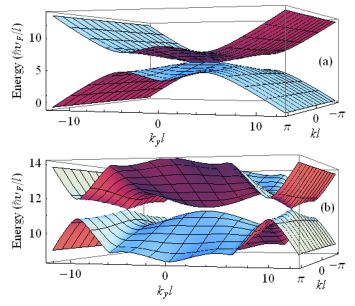
Solving Eq.(9) numerically we have found the dispersion law presented in Fig.3 for (panel (a)) and (panel (b)). It is seen that when there is the only contact point in the electronic spectrum, having no conical shape. When , two cone-like Dirac points exist at , , and . Let us further consider the dispersion relation in the nearest vicinity of the contact and cone-like Dirac points.
We start with the contact point arising at , , and . For this purpose one has to expand the terms in Eq.(9) at into the Taylor series up to the lowest powers of , , and . As an example, below we consider the case , i.e. . After some algebra one obtains the dispersion relation in the following form:
| (15) |
where we have introduced dimensionless energy , and parameters and . The signs ”+” and ”” correspond to the electrons and holes, respectively. Evidently, the energy surface around the only contact point, indeed, has no conical form. The first term in the right side of Eq.(15) defines an asymmetry of the conduction and valence minibands related to . If (in this case ), the conduction and valence minibands become symmetric near the contact point. According to Eq.(15) at , the edges of the conduction and valence minibands are parabolic along -axis:
| (16) |
As a result, the dispersion along is almost flat. In the limiting case , the coefficient before becomes proportional to (i.e. ). Note that in the SL based on a gapless graphene the dispersion curves at also demonstrate a nonlinear behavior, where, however, dispersion is defined by the third power of the -component of the wave vector: .Vas2
Basing on Eq.(15) we can now determine the velocity components , in the vicinity of the contact point at . Calculating the derivatives one gets
| (17) |
| (18) |
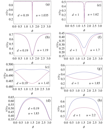
The obtained expressions exhibit strong anisotropy of the electron and hole velocities in -plane, which is clearly seen from the dependence of the absolute value on the polar angle introduced with standard relations: , , where . The dependence is sensitive to the induced gap (or ) as Fig.4 shows. When (panel (a)), is close to for all angles except for the nearest vicinity of where narrow dip in the dependence occurs. As increases, monotonously decreases in whole, keeping the dip that becomes a little wider as seen in panel (e). Such a dip is caused by the lens-like shape of the energy surfaces both for the electrons and holes as described by Eq.(15). In this case, the component is much greater than for all except for the narrow domain near the ”lens” edge, where is close to . Within this domain both and are small as follows from Eqs (17) and (18). Note also that, the electron and hole velocities and , in fact, coincide at the considered values of .
Finalizing discussion of the energies and group velocities near the contact point we would like to emphasize as well that, expressions similar to Eqs (15) - (18) can be easily obtained for . In this case one should simply replace by in all the expressions. Consequently, the dispersion in direction flattens compared to the one described by the Eq.(16).
When , which implies that , the situation is different. In this case introducing small deviation , it is easy to find from Eq.(9) the dispersion law in the form:
| (19) |
Here, the parameters , , and are defined as
| (20) |
where the dimensionless potential is always greater than if .
Provided that slightly exceeds (), the energy surface becomes a cone elongated in -direction. As increases, the cone gradually turns into the isotropic one, and then becomes elongated in -direction. Thus, the dispersion law around the new cone-like Dirac points in the considered SL has strong anisotropy dependent on in contrast to the original Dirac point in a gapless graphene. Similar behavior takes place in the graphene SL formed by -modulation at .Vas2 In our case, however, in contrast to the mentioned work, the cone is always tilted due to the presence of the linear in term in the dispersion relation [Eq.(19)]. The cone-axis obliquity is defined by the coefficient which tends to zero when .
The anisotropy of the dispersion law naturally manifests itself in the dependencies of the electron and hole velocities on . Because of the cone-type shape of the energy surface, the velocity components
| (21) |
do not depends on but exclusively on . Due to the cone tilt, -component has nonzero mean value
| (22) |
being the same for the electrons and holes.
In Fig.4 we have plotted the relation around the cone-like Dirac point with for the electrons and holes as function of the polar angle for various () at two values of the gap: meV (, panels (b) - (d)), and meV (, panels (f) - (h)). Provided that the parameter is close to zero, and the Dirac-cone tilt is negligibly small. As a result, and differ insignificantly. The electron and hole velocities vary strongly when strongly differ from (panels (b) and (d), where equals 165.15 meV and 253.23 meV, respectively). This corresponds to the Dirac cone elongated in -direction if (panel (b)) or in -direction in the opposite case (panel (d)). When (this is so, e.g., at meV) the cone becomes almost isotropic. Consequently, and remain almost constant and equal to (panel (c)). At greater the cone tilt differently influences and , as shown in panels (f) - (h), where equals 235.2 meV, 256 meV, and 304.4 meV, respectively. The behavior of the electron and hole velocities in this case is qualitatively similar to that takes place at . However the difference is no longer small.
We do not discuss here the case . We expect that Dirac points appear in this case too. However, the electron-hole miniband profile should be significantly asymmetric related to the Fermi level as it was in -modulated SL.Vas2
IV Interface states
As was shown by Ratnikov and SilinRS interface states can exist in graphene-based heterojunctions. It was found that interface states result from the crossing of dispersion curves of gapless and gapped graphene modifications. Meanwhile, in graphene-based superlattices, formation of interface minibands was considered to be impossible.Rat In contrast to this statement we have found that the interface states can arise under certain conditions discussed below. Since the wave functions of these states behave as exponentials along -axis, the wave vectors and should be imaginary, so that
| (23) |
In this case Eq.(9) transforms into
| (24) |
with , .
Evidently the solution of this equation can exist only if
| (25) |
Since the left side of this expression is positive (see Eq.(23)) the allowed values of the energy should be negative if and vice versa. It is not difficult to show that the inequalities (23) and (25) have the solutions when and differ from zero, , and .
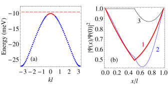
As a result, at interface states can be realized exclusively inside the hole miniband, while the electron miniband consists of oscillating states only, whose wave functions oscillate, at least, within . In Fig.5(a) the hole miniband of the SL with nm is plotted for meV, meV, and . Upper narrow slice of the valence miniband depicted by solid line is formed by the interface states. Indeed, it is possible to verify that any energy value from this range obey the inequalities (23) and (25) for the above parameters. Dashed (red) line in the figure shows the interface energy level for an isolated heterojunction.RS
Fig.5(b) represents the squared absolute values of the hole wave functions corresponding to the valence miniband whose profile is shown in Fig.5(a) at . We plot the probability density for some interface state (curve 1) with the energy belonging to the top slice of the valence miniband (solid line in panel (a)). It is seen that exponentially drops towards the interface . For comparison, in Fig.5(b) we plot also the probability densities for two other states from the valence miniband (curves 2 and 3) oscillating inside the gapless region . Solving the Dirac equation at it is not difficult to show that is always constant within the gapless region (curve 3). Note also, that in this case the probability density must be symmetric with respect to the points and , as shown in the figure.
V Concluding remarks
We have considered the simple model of a one-dimensional SL in which the gap and potential profile are piecewise constant functions. In the framework of this model the dispersion relation for Dirac electrons was obtained, and the structure of low-energy minibands was investigated depending on the potential and other parameters of the SL.
It was found that beginning with some critical value of the relative band shift the new contact or cone-like Dirac points appear in the SL spectrum. As a result, at the SL becomes gapless. The contact point exists only at certain but always at , while the cone-like points are situated symmetrically related to at some finite when . In the case where the widths of the gapless and gapped graphene strips in the SL are equal, we found the positions of the Dirac points in -space and obtained an expression for the threshold potential value corresponding to their appearance. The dispersion relation and carrier velocities were analyzed in the vicinity of the contact and cone-like Dirac points.
Appearance of new Dirac points at is typical as well for SL induced by the potential modulation of a gapless graphene.Ar ; Vas2 ; Chiu ; Yang ; Fertig Thus, one may conclude that such a reconstruction of the electron spectrum in a certain extent represents a universal property of graphene-based superlattices.
It should be noted that the description of the SL energy spectrum in our work was carried out within the framework of a one-electron picture. Recent theoreticalC1 ; C2 ; C6 and experimentalC3 ; C4 ; C5 investigations of many-particle problem in graphene show that one of the most important consequences of the electron-electron interaction can be the Fermi velocity renormalization. Such a renormalization, presumably, results in different values of in gaplessC6 and gappedC7 graphene fractions, which should, of course, modify the basic dispersion relation [Eq.(9)]. Nevertheless, there are no yet any rigorous quantitative estimations of the renormalization effect, and experimentally obtained value of is usually close to cm/s. Here, we performed our calculations assuming the difference in -values in both graphene fractions to be negligibly small.
Finally, we found that the interface states can exist in the gap-induced SL at certain conditions.
VI Acknowledgments
This work was supported by the Russian Foundation for Basic Research (Grants No 11-02-00960 and 13-02-00784) and Russian Ministry of Education and Science (Contract No 07.514.11.4147).
References
- (1) A.H. Castro Neto, F. Guinea, N.M.R. Peres, K.S. Novoselov, and A.K. Geim, Rev. Mod. Phys. 81, 109 (2009).
- (2) O. Klein, Z. Phys. 53, 157 (1929).
- (3) M.I. Katsnelson, K.S. Novoselov, and A.K. Geim, Nature Phys. 2, 620 (2006).
- (4) G.M. Maksimova, V.Ya. Demikhovskii, and E.V. Frolova, Phys. Rev. B 78, 235321 (2008); T.M. Rusin and W. Zawadzki, Phys. Rev. B 80, 045416 (2009).
- (5) A.K. Geim and K.S. Novoselov, Nat. Matter 6, 183 (2007).
- (6) A. De Martino, L. Dell Anna, and R. Egger, Phys. Rev. Lett. 98, 066802 (2007).
- (7) G. Giavaras, P.A. Maksym, and M. Roy, J. Phys.: Condens. Matter 21, 102201 (2009).
- (8) G. Giavaras and F. Nori, Phys. Rev. B 85, 165446 (2012).
- (9) G. Giovannetti, P.A. Khomyakov, G. Brocks, P.J. Kelly, and J. van den Brink, Phys. Rev. B 76, 073103 (2007).
- (10) S. Lebegue, M. Klintenberg, O. Eriksson, and M.I. Katsnelson, Phys. Rev. B 79, 245117 (2009).
- (11) N.M.R. Peres, J. Phys.: Condens. Matter 21, 095501 (2009).
- (12) G. Giavaras and F. Nori, Appl. Phys. Lett. 97, 243106 (2010); G. Giavaras and F. Nori, Phys. Rev. B 83, 165427 (2011).
- (13) C-H. Park, Y-W. Son, L. Yang, M.L. Cohen, and S.G. Louie, Nature Phys. 4, 213 (2008).
- (14) C-H. Park, Y-W. Son, L. Yang, M.L. Cohen, and S.G. Louie, Nano Lett. 8, 2920 (2008).
- (15) C-H. Park, Y-W. Son, L. Yang, M.L. Cohen, and S.G. Louie, Phys. Rev. Lett. 103, 046808 (2009).
- (16) L. Brey and H.A. Fertig, Phys. Rev. Lett. 103, 046809 (2009).
- (17) M. Barbier, P. Vasilopoulos, and F.M. Peeters, Phys. Rev. B 81, 075438 (2010).
- (18) F. Guinea and T. Low, arXiv:1006.0127v1.
- (19) J.-H. Lee, J.C. Grossman, Phys. Rev. B 84, 113413 (2011).
- (20) L. Dell Anna and A. De Martino, Phys. Rev. B 79, 045420 (2009).
- (21) M. Ramezani Masir, P. Vasilopoulos, and F.M. Peeters, Phys. Rev. B 79, 035409 (2009).
- (22) L. Xu, J. An, and C.-D. Gong, Phys. Rev. B 81, 125424 (2010).
- (23) V.Q. Le, C.H. Pham, and V.L. Nguyen, J. Phys.: Condens. Matter 24, 345502 (2012).
- (24) S. Marchini, S. Günther, and J. Wintterlin, Phys. Rev. B 76, 075429 (2007).
- (25) A.L. Vázquez de Parga, F. Calleja, B. Borca, M.C.G. Passeggi, Jr., J.J. Hinarejos, F. Guinea, and R. Miranda, Phys. Rev. Lett. 100, 056807 (2008).
- (26) P.W. Sutter, J.I. Flege, and E.A. Sutter, Nature Mater. 7, 406 (2008).
- (27) D. Martoccia, P.R. Willmott, T. Brugger, M. Björck, S. Günther, C.M. Schlepütz, A. Cervellino, S.A. Pauli, B.D. Patterson, S. Marchini, J. Wintterlin, W. Moritz, and T. Greber, Phys. Rev. Lett. 101, 126102 (2008).
- (28) H. Yan, Z.-D. Chu, W. Yan, M. Liu, L. Meng, M. Yang, Y. Fan, J. Wang, R.-F. Dou, Y. Zhang, Z. Liu, J.-C. Nie, and L. He, arXiv:1209.1689.
- (29) P.V. Ratnikov, JETP Lett. 90, 469 (2009).
- (30) P.V. Ratnikov and A.P. Silin, JETP 114, 512 (2012).
- (31) P. Strange, Relativistic Quantum Mechanics (section 9.4), Cambridge University Press 1998.
- (32) B.H.J. McKellar and G.J. Stephenson, Phys. Rev. A 36, 2566 (1987).
- (33) D.P. Arovas, L. Brey, H.A. Fertig, E.-A. Kim, and K. Zeigler, New Journal of Physics 12, 123020 (2010).
- (34) M. Barbier, F.M. Peeters, P. Vasilopoulos, and J.M. Pereira, Phys. Rev. B 77, 115446 (2008).
- (35) The author of Ref.29 asserts that the minigap can several times exceed the gap value .
- (36) P.V. Ratnikov and A.P. Silin, Physics of the Solid State 52, 1763 (2010).
- (37) J.H. Ho, Y.H. Chiu, S.J. Tsai, and M.F. Lin, Phys. Rev. B 79, 115427 (2009).
- (38) V. Kotov, B. Uchoa, V.M. Pereira, A.H.C. Neto, and F. Guinea, Rev. Mod. Phys. 84, 1067 (2012).
- (39) B. Uchoa, J.P. Reed, Yu Gan, Young II Joe, E. Fradkin, P. Abbamonte, and D. Gasa, Physica Scripta 146, 014014 (2012).
- (40) J. González, F. Guinea, and M.A.H. Vozmediano, Nucl. Phys. B 424 [FS], 595 (1994).
- (41) A. Luican, G. Li, and E.Y. Andrei, Phys. Rev. B 83, 041405 (2011).
- (42) D.C. Elias, R.V. Gorbachev, A.S. Mayorov, S.V. Morozov, A.A. Zhukov, P. Blake, L.A. Ponomarenko, I.V. Grigorieva, K.S. Novoselov, F. Guinea, et al., Nature Phys. 7, 701 (2011).
- (43) D.A. Siegel, C. Park, C. Hwang, J. Deslippe, A.V. Fedorov, S.G. Louie, and A. Lanzara, PNAS 108, 11365 (2011).
- (44) A. Sinner and K. Ziegler, Phys. Rev. B 82, 165453 (2010).