Enhanced THz extinction of single plasmonic antennas with conically tapered waveguides
Abstract
We demonstrate experimentally the resonant extinction of THz radiation by a single plasmonic bowtie antenna, formed by two n-doped Si monomers with a triangular shape and facing apexes. This demonstration is achieved by placing the antenna at the output aperture of a conically tapered waveguide, which enhances the intensity of the incident THz field at the antenna position by a factor 10. The waveguide also suppresses the background radiation that otherwise is transmitted without being scattered by the antenna. Bowtie antennas, supporting localized surface plasmon polaritons, are relevant due to their ability of resonantly enhancing the field intensity at the gap separating the two triangular elements. This gap has subwavelength dimensions, which allows the concentration of THz radiation beyond the diffraction limit. The combination of a bowtie plasmonic antenna and a conical waveguide may serve as a platform for far-field THz time-domain spectroscopy of single nanostructures placed in the gap.
pacs:
71.45.Gm, 41.20.Jb, 84.40.-x, 84.40.Az1 Introduction
Terahertz time-domain spectroscopy (THz-TDS) has a great potential for the investigation of fundamental transitions in organic and inorganic molecules and nanostructures. Translational and rotational degrees of freedom in polyatomic gases and bio-molecules, lattice vibrations in crystalline structures, conduction electrons in metals and semiconductors, all have resonances at THz frequencies in the range of [1, 2, 3, 4]. In typical far-field implementations of THz spectroscopy, the wavelength greatly exceeds the length scale of the individual objects under investigation, e.g., bio-molecules or nanostructures. Therefore, spectroscopy of single objects is challenging and measurements are usually performed in large ensembles at high concentrations. When working with a limited amount of material or individual objects, the response may drop below the detection threshold. In order to compensate for these constraints, local field enhancements into subwavelength volumes are needed. Resonant conducting structures, sustaining localized surface plasmon resonances (LSPRs), are key in realizing these large local field enhancements [5, 6, 7, 8].
In this manuscript, we demonstrate that it is possible to detect and measure the extinction of a single bowtie antenna in a standard THz time-domain spectrometer. The antenna is formed by two triangular monomers with facing apexes and separated by a 5 micron gap. The monomers are made of doped Si with a metallic behavior at THz frequencies [9]. The investigated antenna exhibits an LSPR at 0.4 THz when excited by a plane wave polarized along its long axis. This resonance is the result of the coherent oscillation of the free charge carriers, harmonically driven by the incident THz electric field. Plasmonic bowtie antennas can locally enhance the field at the LSPR frequency by several orders of magnitude in the gap between the individual monomers. This gap has typically a volume of . The large field enhancement in deep subwavelength volumes opens the possibility for THz spectroscopy of single nanostructures or at very low concentrations of material. However, the scattering and extinction cross sections of such a plasmonic antenna can be still small compared to the beam size of the THz pulse in standard THz-TDS setups. To make the detection of a single antenna possible we use a conically tapered waveguide. Tapered waveguides have been proposed to guide and enhance THz radiation into a confined region [10, 11, 12]. Zhang et al. have investigated the adiabatic compression of THz radiation in tapered parallel-plate waveguides [13]. Zhan et al. have shown superfocussing of THz radiation using tapered parallel-plate waveguides [14]. Wächter et al. have used tapered photoconductive THz field probes for subwavelength imaging [15]. Enhanced THz transmission through conically tapered waveguides has been recently reported by Nguyen et al. [16]. We extend here the application domain of conically tapered waveguides by measuring the extinction of single resonant antennas located at the waveguide output, where the field is enhanced.
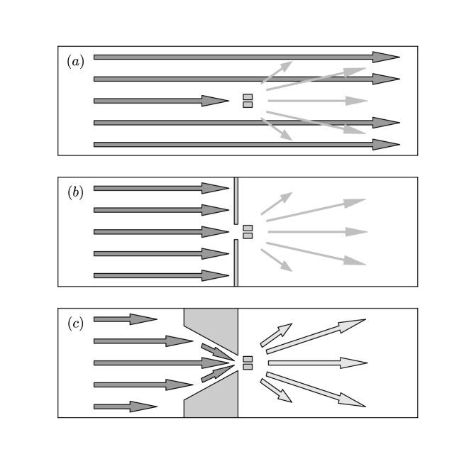
A schematic of an experiment conducted on a single antenna is shown in figure 1(a). A linearly polarized THz beam is used to illuminate a single plasmonic antenna. Since the antenna has an extinction cross section much smaller than the size of the beam, only a small fraction of the incident field is extinct by scattering and absorption in the antenna. The majority of the field is transmitted as unperturbed by the antenna, leading to a large background in extinction measurements. In order to reduce this background, a thin metallic screen can be used to only transmit the relevant part of the THz beam that interacts with the antenna (figure 1(b)). Although the signal-to-background ratio is improved in this configuration, only a small fraction of the pulse is used and the signal-to-noise is not increased. To enhance the signal-to-noise, it is possible to use a tapered waveguide. The conical design guides the off-center parts of the field in the direction of the antenna, resulting in an enhanced THz electromagnetic field at the output aperture. This field enhancement leads also to the enhanced response of the antenna, allowing a more sensitive spectroscopy.
The article is organized as follows: The fabrication of the bowtie antenna and the waveguides is described in section 2. In section 3, we present simulations of the near field enhancement of a single bowtie antenna and the conical waveguide, as well as its enhanced transmission. THz extinction measurements of a THz antenna at the output of the conical waveguide are compared with the extinction of a random array of similar antennas in section 4. These measurements demonstrate the enhanced extinction of single antennas mediated by the enhanced field at the output of the waveguide. The article is ended with the conclusions.
2 Waveguide and antenna fabrication
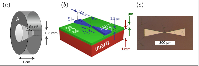
Two waveguides have been fabricated for the experiments. A conical shape waveguide is used to enhance the field at its output aperture and a cylindrical waveguide with the same output dimensions is used to reference the transmittance. The waveguides have been fabricated using electrical discharge machining: A conically tapered electrode with a half-angle of or a cylindrical electrode with diameter of are lowered through an aluminium plate, eroding a conical or cylindrical hole. The dimensions of the conically tapered waveguide are a thickness of , an output aperture with a diameter of and a half-angle of . The thickness of the cylindrical waveguide is and its diameter is . A schematic representation of the conical waveguide is shown in figure 2(a).
The semiconductor plasmonic antennas have been fabricated using conventional micro-fabrication techniques [17]: A silicon-on-insulator (SOI) wafer with a thick undoped top layer is implanted with arsenic atoms, introducing a free carrier concentration of . This doping level makes silicon a conductor at terahertz frequencies. The SOI wafer is bonded onto a thick quartz substrate with benzocyclobutene (BCB). The silicon substrate and oxide layer are subsequentially removed with wet chemical etching using KOH and HF. The antenna structures are defined using optical lithography and reactive ion etching.
The behavior of semiconductor antennas is determined by the doping level, and the antenna geometry. The bowtie antenna is formed by two monomers with a triangular shape with a base of , a triangle height of and monomer height of . The triangles have facing apexes, separated by a gap of . As it is shown below, this structure has a LSPR around . A schematic representation of the bowtie antenna and an optical microscope image are shown in figures 2(b) and 2(c), respectively. The cracks observed in the image are cracks in the BCB layer. These cracks have a typical width of a micron, being much smaller than the wavelength of THz radiation, and do not influence the measurements.
3 Simulations
The local field enhancement of the bowtie antenna and the transmission properties of the conical waveguide are studied using a 3D finite element method (FEM) in the frequency domain (COMSOL Multiphysics). For the simulations, we use the antenna dimensions determined from the optical image (figure 2(c)). The dielectric constant of n-doped Si at 0.4 THz is determined with the Drude model [18, 19] to be . For simplicity, we consider the antenna to be in vacuum and illuminated with a monochromatic continuous plane wave at normal incidence to the plane of the antenna. The frequency of the simulations is . As it is shown in section 4, the bowtie antenna has a LSPR around this frequency.
Figures 3(a) and 3(b) show the intensity enhancement of the electric field in the plane at the middle height of the antenna, normalized by the incident field. Figure 3(a) displays the intensity enhancement for a polarization of the incident wave along the long axis of the antenna, while figure 3(b) shows the intensity enhancement for a polarization along the short axis. Cuts through the intensity enhancement images along the long axis (horizontal-dashed lines) are shown in Figure 3(c), while cuts along short axis (vertical-dashed lines) are shown in Figure 3(d). The blue-solid and green-dashed curves represent the intensity enhancement for the polarization along the long axis and short axis, respectively.
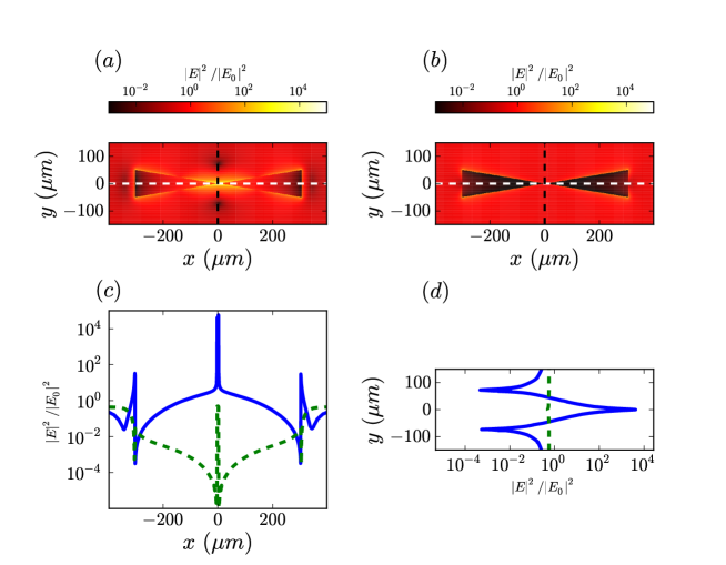
When driven along the long axis, the free electrons in the semiconductor bowtie antenna resonate at the LSPR frequency. There is a capacitive coupling of the two monomers across the gap. This coupling, arising from the coulomb attraction of charges across the short distance separating the two monomers, gives rise to an intensity enhancement in the gap. The enhancement is further increased by the lighting-rod effect that results from the sharp tips forming the apex of the triangles. The simulations show an intensity enhancement in the gap over 4 orders of magnitude. Note that this enhancement might be different in a real sample due to rounding of the antenna tips and the presence of the substrate. Nevertheless, the simulations illustrate that resonant bowtie antennas are capable of focusing and enhancing locally electromagnetic fields in subwavelength volumes. For an incident polarization along the short axis of the antenna there is no field enhancement relative to the incident field at . For this frequency and polarization the antenna is not resonant with the incident THz wave.
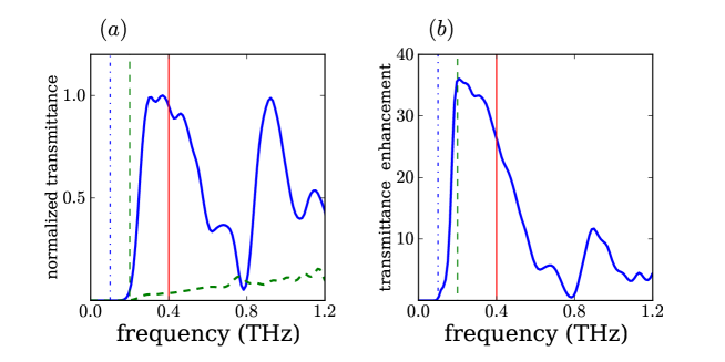
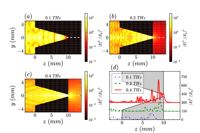
The transmission properties of the conically tapered and cylindrical waveguides are simulated using FEM and finite-difference in time domain (FDTD, CST Microwave Studio) techniques. As sketched in figure 1, a linearly polarized plane wave travels from left to right through the system. The dimensions of the waveguides used for the simulations are those described in section 3. The aluminium forming the waveguides is simulated as a perfect electric conductor. For the FDTD simulations a broadband Gaussian pulse is sent through the system, and the intensity of the transmitted field is monitored behind the waveguide, at a distance of after the output exit. The transmission spectra are obtained by Fourier transforming these fields. Figure 4(a) shows the transmittance spectrum, defined as the transmitted intensity normalized by the incident intensity, of the conically tapered waveguide with a blue-solid curve and of the cylindrical waveguide with a green-dashed curve. Both simulations have been normalized to the maximum transmittance of the conical waveguide at . At low frequencies the transmittance vanishes. These frequencies are below the cutoff frequency defined by the output aperture of the waveguides. For an infinitely long cylindrical waveguide with a diameter of the cutoff frequency is [20]. Below cutoff the wave entering the waveguide becomes evanescent. For a waveguide of finite length, the evanescent field can still be transmitted for frequencies just below cutoff.
Figure 4(b) shows the transmittance enhancement, which is defined as the transmittance through the conically tapered waveguide normalized by the transmittance through the cylindrical waveguide. The conically tapered waveguide enhances the transmitted field with respect to the cylindrical waveguide. While the cylindrical waveguide only transmits the fraction of the field incident onto the opening and reflects the rest, the conically tapered waveguide guides the incident field at the larger input aperture towards the smaller output aperture. These fields travel a longer distance, picking up an additional phase compared to the direct transmitted fields. For the given waveguide dimensions this results in destructive interference and a minimum in transmittance around . The entrance aperture of the conically tapered waveguide has a radius of , which is ten times the radius of the exit aperture. The 100 times larger energy illuminating the conically tapered waveguide compared to the cylindrical waveguide results in a maximum transmittance enhancement of around 35.
Figure 5 shows FEM simulations for the total field intensity enhancement in the conically tapered waveguide. A monochromatic and linearly y-polarized plane wave propagates from left to right. The total field enhancement in the plane through the center of the waveguide along the polarization direction -the yz plane- is shown for frequencies below 5(a), around 5(b) and above 5(c) cutoff. Cuts through these maps along the dashed white lines are shown in figure 5(d). For frequencies below cutoff there is an enhancement of the field inside the waveguide, but the transmission is reduced because the propagating field is fully reflected before the aperture is reached. The interference pattern in the intensity enhancement is the result of the interference of the incident field and this reflection. For waves having frequencies close to the cutoff frequency, there is a transition from the evanescent transmitted field to propagating waves. Figure 5(b) shows that although most of the wave is reflected a small fraction is transmitted. For frequencies well above cutoff, figure 5(c), the field propagates through the waveguide. This condition is needed for a maximum enhancement of the transmission. We note that even for this frequency, significant reflection takes place and the interference pattern is formed. This reflection can be minimized by reducing the tapering angle of the waveguide in order to allow an adiabatic focusing of the incident THz field onto the output aperture [10].
4 THz transmission and extinction measurements
The THz transmission experiments were carried out with a standard THz-TDS setup [3], in which a Ti:Sapphire oscillator (Femtolasers, Fusion 20-800), providing a train of pulses around , is used to generate broadband and linearly polarized THz pulses in a GaAs photoconductive antenna. The detection is done with a ZnTe crystal using the electro-optic effect. The THz beam has a Gaussian beam profile with a full width at half maximum of . The waveguide is placed in the THz beam, and the quartz substrate with the antenna is clamped in front of the waveguide.
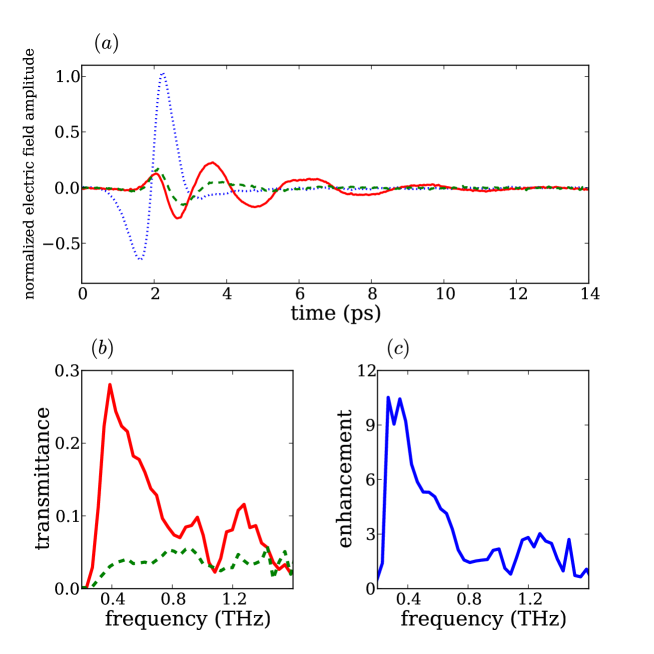
The experimental characterisation of the conically tapered and cylindrical waveguides is shown in figure 6. Both waveguides are measured in transmission and compared against each other and a reference measurement taken without waveguide, i.e., the response function of the setup. The time domain signals (figure 6(a)) show that the presence of the cylindrical waveguide severely reduces the transmitted signal, since most of the incident amplitude is blocked by the waveguide. The enhanced transmission of the conically tapered waveguide, relative to the cylindrical waveguide, is visible as an increase in the THz pulse dispersion. This is the contribution of the field that illuminated the entrance of the waveguide at a larger radius, and has picked up an additional phase before reaching the output aperture.
The transmittance spectra for the conically tapered (red-solid curve) and cylindrical (green-dashed curve) waveguides in figure 6(b) are obtained by Fourier transforming the time domain signals to obtain the power spectrum, and are normalized against the setup response, i.e., the power spectrum measured without any waveguide. For both waveguides the transmittance vanishes at the lowest frequencies due to cutoff. The transmittance remains below 0.05 for the cylindrical waveguide even at higher frequencies. This reduced transmittance is due to the large area of the incident beam that is blocked. In our setup, roughly 95 % of the energy carried by the THz beam is contained in an area of , while the area of the aperture of the cylindrical waveguide is . This ratio of 1/25 matches the experimental results. The transmittance is enhanced for the conical waveguide, compared to the cylindrical one. Most of the characteristics from the simulations shown in figure 4 are reproduced by the measurements. The transmittance approaches 0.3 at , while the output aperture only encloses around 5 % of the area of the incident pulse. The reduced transmittance around is also consistent with the simulations, and can be explained by the aforementioned destructive interference in the wavefront. The blue shift of this minimum in the measurements, compared to the simulations, can be attributed to the approximation of plane wave illumination used for the simulations. In the simulations, the complete input aperture is illuminated by a plane wave, whereas in the experiments the pulse has a Gaussian profile and it is slightly smaller than the input aperture of the waveguide. This smaller size of the beam reduces the effective height of the waveguide and introduces a blue-shift of the interference features. Figure 6(c) displays the transmittance of the conically tapered waveguide normalized by the cylindrical waveguide, showing the enhancement of the transmittance of the conically tapered waveguide over the complete range of . The maximum intensity enhancement is around one order of magnitude at .
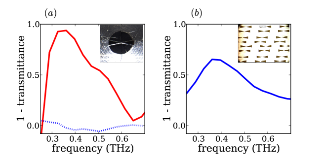
A single bowtie antenna is placed at the output aperture of the conically tapered waveguide, as shown in the inset of figure 7(a). The measured extinction, which is defined as 1 minus the transmittance, of this single antenna in front of the waveguide is shown in figure 7(a) with the solid-red curve. The transmission measurements through the single antenna are referenced to the transmission of the waveguide with an empty quartz substrate at the output entrance, i.e., without the antenna. A resonance is clearly resolved in this measurement with a maximum extinction of 90 % around . This enhanced extinction corresponds to the excitation of a LSPR in the plasmonic antenna, which should lead to a large local field enhancement in the bowtie gap. The blue-dashed curve in figure 7(a) corresponds to the extinction of the single antenna measured without the waveguide. The response is practically flat and the LSPR cannot be resolved.
To rule out any possible artifact in the measurements that could lead to an extinction peak similar to our measurements, we have confirmed the resonant response of the bowtie antenna by measuring the extinction of a random array of similar antennas without the conically tapered waveguide. An optical microscope image of the sample is shown in the inset of figure 7(b). In this measurement, the THz beam illuminates approximately 30 antennas. Therefore, the extinction is enhanced in this sample by increasing the density of antennas, rather than by concentrating the THz beam with the conical waveguide. A similar extinction spectrum to the single antenna is measured for the random array (figure 7(b)). The extinction reaches a maximum at 0.4 THz, with a resonant response that can be attributed to the excitation of LSPRs.
The demonstration of the enhanced extinction by a single bowtie antenna opens a range of possibilities for THz spectroscopy of nanostructures or of molecules at low concentrations. For example, the positioning of a nanostructure in the subwavelength gap defined by the two monomers, in which the field is locally enhanced, will enable to increase the THz field-matter interaction to a level at which far-field spectroscopy of single nanostructures at THz frequencies might be possible.
5 Conclusion
We have experimentally demonstrated that a conically tapered waveguide can be used to funnel and enhance the THz intensity. This intensity enhancement allows us to measure the extinction of a single THz plasmonic bowtie antenna, which otherwise cannot be detected due to the large background of unscattered radiation. The transmittance properties are also investigated numerically finding an excellent agreement with the measurements. The large localized field enhancements that can be achieved by bowtie antennas in subwavelength volumes, may open the possibility of using standard far-field THz time domain spectrometers for the detection and spectroscopy of single nanostructures.
References
References
- [1] Ferguson B and Zhang X C 2002 Materials for terahertz science and technology Nature Materials 1 26-32
- [2] Tonouchi M 2007 Cutting-edge terahertz technology Nature Photonics 1 97-105
- [3] Dexheimer S L (ed) 2008 Terahertz Spectroscopy: Principles and Applications (Optical Science and Engineering series) (CRC Press)
- [4] Jepsen P U, Cooke D G and Koch M 2011 Terahertz spectroscopy and imaging - Modern techniques and applications Laser Phot. Rev. 5 124-66
- [5] Shi X, Cleary A, Khalid A and Cumming D R S 2009 Multiple plasmon resonances at terahertz frequencies from arrays of arsenic doped silicon dots Microelec. Eng. 86 1111-3
- [6] Tian Z, Azad A K, Lu X, Gu J, Han J, Xing Q, Taylor A J, O’Hara J F and Zhang W 2010 Large dynamic resonance transition between surface plasmon and localized surface plasmon modes Opt. Express 18 12482-8
- [7] Berrier A, Ulbricht R, Bonn M and Gómez Rivas J 2010 Ultrafast active control of localized surface plasmon resonances in silicon bowtie antennas Opt. Express 18 23226-35
- [8] Giannini V, Berrier A, Maier S A, Sanchez-Gil J A and Gómez Rivas J 2010 Scattering efficiency and near field enhancement of active semiconductor plasmonic antennas at terahertz frequencies Opt. Express 18 2797-807
- [9] Saxler J, Gómez Rivas J, Janke C, Pellemans H P M, Haring Bolivar P and Kurz H 2004 Time-domain measurements of surface plasmon polaritons in the terahertz frequency range Phys. Rev.B 69 155427
- [10] Rusina A, Durach M, Nelson K A and Stockman M I 2008 Nanoconcentration of terahertz radiation in plasmonic waveguides Opt. Express 23 18576-89
- [11] Kim S-H, Lee E S, Ji Y B and Jeon T I 2010 Improvement of THz coupling using a tapered parallel-plate waveguide Opt. Express 18 1289-1295
- [12] Zon V B and Zon B A 2011 Terahertz surface plasmon polaritons on a conductive right circular cone: Analytical description and experimental verification Phys. Rev.A 84 013816
- [13] Zhang J and Grischkowsky H 2005 Adiabatic compression of parallel-plate metal waveguides for sensitivity enhancement of waveguide THz time-domain spectroscopy Appl. Phys. Lett. 86 061109
- [14] Zhan H, Mendis R and Mittleman D M 2010 Superfocusing terahertz waves below using plasmonic parallel-plate waveguides Opt. Express 18 9643-50
- [15] Wächter M, Nagel M and Kurz H 2009 Tapered photoconductive terahertz field probe tip with subwavelength spatial resolution Appl. Phys. Lett. 95 041112
- [16] Nguyen T D, Vardeny Z V and Nahata A 2010 Concentration of terahertz radiation through a conically tapered aperture Opt. Express 18 25441-8
- [17] Berrier A, Albella P, Ameen Poyli M, Ulbricht R, Bonn M, Aizpurua J and Gómez Rivas J 2012 Detection of deep-subwavelength dielectric layers at terahertz frequencies using semiconductor plasmonic resonators Opt. Express 20 5052-60
- [18] Ashcroft N W and Mermin N D 1976 Solid State Physics (Saunders)
- [19] Adachi S 2004 Handbook on physical properties of semiconductors vol 1 (Boston, Kluwer)
- [20] Marcovitz N 1964Waveguide Handbook (Lexington, MA: Boston Technical Publishers)