Why is the bulk resistivity of topological insulators so small?
Abstract
As-grown topological insulators (TIs) are typically heavily-doped -type crystals. Compensation by acceptors is used to move the Fermi level to the middle of the band gap, but even then TIs have a frustratingly small bulk resistivity. We show that this small resistivity is the result of band bending by poorly screened fluctuations in the random Coulomb potential. Using numerical simulations of a completely compensated TI, we find that the bulk resistivity has an activation energy of just times the band gap, in good agreement with experimental data. At lower temperatures activated transport crosses over to variable range hopping with a relatively large localization length.
The three-dimensional (3D) topological insulator (TI) Fu et al. (2007); Moore and Balents (2007); Roy (2009); Fu and Kane (2007); Qi et al. (2008) has gapless surface states that are expected to exhibit a range of interesting quantum phenomena Hasan and Kane (2010); Qi and Zhang (2011). While a number of 3D TIs have been identified, most of these are poor insulators in the bulk, so that the properties of the surface are obscured in transport measurements. For this reason achieving a bulk-insulating state remains an active topic of research Qu et al. (2010); Analytis et al. (2010a); Xiong2012hsh; Checkelsky et al. (2009); Butch et al. (2010); Analytis et al. (2010b); Eto et al. (2010); Ren et al. (2011a, b, 2012).
Typically, as-grown TI crystals are heavily doped -type semiconductors, and correspondingly they exhibit metallic conduction. In order to make them insulating these TIs are compensated by acceptors. With increasing compensation , where and are the concentrations of monovalent donors and acceptors, repsectively, the Fermi level shifts from the conduction band to inside the band gap and then at into the valence band. When compensation of donors is complete, , the Fermi level is in the middle of the gap and the most insulating state of the TI is reached. The hope is that at the bulk resistivity should obey the activation law,
| (1) |
with an activation energy that is equal to half the band gap . Here, is a constant and is the thermal energy. Since typically eV, this expectation would imply a well-insulating bulk at room temperatures and below.
The typical experimental situation at , however, is frustrating Ren et al. (2011b). In the range of temperatures between and K the resistivity is activated, but with an activation energy that is three times smaller than expected, meV. At K the activated transport is replaced by variable range hopping (VRH), characterized by with , and the resistivity grows even more slowly with decreasing . In Ref. Ren et al., 2011b the authors show that Mott VRH () provides a reasonable fit to their data at K K. Definite characterization of the temperature exponent is difficult, however, due to the relatively narrow window of temperature and to variations between samples. At K the resistivity saturates due to the contribution of the surface states.
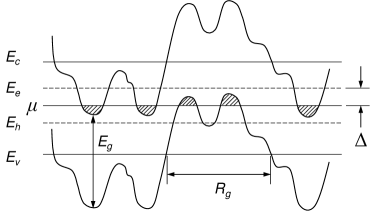
In this paper we suggest an explanation for the unexpectedly small bulk resistivity of TIs. We assume that both donors and acceptors are shallow and we use the theory of completely compensated semiconductors (CCS) Shklovskii and Efros (1972); Efros and Shklovskii (1984). This theory is based on the idea that near , when almost all donors and acceptors are charged, random fluctuations in the local concentration of impurities result in large fluctuations of charge. The resulting Coulomb potential is poorly screened because of the vanishing average concentration of screening electrons. Huge fluctuations in the random potential bend the conduction and valence bands edges and in some places bring them to the Fermi level, thereby creating electron and hole puddles that non-linearly screen the random potential. Thus, the amplitude of fluctuations is limited only by the semiconductor gap . As a result the ground state of a CCS, shown in Fig. 1, is similar to a network of - junctions Shklovskii and Efros (1972); Efros and Shklovskii (1984). The characteristic size of these - junctions, also called the nonlinear screening radius, is given by
| (2) |
where is the dielectric constant, is the electron charge, and . For cm-3 and , nm nm, so that we deal with a very long range potential. As a result, the resistivity can be dramatically different from the expectation outlined above, which assumed flat bands. First, at relatively high temperatures conduction is due to electrons and holes being activated from the Fermi level to their corresponding classical percolation levels (classical mobility edges), and , in the conduction and the valence bands. These may be substantially closer to the Fermi level than , but so far the resulting value of has not been studied theoretically. Second, at sufficiently low temperatures electrons and holes can hop (tunnel) between distant puddles, so that variable range hopping replaces activated transport. In the low temperature limit should obey the Efros-Shklovskii (ES) law of VRH Efros and Shklovskii (1975),
| (3) |
where , is the localization length of states with energy close to the Fermi level, and is a numerical coefficient. So far the magnitude of and the nature of the crossover between activated and VRH conduction have not been studied.
In this paper, motivated by the TI resistivity puzzle, we return to CCS and model numerically the case. For moderately large we find that . For a TI with eV this implies meV, in agreement with observed values Ren et al. (2011b). We also calculate the single-particle density of states (DOS) of impurity states, and we find that the DOS has a Coulomb gap at the Fermi level Efros and Shklovskii (1975). We show from our simulation that the resistivity is described by Eq. (3) at low temperatures and crosses over to Eq. (1) at higher . We present a crude estimate of the localization length which suggests that K and that the crossover between activation and ES VRH occurs at K. Together our results for the activated and VRH resistivity establish a universal upper limit for the resistivity that one can achieve for a 3D TI compensated by shallow inpurities.
In order to model the CCS numerically, we simulate a cube filled by an equal number of randomly positioned donors and acceptors (20000 of each). We numerate all donors and acceptors by the index and we define as the number of electrons residing at impurity and the variable to discriminate between donors () and acceptors (). The resulting Hamiltonian is
| (4) |
where is the net charge of site and all energies are defined relative to the middle of the band gap. The first term of Eq. (4) contains the energies of donor and acceptor sites, which for the case of shallow impurities is very close to . The second term is the total interaction energy of charged impurities. For two impurities at a distance , where is the Bohr radius of impurity states, one can describe their interaction using the normal Coulomb law . For example, an empty donor shifts the energy of an electron at a distant filled donor by an amount . On the other hand, for a pair of impurities with separation , quantum mechanical averaging over the electron wavefunction becomes important (such close impurity pairs are common in heavily doped semiconductors, where ). A pair of very close donors, for example, cannot create an electron state deeper than that of the helium-like ion with binding energy . In order to capture this quantum phenomenon in an approximate way, we use the classical Hamiltonian of Eq. (4) with a truncated Coulomb potential . The result of this truncation is to eliminate the unphysically deep electron states that would result from very compact impurity pairs with an unmodified interaction. We will show below that our results are mostly insensitive to the details of this truncation. Note that Eq. (4) does not include the kinetic energy of electrons and holes in the conduction and valence bands and, therefore, aims only at describing the low temperature () physics of CCS.
In all results below we use dimensionless units for , , , , , and , measuring all distances in units of and all energies in units of . Thus, Eq. (4) can be understood as dimensionless, with and . For a TI with eV, and cm-3, the unit of energy meV, so that the dimensionless gap . We were unable to directly model , since in this case the very large leads to large size effects. Instead, we present results for the more modest , where and size effects are negligible, and for , where and size effects can be treated using extrapolation. Unless otherwise stated, results below use and are averaged over random initializations of the donor and acceptor positions.
In our simulation, we first search for the set of electron occupation numbers that minimizes . We start by assuming that all donors are empty (, ) and that all acceptors are filled (, ). These charged donors and acceptors create a random Coulomb potential whose magnitude exceeds . We then sequentially choose pairs consisting of one filled site and one empty site and attempt to transfer an electron from the filled site to the empty site. If the proposed move lowers the total system energy , it is accepted, otherwise it is rejected. To describe the change in resulting from such a transfer it is convenient to introduce the single-electron energy state, , at a given impurity :
| (5) |
The process of transferring electrons concludes when all pairs with and satisfy the ES stability criterion:
| (6) |
This final arrangement of electrons can be called a pseudo-ground state, since higher stability criteria of the ground state (involving multiple simultaneous electron transfers) are not checked. Such pseudo-ground states are known to accurately describe the properties of the real ground state at all but extremely small energies Efros and Shklovskii (1984); Möbius et al. (1992); Efros et al. (2011).
Once the pseudo-ground state is known, the DOS is calculated by making a histogram of the single-electron energies . The result is shown in Fig. 2, with the DOS in units of , so that the total area is equal to unity. Occupied and empty states are separated by the Fermi level at . The nearly constant DOS between to reflects a practically uniform distribution of the random potential from to . Near the Fermi level one sees the Coulomb gap that is a universal result of the ES stability criterion Efros and Shklovskii (1975).

Once the energies are calculated, we evaluate the resistivity using the approach of the Miller-Abrahams resistor network Efros and Shklovskii (1984). Namely, each pair of impurities is said to be connected by the resistance , where the activation energy is defined Efros and Shklovskii (1984) as follows:
| (7) |
The resistivity of the system as a whole is found using a percolation approach. Specifically, we find the minimum value such that if all resistances with are left intact, while others are eliminated (replaced with ), then there exists a percolation pathway connecting opposite faces of the simulation volume. The system resistivity is taken to be proportional to , which captures the exponential term while details of the prefactor are ignored Efros and Shklovskii (1984).
In Fig. 3 we plot the computed resistivity as a function of temperature, using the dimensionless logarithm of the resistance and the dimensionless temperature . These notations are introduced to exclude any explicit dependence on . Fig. 3(a) shows versus over the huge range of temperatures . One can see that at low temperatures the resistivity is well described by the ES law, Eq. (3), with . The higher temperature range is plotted separately as a function of in Fig. 3(b). Here we find two activated regimes of hopping conductivity. At extremely high temperatures we see the large activation energy while in the intermediate range we see an activation energy . We repeated this analysis for the larger band gap using systems of 10000, 20000 and 30000 donors and by extrapolating to infinite size we find . These results for remain unchanged, within our statistical uncertainty, if we use instead of .
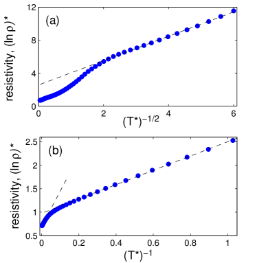
It should be noted that the large activation energy observed at does not have any physical meaning for a real CCS, since at such large temperatures the conduction is not due to hopping but rather to free, “hot” carriers far from the conduction and valence band edges. Nonetheless, for our model Hamiltonian this result is consistent with established theories which say that at such large temperatures , where denotes averaging over all pairs (see Ch. 8 of Ref. Efros and Shklovskii, 1984).
On the other hand, the second activation energy makes full physics sense and should be seen in experiment. At electrons optimize their conductivity by hopping among impurities that are energetically close to the Fermi level. The activation energy can be understood as the resulting percolation level for hopping between nearest-neighboring sites. In other words, if electrons are activated only to those sites with , then precisely at there exists an infinite conduction pathway for electrons comprised of hops of length or shorter. In a heavily doped semiconductor this energy is equivalent to the activation energy of electrons from the Fermi level to the conduction band mobility edge . (Of course, holes are activated from the Fermi level to their percolation level as well.) For a typical TI eV, so that we get meV, in good agreement with typical experimental data Ren et al. (2011b). (We note, however, that recent experiments on Sn-doped Bi2Te2Se have achieved meV Ren et al. (2012). Such large activation energies may be associated with deep donor impurity levels, which go beyond our model.)
This activation to the percolation level persists until much smaller temperatures, where becomes prohibitively large compared to the thermal energy. At such small conduction proceeds by VRH among electron/hole puddles at the Fermi level and the resistivity is given by Eq. (3).
One can interpret the relatively small numerical factor above by recalling that in a typical 3D continuous random potential, of space has a potential smaller than the percolation level Efros and Shklovskii (1984). As we demonstrated above the energy of the conduction band bottom is roughly uniformly distributed in the interval . This means that the percolation level should be close to and makes our result quite reasonable.
So far we have emphasized results that do not explicitly depend on the localization length . In fact, knowledge of is necessary to predict and the transition temperature between Eq. (1) and Eq. (3) in real temperature units. (According to Fig. 3a, the transition happens at , or ). We argue now that in a TI is quite large, leading to a prominent role for VRH. To see this, consider that if an electron with energy close to the Fermi level is assumed to tunnel from one electron puddle to another distant puddle along the straight line connecting them, then the tunneling path passes through regions where the conduction band bottom is quite high above Fermi level. This implies a small tunneling amplitude, or . In fact, however, a tunneling electron can use the same geometrical path as a classical percolating electron with energy above the Fermi level. In order to roughly estimate , we assume that along such a classical percolation path the tunneling barriers are uniformly distributed in the range and we neglect the curvature of this path. Integrating the action along this path then gives . For a TI with and this gives . This crude estimate leads to K and K, which is similar in magnitude to the experimentally observed K where the resistivity crosses over from activated to VRH behavior Ren et al. (2011b).
We note that if one plots our result for against in the relatively narrow crossover range K K, one gets a mostly straight line, as seen in Ref. Ren et al., 2011b. However, our results suggest that at low temperatures the bulk resistivity follows the ES law of VRH with temperature exponent , which should become apparent if the bulk resistivity can be probed to very low temperature. Such measurements are presumably possible in samples that are much thicker than those studied in Ref. Ren et al., 2011b ( m). For such thick samples conduction through the bulk of the TI crystal dominates over the surface transport until much smaller temperatures.
To conclude, we have studied numerically the bulk resistivity of a TI crystal with band gap as a CCS. We find that at high temperatures the resistivity is activated with relatively small activation energy , in agreement with experimental data Ren et al. (2011b). At lower temperatures the resistivity crosses over to ES VRH, with an estimated characteristic temperature K. Thus, Eq. (3) with K at K and Eq. (1) with at K give the upper limit for resistivity that one can achieve for a heavily doped and completely compensated TI with shallow impurities.
We are grateful to Y. Ando, A. L. Efros, M. S. Fuhrer, Yu. M. Galperin, M. Müller, and N. P. Ong for useful discussions. This work was supported primarily by the MRSEC Program of the National Science Foundation under Award Number DMR-0819885. T. Chen was partially supported by the FTPI.
References
- Fu et al. (2007) L. Fu, C. L. Kane, and E. J. Mele, Phys. Rev. Lett. 98, 106803 (2007).
- Moore and Balents (2007) J. E. Moore and L. Balents, Phys. Rev. B 75, 121306 (2007).
- Roy (2009) R. Roy, Phys. Rev. B 79, 195322 (2009).
- Fu and Kane (2007) L. Fu and C. L. Kane, Phys. Rev. B 76, 045302 (2007).
- Qi et al. (2008) X.-L. Qi, T. L. Hughes, and S.-C. Zhang, Phys. Rev. B 78, 195424 (2008).
- Hasan and Kane (2010) M. Z. Hasan and C. L. Kane, Rev. Mod. Phys. 82, 3045 (2010).
- Qi and Zhang (2011) X.-L. Qi and S.-C. Zhang, Rev. Mod. Phys. 83, 1057 (2011).
- Qu et al. (2010) D.-X. Qu, Y. S. Hor, J. Xiong, R. J. Cava, and N. P. Ong, Science 329, 821 (2010).
- Analytis et al. (2010a) J. G. Analytis, R. D. McDonald, S. C. Riggs, J.-H. Chu, G. S. Boebinger, and I. R. Fisher, Nat. Phys. 6, 960 (2010a).
- Checkelsky et al. (2009) J. G. Checkelsky, Y. S. Hor, M.-H. Liu, D.-X. Qu, R. J. Cava, and N. P. Ong, Phys. Rev. Lett. 103, 246601 (2009).
- Butch et al. (2010) N. P. Butch, K. Kirshenbaum, P. Syers, A. B. Sushkov, G. S. Jenkins, H. D. Drew, and J. Paglione, Phys. Rev. B 81, 241301 (2010).
- Analytis et al. (2010b) J. G. Analytis, J.-H. Chu, Y. Chen, F. Corredor, R. D. McDonald, Z. X. Shen, and I. R. Fisher, Phys. Rev. B 81, 205407 (2010b).
- Eto et al. (2010) K. Eto, Z. Ren, A. A. Taskin, K. Segawa, and Y. Ando, Phys. Rev. B 81, 195309 (2010).
- Ren et al. (2011a) Z. Ren, A. A. Taskin, S. Sasaki, K. Segawa, and Y. Ando, Phys. Rev. B 84, 075316 (2011a).
- Ren et al. (2011b) Z. Ren, A. A. Taskin, S. Sasaki, K. Segawa, and Y. Ando, Phys. Rev. B 84, 165311 (2011b).
- Ren et al. (2012) Z. Ren, A. A. Taskin, S. Sasaki, K. Segawa, and Y. Ando, Phys. Rev. B 85, 155301 (2012).
- Shklovskii and Efros (1972) B. I. Shklovskii and A. L. Efros, Sov. Phys.-JETP 35, 610 (1972).
- Efros and Shklovskii (1984) A. L. Efros and B. I. Shklovskii, Electronic Properties of Doped Semiconductors (Springer-Verlag, New York, 1984) Available from http://www.tpi.umn.edu/shklovskii.
- Efros and Shklovskii (1975) A. L. Efros and B. I. Shklovskii, J. Phys. C: Solid State Phys. 8, L49 (1975).
- Möbius et al. (1992) A. Möbius, M. Richter, and B. Drittler, Phys. Rev. B 45, 11568 (1992).
- Efros et al. (2011) A. L. Efros, B. Skinner, and B. I. Shklovskii, Phys. Rev. B 84, 064204 (2011).
- Efros (1976) A. L. Efros, J. Phys. C: Solid State Phys. 9, 2021 (1976).