A Piggyback resistive Micromegas
Abstract
A novel read-out architecture has been developed for the Micromegas detector. The anode element is made of a resistive layer on a ceramic substrate. The detector part is entirely separated from the read-out element. Without significant loss, signals are transmitted by capacitive coupling to the read-out pads. The detector provides high gas gain, good energy resolution and the resistive layer assures spark protection to the electronics. This assembly could be combined with modern pixel array electronic ASICs. This readout organization is free on how the pixels are designed, arranged and connected. We present first results taken with a Medipix2 read-out chip.
keywords:
Micromegas; Piggyback; resistive; ceramic; detector1 Introduction
One of the most prominent problems associated with gas-filled proportional chambers is the sparking induced by heavily ionizing particles producing large deposits. Amplified by the avalanche process they could reach a critical charge density, related to the Raether’s limit [1], and could evolve into a discharge. As a result, a large fraction of the stored charge defining the amplification field is lost. The presence of discharges limits the high rate operation of the detector due to the required power supply recovery time, reduces the mean life of the detector and risks the damage of the readout electronics due to the high currents reached by these spark processes.
In Micromegas (MM) detector [2, 3] discharges are not destructive but they must be reduced in order to obtain a safe operation.
To avoid any damage of the electronics, most of the detectors are using an additional protecting circuit, which interfaces the readout strips or pads with the front-end electronics. Recently new developments are undertaken to further improve the spark protection to operate at higher rates. A first promising approach is employing a resistive foil on top of the anode plane [4]. When a streamer develops the increasing number of charges is deposited at the high resistivity foil. The anode potential generated by these charges reduces the amplification field, quenching the streamer resulting from field loss. A required condition is that the anode potential must last for a period of time long enough such that the charges present in the streamer have been completely evacuated, which introduces the need for high resistive values. The resistive foil limits the charge transfer, protecting the electronics, and avoids the total discharge of the mesh reducing the dead time of the detector.
Protection against discharges becomes mandatory in the case of GridPix detectors, where the Micromegas is placed directly on a pixelized silicon chip. The damage can be due to the plasma that locally melts or evaporates the chip material, or by a breakdown of electronic circuitry, due to too high potentials or charges. Even a local damage will not affect only a single channel, as it is the case in conventional read-out, but the whole chip will be damaged. Moreover, since the Micromegas is integrated in the chip, the whole structure must be replaced. In order to protect the chip from discharges a high-resistive layer of 5 m up to 25 m of amorphous silicon is deposited on the chip [5, 6].
For large Micromegas detectors, a novel protection scheme has been developed by a group working on hard radiation detectors at CERN [7, 9]. According to this scheme, we are using resistive strips above the readout electrode to overcome the spark problem. This is a quite efficient and robust solution for fabricating very-large area detectors.
We present a new approach called "Piggyback" resistive Micromegas where a thin resistive layer is deposited on an adequate insulator. This element is used as substrate for the Micromegas which could be fabricated for instance by using the "bulk" technology [10].
2 The new technology description
The new idea proposed consists in separating the detector part from the read-out part as shown in figure 1; the signal is transmitted by capacitive coupling to the read-out pads. The technology used here is inspired from a similar development on a Parallel Plate Avalanche Counter described in reference [11].
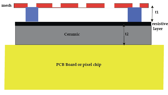
In the proposed technology the amplification gap (t1) is about 100 m and it is achieved between a woven stainless steel mesh connected to the high voltage and a resistive anode. In some special configurations the anode element could be also connected to high voltage. By adding a drift electrode, a MM detector operates as usually in the proportional avalanche mode inducing signals on the resistive anode plane. Various elements of the structure are optimized in such a way that the electronic signal is not lost through the resistive layer but is propagated to a separate plane, carrying read-out pads or strips, by capacitive coupling. A schematic view of the new structure is shown in figure 1 where we can see the various elements: the Micromegas structure with the pillars; the resistive layer; the ceramic substrate and the readout board. The read-out plane can be a simple PCB board or a pixel chip such as the Medipix2 [6] or any similar integrated chip. The thickness of the resistive layer is of the order of 10 m.
In order to optimize the induced signal by capacitive coupling the thickness of the insulator (t2) must be kept small to satisfy the relation
| (1) |
where is the dielectric constant of medium 1 (gas) and is the dielectric constant of medium 2 (insulator). Because the insulator plays at the same time the role of vessel of the detector the thickness should be kept reasonable (several hundred m). In order to satisfy 1 the material should have a dielectric constant as high as possible. Good candidates are ceramic insulators having large dielectric constants (10). In our first prototype we have used a standard amplification gap of t1=128 m, the ceramic insulator was alumina with t2=300 m (=10). The selection of the resistive layer is usually a challenge in gas detectors in order to find an appropriate resistivity and a good surface quality. The ruthenium oxide (RuO2) has been chosen. This latter is extensively used for coating ceramics at high temperature for the preparation of resistors or integrated circuits.
The RuO2 based thick film was prepared by a standard screen printing technique from a commercial paste having a resistivity of 100 M. This is a cost effective industrial process that permits to get a robust and stable layer with a variety of values for the resistivity: 1 M to hundreds of G. The combination of the ceramic insulator, having an excellent surface quality and the robustness of the resistive layer, provides a solid solution for our structure.
3 Experimental set-up and results
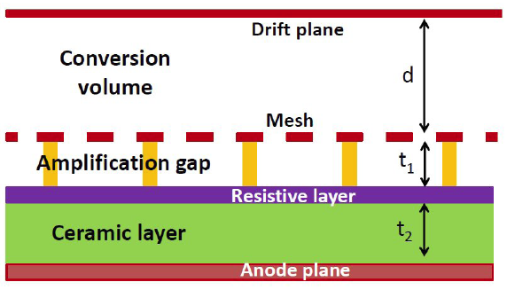
Three small detectors, with the schematic shown in figure 2, were fabricated for these tests. The ceramic substrate was made out of standard alumina of 300 m-thickness (t2). A 20 m thick RuO2 based film with a resistivity of 100 M was processed above it. The backside of the ceramic layer was covered by a copper layer, which acted as the anode plane, and a bulk Micromegas structure [10] was built on the resistive layer, with an amplification gap of 128 m (t1). The whole structure was situated inside a gas chamber, specifically designed for these tests, and a mesh frame was used as the drift plane, in order to define a 10 mm thick conversion volume.
From the three detectors built, only the number 1 and 3 worked during the tests. They were illuminated by a 55Fe source keeping a constant gas flow. The mesh voltage was varied from 300 to 450 V, the drift from 400 to 1200 V and the anode was connected to ground. Mesh and drift voltages were independently powered by a CAEN N471A module. The avalanche in the Micromegas structure induces a negative signal in the mesh and a positive one in the anode. Both signals were respectively monitored by two CANBERRA preamplifiers to evaluate their efficiency. The preamplifier outputs were fed into two CANBERRA 2006 amplifiers and subsequently into a multichannel analyzer AMPTEK MCA-8000A for spectra acquisition. Each spectrum was fitted by two Gaussian functions, corresponding to the Kα (5.9 keV) and Kβ (6.4 keV) lines of the 55Fe source; the mean position and width of the main peak were obtained for each fit.
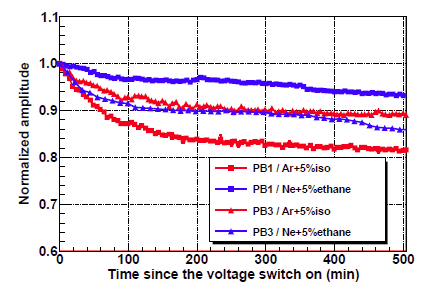
Two types of gas mixtures were used in these tests: Argon + 5% Isobutane (iC4H10) and Neon + 5% Ethane (C2H6). The voltage was then switched on and the evolution of the detector’s gain was studied generating an energy spectrum integrated for 1 minute every 5 minutes during several hours. As shown in figure 3, the gain of this type of detectors decreases during the first 100 minutes, until a stable operation point is reached. The gain may later change due to pressure and temperature variations, as the amplification gap of 128 m is not the optimum for the gas mixtures used [2].
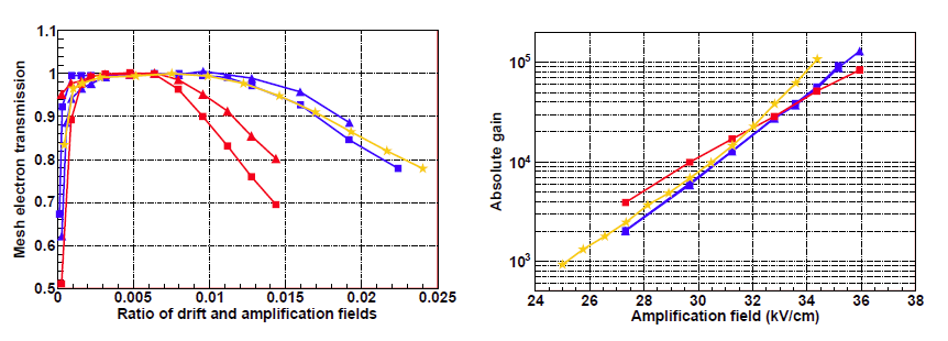
Once the gain has stabilized, the drift voltage was varied for a fixed mesh voltage to obtain the electron transmission curve, shown in figure 4 (left). As a typical Micromegas detector, these curves show a "plateau" of maximum electron transmission for a range of low drift fields. For more intense fields, the mesh stops being transparent for the primary electrons generated in the conversion volume and both the gain and the energy resolution degrade. The ratio of drift and amplification fields was then fixed to an optimum and the mesh voltage was varied. The dependence of the peak position with the mesh voltage generates the gain curve, shown in figure 4 (right). Both detectors showed slightly lower gains than a standard 128 m-thickness bulk detector for the same mesh voltages but they both reached values up to 105 before the spark limit.
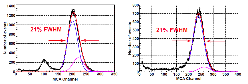
The energy resolution of both detectors was 21% (FWHM) at 5.9 keV in Ar+5%iC4H10 and in Ne+5%C2H6, as shown in figure 5. These values are slightly worse than for bulk detectors, which can reach values 16% (FWHM) at 5.9 keV in argon-isobutane mixtures, but discharges are highly suppressed.
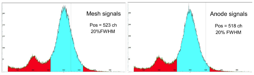
Finally, the signal induced both in the mesh and the anode plane was compared to evaluate possible losses at the anode plane by the thick ceramic layer. As shown in figure 6, the signal was entirely propagated to the induction plane and the energy spectrum of both the mesh and the anode planes showed similar values, with an efficiency better than 90%.
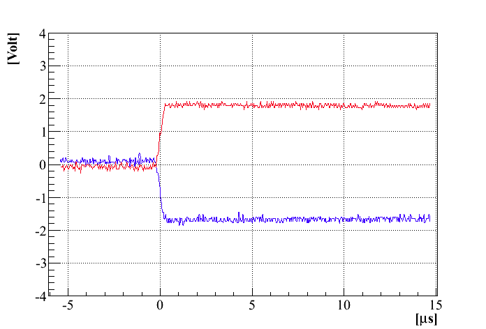
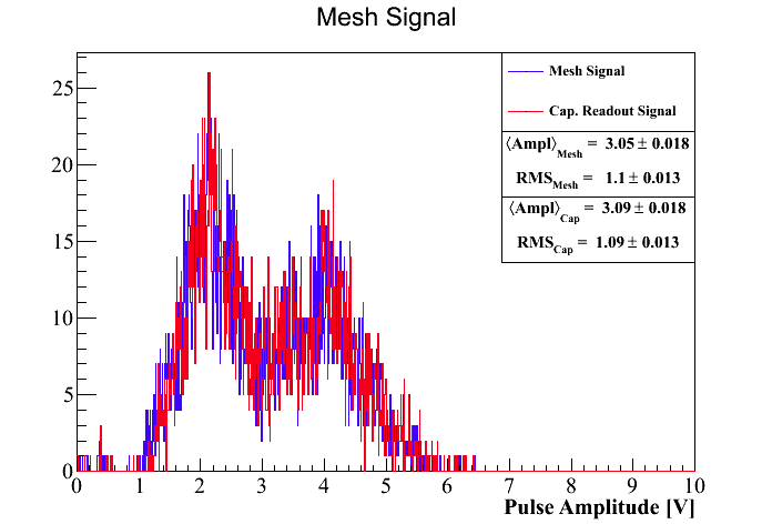
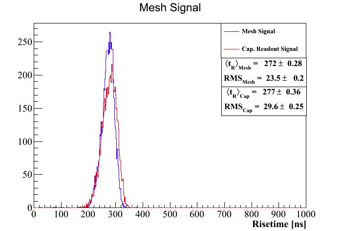
In order to minimize the -possibly- different behavior of the electronics chain to positive and negative signals, we repeated the measurement using a 252Cf source and two Ortec 142B preamplifiers registering the mesh and anode signals. The signals were registered simultaneously while the measurement was repeated after interchanging the preamplifiers to exclude systematics. The fission fragments deposit enough energy to create very big signals. Their range in the argon gas is of the order of 1 cm, so the rise time is expected to be of the order of 200-300 ns. A typical signal recorder simultaneously by the mesh and by the anode plane is shown on figure 7. At the same figure is also shown the accumulated signals from 5000 events.
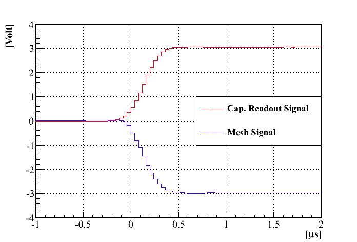
The amplitude and rise time distributions of the registered pulses are shown in figure 8. The response of the preamplifiers to negative and to positive signals was measured with the help of a pulse generator and was found to be the same within 5% (small loss for negative pulses). Given that fact and the results shown in figure 8, we verify that the signal loss due to the capacitance of the ceramic is less than 10%. The rise time of the pulses is also the same for both polarities within few percent, and does not appear to be affected by the resistive film, being within the expected range of 200-300 ns.
4 Rate capability
Additional tests were performed using an X-ray generator which allowed the illumination of the Piggyback structure at several rates. The structure was placed inside a chamber with a drift gap of 0.5 cm. The copper peak (8 keV) from the X-ray generator cathode was used during these measurements as a gain reference. Given that the minimum generator intensity was already high a foil of about 100 m Cu and some additional aluminum was used to attenuate the overall flux.
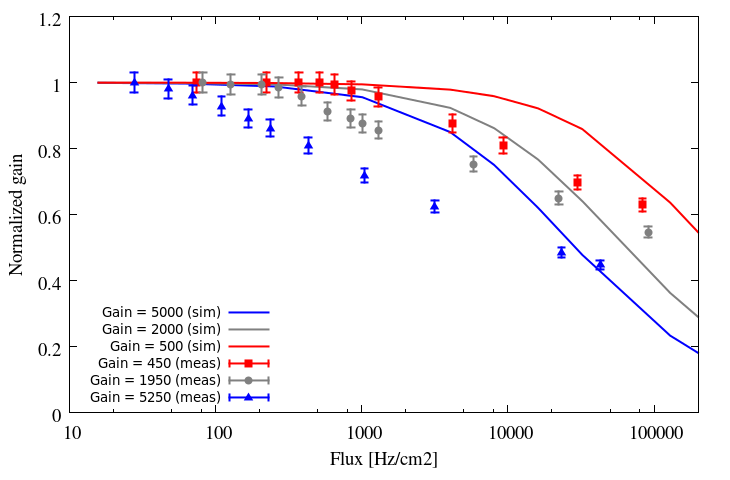
Gain measurements under the same conditions were done for different amplification gain values corresponding to different mesh voltages (440V, 500V and 530V) for X-ray fluxes up to about 100 kHz/cm2, as observed in figure 9.
These measurements show a "plateau" region dependent on the mesh voltage applied and that extends to higher fluxes for lower values of the amplification field. The gain stability was measured at low rates just after the system was started and the Piggyback illuminated with X-rays, showing gain stability better than 2%.
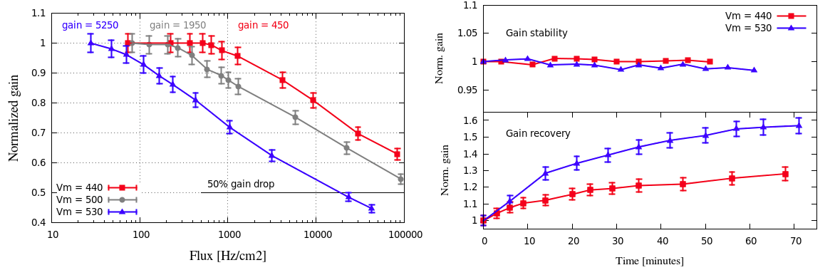
For higher rates, the gain drops as a function of the flux and the time required to achieve a stable gain is in the order of several minutes. The recovery time from the highest rates applied to the "plateau" region is shown also in figure 9.
It must be noticed that the gain dependency with the rate is not an intrinsic feature of the Piggyback structure and will also depend on the resistivity and effective ceramic capacitance chosen, allowing tuning up the values depending on the application, i.e. lower values of the resistivity would lead to an extended "plateau" for higher rates and enhanced gain stability at higher rates.
5 Simulation of charge diffusion effects over a resistive plate
Charge diffusion over the resistive top plane could be one of the main causes of the observed behavior of the Piggyback. In this section we show that the accumulation of charge over time due to slow charge diffusion in the illuminated region could be affecting the measured gain and be directly related to the stabilization time required. The charge diffusion relation for a given charge , which follows a Gaussian distribution of width , was provided in [8]
where the parameter it is related to the surface resistivity and surface capacitance . The accumulated charge will be translated into a surface potential given by the capacitance of the ceramic and thus, in a reduction of the amplification field. In order to study such reduction a narrow region around the Gaussian distributed charge has been chosen. The evolution on time of the total charge inside this region, defined by the radius , it is integrated from the previous expression and is described by the following relation
We can extrapolate this relation to the case of a continuous current flow by assuming this relation is valid for a differential element of charge. Integrating these differential contributions over time will allow us to calculate the accumulated charge at any time,
where we should take into account that these differential charge contributions will be related to the local amplification field, modified by the anode potential at the resistive plane at each time interval.
The integral will be calculated by adding the charge contributions at each time interval n, and describing the gain in terms of the relative mesh versus anode potential,
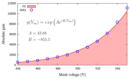
where is the number of electrons produced in each interaction, is the interaction rate, is the gain as a function of the anode potential . The gain as a function of the mesh potential is obtained experimentally by illuminating the Piggyback at low rates (see figure 10), expression that will be used afterwards with the corrected potential given by Va.
The charge is integrated considering the effect the accumulated charge will have in the gain at each time step. The simulation of each time step requires to know previously all the charges at each past time interval in order to apply the diffusion relation to them, this makes the computation of each time interval more expensive and the time required has a non-linear growth. The simulation of the first half an hour with reasonable accuracy can still be performed within a few hours. Figure 11 shows the charge evolution and the gain drop induced by a rate of 100 kHz/cm2, for a resistivity of 100 M and 1pF/mm2. As to compare with the experimental measurements we considered the number of electrons produced by an 8 keV event, Ne = 300 in an Ar+10%CO2 mixture.
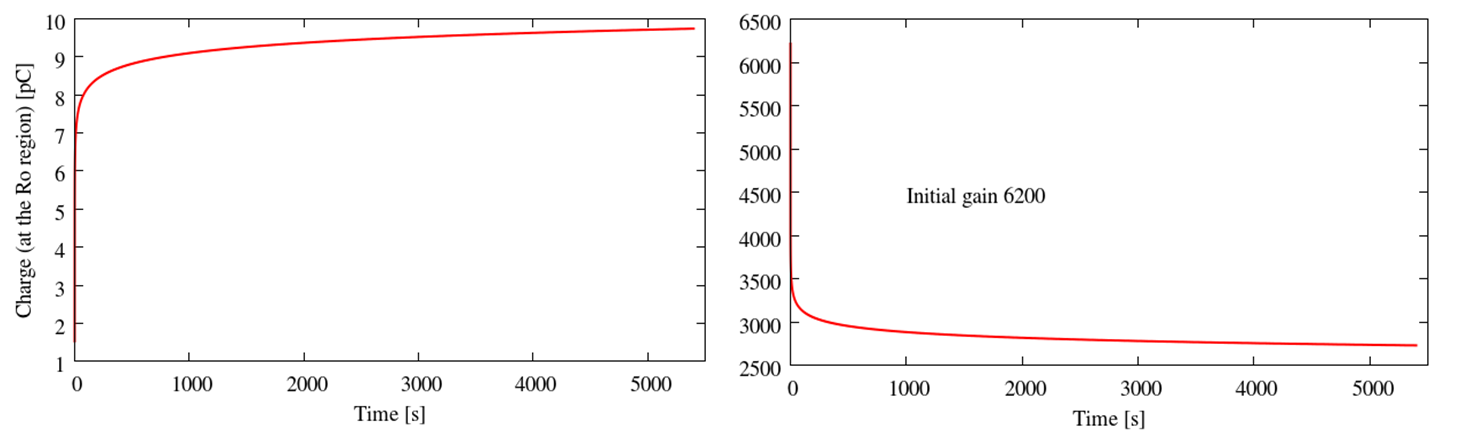
This simulation shows a fast gain drop of about 50% during the first seconds, and a second order drop of about 15% the next one hour and a half. This behavior is compatible with that observed on figure 3, considering that the first (fast) gain drop could not be observed in the measurement.
A set of simulations was launched at different scanning rates for different RC values in order to observe the effect on the gain drop observed. Figure 12 shows the final gain value obtained after an exposure of 5400 seconds, several simulations were performed at different rates in order to show the result as a function of the interaction flux. Different resistivity and capacitive values are tested from the range of 10M to 10 G, and from 0.5 pF/mm2 to 10 pF/mm2, showing the dependency with the applied rate for each case.
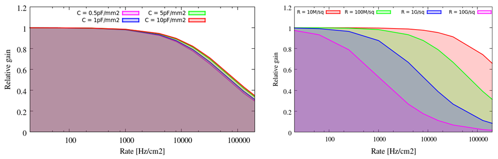
As lowest is the resistivity of the material, the longest is the flat gain region, and higher rates could be achieved without expecting an evolution in the gain, which of course, will also be faster for lower values of RC. The gain strongest dependency is with the resistivity of the foil, showing not strong dependency with the different capacitances simulated. However, the capacitance will have an important role in the charge diffusion time and thus in the stabilization time.
Finally, the measurements done with the X-ray generator allows to monitor the gain with the position of the 8 keV peak. In figure 13 the charge diffusion observed on the gain could explain the contribution to the observed effect on the gain drop.
The agreement between simulation and measurement could be biased by other effects such as grounding configuration, real resistivity value and homogeneity, and systematics induced in the experimental measurements which are constrained by the fact that the measurements should be made in a relative short period of time, but they also require a reasonable stabilization time.
6 CMOS chip read-out
Medipix2 [12] and Timepix [13] are CMOS chips which have been used as pixelated readout for Micro-Pattern Gaseous Detectors (MPGDs) [6, 14]. Both chips have the same size of 1416 mm2. They consist of a matrix of 256256 identical square pixels of 55 m side each. A regular topic associated to MPGDs is electronics protection to sparks. For this reason, layers of high resistivity material (amorphous silicon or silicon-rich nitride) have been deposited on CMOS pixel for discharge protection [15]. The Piggyback concept provides a spark protection by completely decoupling the detector from the electronics.
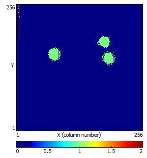
A 3020 mm2 bulk on a ceramic has been built to be used with Medipix2/Timepix chips. The amplification gap and the drift height were respectively 128 m and 10 mm. The ceramic was put on top a Medipix2 chip without gluing. The first image was recorded (see figure 10) using a 55Fe radioactive source. The mesh voltage was 430 V corresponding to a gain of about 105 in standard bulk in a gas mixture of argon and 5% isobutane. The detector was operating under such high gain for a whole day verifying the effectiveness of the spark protection scheme. The first results are extremely encouraging, demonstrating the proof of principle of this novel read-out architecture for the Micromegas detector.
7 Summary and outlook
We have fabricated and tested a new Micromegas detector with resistive anode deposited by an industrial process on a thin ceramic substrate. The first results are promising; the detector is stable, spark protected, provides a high gas gain and good energy resolution.
The new structure provides several advantages and opens new windows of opportunity in particle detectors. In particular:
-
(i)
The detector is completely dissociated from the read-out plane. This gives complete freedom to the user to choose the readout electronics card as a function of its needs; i.e. the card is easily adapted to the detector structure. As well it can be removed or replaced without switching off the detector
-
(ii)
In the case of integrated pixel chips this structure should solve the technical problem related to the implementation of many chips, without creating dead space, since no additional support of interface structure is needed.
-
(iii)
In the case of ceramic insulator there is an additional advantage: ceramics can provide large values of the dielectric constant which can reach values up to several thousand. This opens the possibility to select, when it is necessary, a thick insulator without violating the relation 1. With such large thicknesses the induced signal on the read-out strips could be spread-out to large values permitting the use of large size pads without degradation of the spatial resolution: the good spatial resolution is maintained by "pad charge sharing" [16, 17]. This is a big advantage compared to conventional Micromegas which needs narrow high-density anode readout element to achieve good spatial resolution.
-
(iv)
The proposed scheme provides a full spark protection. No additional protection structure is needed for the read-out electronic chip.
-
(v)
It is very easy to apply positive voltages on the micromesh and the anode and keep the cathode grounded, with no need of high voltage decoupling circuit for the anode signals. This can be important for the case that the cathode is also the entrance window.
-
(vi)
The detector materials, ruthenium oxide and ceramics, exhibit excellent outgassing properties. This is appropriate for high quality vacuum and it opens the way to seal the detector vessel.
Future developments are under way to improve smoothness and build larger surfaces. For small surfaces we would like to decrease as much as possible the thickness of the ceramic to improve the efficiency in the case of small pad readout chips like the TimePix.
For large-size detectors we could use thick ceramic substrate. This will produce large spread of the signals and could allow the usage of large read-out pads for applications where cost savings on electronics is required. Very large detector areas could be built using several ceramic structures mounted into a mosaic. To obtain a good flatness, tilts of the surfaces must be minimized and dead area can be reduced to a negligible level by precisely adjusting the ceramic substrates and by fixing them on top of the read-out strip or pixel plane. Interconnection of the various resistive films to the ground should be achieved through an appropriate technology that has to be developed. The Bulk process for fabricating the Micromegas gap could be applied over the global read-out area (mosaic).
References
- [1] H. Raether, Electron avalanches and breakdowns in gases. Washington: Butterworths, 1964.
- [2] I. Giomataris, Development and prospects of the new gaseous detector "Micromegas", \hrefhttp://dx.doi.org/10.1016/S0168-9002(98)00865-1 Nucl. Instr. and Meth. A, 419 (1998) p.239.
- [3] I. Giomataris, Ph. Rebourgeard, J.P. Robert, and G. Charpak, MICROMEGAS: A High granularity position sensitive gaseous detector for high particle flux environments, \hrefhttp://dx.doi.org/10.1016/0168-9002(96)00175-1 Nucl. Instr. and Meth. A, 376 (1996) p.29.
- [4] M. Dixit, et al., Micromegas TPC studies at high magnetic fields using the charge dispersion signal, \hrefhttp://dx.doi.org/10.1016/j.nima.2007.07.099 Nucl. Instr. and Meth. A, 581 (2007) p.254.
- [5] I. Giomataris, High Rate Applications of Micromegas and Prospects, \hrefhttp://arxiv.org/abs/physics/0610153 SNIC, vol. 0023, no. physics/0610153, 2006.
- [6] P. Colas, et al., The readout of a GEM or Micromegas-equipped TPC by means of the Medipix2 CMOS sensor as direct anode, \hrefhttp://dx.doi.org/10.1016/j.nima.2004.07.180 Nucl. Instr. and Meth. A, 535 (2004) p.506.
- [7] T. Alexopoulos, et al., Development of large size Micromegas detector for the upgrade of the ATLAS Muon system, \hrefhttp://dx.doi.org/10.1016/j.nima.2009.06.113 Nucl. Instr. and Meth. A, 617 (2010) p.161.
- [8] M.S. Dixit and A. Rankin, Simulating the charge dispersion phenomena in Micro Pattern Gas Detectors with a resistive anode, \hrefhttp://dx.doi.org/10.1016/j.nima.2006.06.050 Nucl. Instr. and Meth. A, 566-2 (2006) p.281.
- [9] J. Wotschak, Development of micromegas muon chambers for the ATLAS upgrade , \jinst72012C02021
- [10] I. Giomataris et al., Micromegas in a bulk, \hrefhttp://dx.doi.org/10.1016/j.nima.2005.12.222 Nucl. Instr. and Meth. A, 560 (2006), no. 2, p.405.
- [11] M. Kocsis et al., A novel gas-filled detector for synchrotron radiation applications, \hrefhttp://dx.doi.org/10.1016/j.nima.2006.01.117 Nucl. Instr. and Meth. A, 563 (2006) p.172.
- [12] X. Llopart, et al., Medipix2: A 64-k pixel readout chip with 55-m square elements working in single photon counting mode, \hrefhttp://ieeexplore.ieee.org/stamp/stamp.jsp?tp=&arnumber=1046904isnumber=22432 IEEE Trans. Nucl. Sci., 49 (2003).
- [13] X. Llopart, et al., Timepix, a 65k programmable pixel readout chip for arrival time, energy and/or photon counting measurements, \hrefhttp://dx.doi.org/10.1016/j.nima.2007.08.079 Nucl. Instr. and Meth. A, 581 (2007) p.485.
- [14] A. Bamberger, et al., Readout of GEM detectors using the Medipix2 CMOS pixel chip, \hrefhttp://dx.doi.org/10.1016/j.nima.2006.12.049 Nucl. Instr. and Meth. A, 573 (2007) p.361.
- [15] Y. Bilevych, et al., Spark protection layers for CMOS pixel anode chips in MPGDs , \hrefhttp://dx.doi.org/10.1016/j.nima.2010.11.116 Nucl. Instr. and Meth. A, 629 (2011) p.66.
- [16] F.J. Iguaz, et al., Micromegas detector developments for Dark Matter directional detection with MIMAC, \jinst62011P07002
- [17] J. Derré, et al., Spatial resolution in Micromegas detectors, \hrefhttp://dx.doi.org/10.1016/S0168-9002(00)01051-2 Nucl. Instr. and Meth. A, 459 (2001) p.523.