Quantum interference and Aharonov-Bohm oscillations in topological insulators
Abstract
Topological insulators have an insulating bulk but a metallic surface. In the simplest case, the surface electronic structure of a 3D topological insulator is described by a single 2D Dirac cone. A single 2D Dirac fermion cannot be realized in an isolated 2D system with time-reversal symmetry, but rather owes its existence to the topological properties of the 3D bulk wavefunctions. The transport properties of such a surface state are of considerable current interest; they have some similarities with graphene, which also realizes Dirac fermions, but have several unique features in their response to magnetic fields. In this review we give an overview of some of the main quantum transport properties of topological insulator surfaces. We focus on the efforts to use quantum interference phenomena, such as weak anti-localization and the Aharonov-Bohm effect, to verify in a transport experiment the Dirac nature of the surface state and its defining properties. In addition to explaining the basic ideas and predictions of the theory, we provide a survey of recent experimental work.
I Introduction
Topological insulators (TI) are bulk insulators with protected metallic surface states as a result of the topological properties of the bulk electronic wavefunctions.Hasan and Kane (2010); Moore (2010); Qi and Zhang (2011) For a three-dimensional topological insulator,Hasan and Moore (2011) this metallic state is a two-dimensional electron gas with many special features such as spin-momentum locking and a robustness to localization by disorder. While several of these features have been observed with surface sensitive probes such as angle-resolved photoemission spectroscopy, much of current experimental focus is aimed at demonstrating these and other surface state properties in transport measurements.
The main goal of this review article is to explain how the Aharonov-Bohm and other magnetotransport effects are manifested in topological insulator surface states and to summarize recent experimental and theoretical progress towards their observation. The Aharonov-Bohm effect can be utilized as a fundamental probe of how the quantum phase of an electronic wavefunction is sensitive to magnetic flux through the gauge invariance of the Schrödinger equation coupled to electromagnetic fields.Aharonov and Bohm (1959); Aronov and Sharvin (1987); Batelaan and Tonomura (2009) It is possible to give self-contained explanations of how the features of the surface state, which is modeled by a single massless Dirac cone in the simplest case, lead to unusual (as compared to in a traditional two-dimensional electron gas) magnetotransport behavior in a variety of experimentally relevant situations. This approach leaves out only the connection between bulk wavefunctions and surface electronic states, which requires a little bit of mathematical background and has been explained several times, for example in the reviews cited above.Hasan and Kane (2010); Moore (2010); Qi and Zhang (2011); Hasan and Moore (2011)
In the remainder of the introduction we discuss the basic properties of topological insulator surface states, concentrating on what makes them different from the two-dimensional electron gas (2DEG) in either conventional semiconductor heterojunctionsAndo (1982) or graphene.Castro Neto et al. (2009); Das Sarma et al. (2011) The main properties of the most common topological insulator materials are summarized and the relevant elements of quantum transport including the Aharonov-Bohm effectAharonov and Bohm (1959); Aronov and Sharvin (1987) and localization theoryBergmann (1984); Lee and Ramakrishnan (1985); Evers and Mirlin (2008) is given. While this review is mainly focused on the transport properties of 3D topological insulators, we comment at various points on the two-dimensional topological insulator or quantum spin Hall state,König et al. (2008) as observed first in (Hg,Cd)Te quantum wells.König et al. (2007) This phase is is interesting in itself and also illuminates some aspects of the three-dimensional behavior.
The main text consists of four sections. In section II we discuss the longitudinal conductivity which in the ideal case of insulating bulk should show ambipolar Hall effect and minimal conductivity when the chemical potential is tuned through the Dirac point. The main theoretical result covered is the absence of localization and the accompanying flow to the symplectic metal phase. Section III addresses magnetic field induced quantum oscillations such as the Shubnikov-de Haas (SdH) oscillations. We focus in particular on the signatures of the Berry phase of the Dirac fermion in the SdH signal. The quantum Hall effect is briefly discussed. Magnetic flux effects on quantum transport, such as weak anti-localization (WAL) and Aharonov-Bohm (AB) oscillations, are the subject of section IV. WAL is a useful probe of 2D transport but is insensitive to the Berry phase. In contrast, the AB oscillations can in principle be used to infer the presence of a nontrivial Berry phase. Finally, in section V we collect some related problems and future directions. We end the review with a summary and conclusion.
I.1 Surface states of three-dimensional topological insulators
In this section we introduce some key definitions and explain how the surface state of a topological insulator differs from a conventional two-dimensional electron system (cf. figure 1). Any strictly two-dimensional metal with time-reversal symmetry has a Fermi surface that consists of an even number of “sheets” (closed curves) once spin is included.Nielsen and Ninomiya (1981a, b) In the simple case of no spin-orbit coupling, the two sheets are degenerate; they move apart when spin-orbit coupling is included, but at every value of the Fermi energy the Fermi surface still consists of an even number of closed curves. The surface state of a topological insulator is not strictly two-dimensional in the sense that it consists of a boundary between two different three-dimensional bulk states, one of which is frequently the vacuum. It has an odd number of Fermi surface sheets, and in the simplest case that odd number is 1.
As an example, consider the model linear dispersion relation obtained with the Hamiltonian
| (1) |
where is the Fermi velocity, the momentum, and are the Pauli matrices. Another commonly used Hamiltonian differs only in the interpretation of the sigma matrices and their relation to the real spin. For experimentally relevant materials the details can be more complicated: the velocity is not simply scalar but depends on the direction,Fu (2009); Alpichshev et al. (2010); Kuroda et al. (2010) the spin polarization may be reduced from its maximal value,Yazyev et al. (2010); Pan et al. (2011); Souma et al. (2011); Okamoto et al. there may be more sheets of the Fermi surfaceHsieh et al. (2008) (i.e., an odd number larger than 1) and nonlinearity of the spectrum shows up away from the Dirac point.Shan et al. (2010); Culcer et al. (2010) Details of the surface geometry can also influence the electronic and spin structure.Silvestrov et al. (2012); Zhang et al. (2012, a) However, the Aharonov-Bohm effect and other magnetotransport phenomena discussed below are generally independent of these details. The “Dirac cone” energy-momentum relation described by (1) is shown in figure 1.
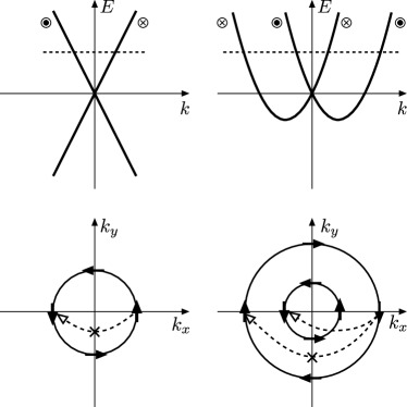
Time-reversal symmetry implies that the state at momentum must have spin direction opposite to that at . The spin direction therefore precesses as the electron momentum moves around the Fermi surface. This is often referred to as spin-momentum locking. This case is different from a “half-metal” where the spin polarization is constant and time-reversal symmetry is broken. As another comparison, adding the quadratic term to the above Hamiltonian gives a Hamiltonian commonly used to describe quantum wells with Rashba spin-orbit coupling.Winkler (2003) At every energy, there are either zero or two sheets of the Fermi surface (see figure 1).
In 3D, the bulk wavefunctions of a perfect crystal are characterized by four topological invariants that take values in , three “weak” and one “strong”.Moore and Balents (2007); Fu et al. (2007); Roy (2009) The latter is the one of greatest interest both experimentally and theoretically, and we will use the term “topological insulator” to refer to strong topological insulators where this invariant is nonzero. The existence of an odd number of Fermi surface sheets is a consequence of the odd value of the strong topological invariant. There are also some interesting features if the strong index is zero but one of the weak invariants is nonzero. Such “weak topological insulators” (WTI) have an even number of Dirac cones on the surface and can be viewed as layered versions of the two-dimensional topological insulator or quantum spin Hall state. The surface states of WTI’s are in principle less stable to either bulk or surface disorder since there exists perturbations that gap out the surface. It turns out, however, that when this perturbation is zero on average as in a random environment, the surface state is robust against localization. We discuss this in more detail in section V.1.
The low energy electronic structure of graphene is also described by two Dirac cones (ignoring the spin which does not play an important role in most graphene experiments). Graphene, however, has a time-reversal with and is therefore in a different symmetry class from TI’s which time-reversal symmetry satisfies . In the absence of intervalley coupling an effective time-reversal symmetry with emerges in graphene,Suzuura and Ando (2002) and the physics is that of a single Dirac cone. It is useful to keep this in mind since several results originally obtained for graphene are relevant to TI transport.
The two-dimensional topological insulator or quantum spin Hall state has the same locking of spin and momentum in its edge state as in the surface state described in (1): electrons moving one way along the edge have a certain spin orientation which is opposite that of the spin of the electrons moving in the reverse direction. There is a single branch of edge excitations moving in each direction, unlike in an ordinary quantum wire, which has two branches (spin-up and spin-down).
One simple difference in surface state transport between the 2D and 3D topological insulators can now be explained, and this will also help convey the importance of time-reversal symmetry. Time-reversal symmetry implies that every spin-half eigenstate is degenerate in energy with, and distinct from, its time-reversal conjugate (the state obtained by reversing the direction of time). As a result, every energy eigenvalue in a time-reversal invariant system of independent electrons is at least two-fold degenerate; these degenerate pairs are called Kramers pairs. Integer-spin particles can be equivalent to their time-reversal conjugates and there need not be such degeneracies. Now consider perturbing the original Hamiltonian. The robustness of Kramers pairs necessitates that any time-reversal invariant perturbation, such as potential scattering, has a zero matrix element between the two states of a pair, as otherwise it would split the pair.
As a consequence of the robustness of the Kramers pairs, elastic scattering at the edge of a 2D topological insulator disappears at low energy (in the gap), because the two available states belong to the same Kramers pair. The corresponding scattering from spin-up to spin-down is still forbidden in the case of an ordinary wire, but the scattering process that does not flip the spin is allowed and eventually leads to localization by disorder. In general, an even number of Kramers pairs of edge modes will localize, while an odd number will lose pairs until a single pair is left which cannot be localized. At low voltage and temperature, transport is effectively ballistic because backscattering disappears, although the corrections to the quantized conductance are expected to be power-law rather than exponential as in the quantum Hall case.Schmidt et al. (2012)
The same Kramers protection exists at the surface of a 3D topological insulator but is less powerful as now there are allowed scattering processes that do not violate the Kramers theorem. Scattering at any angle other than 180 degrees is allowed, and indeed Fourier transforms of STM measurementsRoushan et al. (2009) show the vanishing amplitude of perfect backscattering. Because there are still allowed scattering processes at leading order, unlike in the 2D case, the low-temperature fate of conduction at the surface of 3D topological insulator requires more thought and is discussed below in the context of weak localization theory.
I.2 Properties of topological insulator materials
In this review, we will focus on the basic physics of the topological insulator phase revealed through Aharonov-Bohm measurements and other magnetic effects on transport. However, in order to understand experiments, it seems useful to provide a few notes on the materials studied in current experiments, even though material improvements are rapid. In two dimensions the first demonstration of the theoretically predicted “helical” edge state was in (Hg,Cd)Te quantum wells.König et al. (2007) Recently, experiments were reported showing evidence for helical edge channels in InAs/GaSb quantum wells.Knez et al. (2011) There are theoretical proposals to realize the phase in other systems, e.g., when heavy atoms are adsorbed on graphene to increase the spin-orbit couplingWeeks et al. (2011); Hu et al. and in strained graphene in the presence of interactions.Abanin and Pesin (2012)
In the remainder of this section, we concentrate on the 3D state, where there are more materials and experiments. Bi-Sb alloys were the first materials studied for topological insulator behavior,Hsieh et al. (2008) but the high level of alloy disorder and the complicated surface Fermi surface (with 5 band crossings along the cut studied) have led to their being superseded by other materials, in particular the semiconductors Bi2Se3, Bi2Te3, Bi2Te2Se, and variations thereof.Zhang et al. (2009a); Valla et al.
Bi2Se3 is the 3D TI material that has been most investigated experimentally.Xia et al. (2009) It has a trigonal unit cell with five atoms, and can be pictured as having five layers Se-Bi-Se-Bi-Se; the central Se layer is clearly inequivalent to the outer two layers, and there is a good cleave plane between the van der Waals-bonded first and last Se layers. The bulk bandgap is approximately 0.3 eV. The surface Dirac velocity depends somewhat on the energy and the direction (there is a significant hexagonal distortion except very close to the Dirac point,Kuroda et al. (2010)) but an approximate value useful for theoretical estimates is m/s. These numbers are consistent with estimates from GW-improved DFT calculations.Yazyev et al. (2012) Estimates of the surface state spin polarization from photoemission and numerical calculations range from 60% of the spin half maximum up to nearly 100%.Yazyev et al. (2010); Pan et al. (2011)
Bi2Te3, also shown to be a topological insulator,Chen et al. (2009) has been studied for many years as a practical room-temperature thermoelectric material. It has the same structure as Bi2Se3 and a smaller bulk bandgap of 0.15 eV. Its thermoelectric utility can be understood from the rule of thumb that the ideal operating temperature of a thermoelectric semiconductor is about one-fifth of the bandgap . A significant power factor (product of electrical conductivity, temperature, and thermopower squared) depends on having an appreciable number of thermally excited carriers. Bi2Te2Se (“BTS”) has been studied very actively because crystals can be grown with bulk conductivity orders of magnitude lower than either Bi2Se3 or Bi2Te3.Jia et al. (2011); Xiong et al. (2012a) The Se atoms go in the middle layer of the five-layer structure. As opposed to Bi2Se3, which has the Dirac point in the bulk gap, the Dirac point in Bi2Te3 is buried deep in the valence band.
Considerable effort is going into finding 3D topological insulators and related phases in other materials families, whether to decrease the bulk conductivity or to find ordered phases that combine topological order with another type of order (e.g., antiferromagnetismMong et al. (2010) or superconductivity.Fu and Berg (2010)) The magnetotransport effects described below may be useful in identifying materials in the topological insulator phase when angle-resolved photoemission or other methods are impractical. In addition to the Bi based materials, straining 3D HgTe which is nominally a semimetal, opens up a gap and realizes a TI.Brüne et al. (2011) -Ag2Te has also been used in transport studies.Zhang et al. (2011a); Sulaev et al.
In early transport experiments the conductance was dominated by the bulk. The cleanest signatures of quantum interference from the surface state have been obtained in thin films and nanowires. These are either epitaxially grown or obtained with mechanical exfoliation. Due to the easy cleave plane, the thickness is generally a multiple of quintuple layers with each quintuple layer about 1 nm thick. In the ultrathin limit the tunnel coupling between the top and bottom surface is sufficiently large to open up a sizable gap and make the film insulating.Linder et al. (2009); Liu et al. (2010); Lu et al. (2010) This gap is observed experimentally in films a few nanometers thickZhang et al. (2009b); Liu et al. (2012a) and its rapid decay to zero with increasing thickness gives a direct measurement of the surface state’s penetration into the bulk that can be compared with photoemission results.Zhang et al. (2010) Insulating behavior in transport has also been observed.Cho et al. (2011, 2012); Taskin et al. (2012)
With increased surface mobility the possibility of realizing correlation physics opens up. One direction is fractional quantum Hall physics at the surface; indeed some features are observed in transport data that are conjectured as possibly indicating incipient fractional Hall states at the surface.Analytis et al. (2010a) A thin film of topological insulator in a magnetic field is analogous to a quantum Hall bilayer.Eisenstein and MacDonald (2004) These bilayers have been a fertile system for studies of many-body physics, as the proximity of the two layers enables interlayer correlated phases with remarkable properties when the Coulomb interaction between the layers is significant. However, these correlation effects may be hidden by the hybridization gap in topological insulator thin films.
I.3 Diffusive transport and the symplectic metal
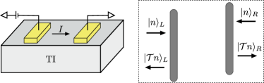
In the Altland-Zirnbauer symmetry classification,Altland and Zirnbauer (1997) the topological insulators we are interested in here belong to the symplectic class (AII in the Cartan notation). This symmetry class is characterized by the presence of a time-reversal symmetry. The time-reversal operator commutes with the Hamiltonian and satisfies . A two dimensional electron gas (2DEG) with strong spin-orbit coupling is also in the symplectic class, as well as graphene in the absence of intervalley scattering.Suzuura and Ando (2002) When the electronic transport is diffusive many of its characteristics are independent of the topological properties of the underlying system. We will refer to this state as the symplectic metal. The symplectic metal is characterized by weak anti-localization (WAL). Because of WAL the symplectic metal is, in the renormalization group sense, a stable fixed point. In this section we review the various characteristic quantum interference phenomena of the symplectic metal. We limit the discussion to two terminal transport. This ideal setup can for example model transport in one side of a large TI surface or conductance through a TI nanowire as schematically shown in figure 2.
The presence of a time-reversal symmetry crucially affects many of the transport properties of the symplectic metal. Before discussing the perhaps more intuitive path picture of the interference phenomena, we consider how these directly result from the symmetry constraints imposed by time-reversal symmetry on the scattering matrix describing the two terminal transport. In particular, we obtain absence of backscattering,Ando et al. (1998) discuss under what condition a perfectly transmitted mode is realized,Ando and Suzuura (2002) and give the connection between the time-reversal symmetry and weak anti-localization.
I.3.1 Quantum transport and time-reversal symmetry
The scattering matrix describing the two terminal transport in the presence of time-reversal symmetry with can be chosen to be antisymmetric. Before discussing the consequences of this antisymmetry we give a short derivation of this fact, following Ref. Bardarson, 2008.
Consider a two terminal setup as in figure 2. The left and right leads are metallic contacts which host a large number of incoming modes, denoted by and respectively. In a topological insulator these modes are the properly normalized eigenstates of the Dirac Hamiltonian (1). For example, if we assume periodic boundary conditions in the transverse direction, the modes can be written
| (2) | |||||
| (3) |
Here are the discrete transverse momenta with the transverse width of the sample, and the Fermi energy . We have assumed such that we can ignore the momentum dependence of the spinors. This is the relevant limit in the leads, which being metallic are highly doped.Tworzydło et al. (2006) These modes carry unit current . The outgoing modes are the time-reverse of the incoming modes and , since time-reversal reverses the direction of motion. Importantly, has the opposite spin to .
A solution to the Hamiltonian describing the system, subject to the boundary conditions imposed by the metallic leads at and , can be written
| (4) |
Since is a solution to the Schrödinger equation, the incoming coefficients and are linearly related to the outcoming coefficients and through the scattering matrix
| (5) |
Assuming an equal number of modes on the left and the right, the scattering matrix has the block diagonal form
| (6) |
where is the probability amplitude of reflection of mode into , and the other block matrices have a similar interpretation. For our current purpose we do not need to know the exact form of the wavefunction in the sample. In an actual calculation the scattering matrix is obtained from a knowledge of . The scattering matrix gives the two terminal conductance through the Landauer formula
| (7) |
where the second equation follows from current conservation . For ease of notation we also introduce the unitless conductance . The conductivity of a sample of width and length is given by .
Because of time-reversal symmetry, if is an eigenstate of the Hamiltonian so is . This solution, furthermore, is orthogonal to since
| (8) |
In the first equality we used the antiunitarity of , then that . is therefore an independent solution and all energy eigenvalues are doubly degenerate: the celebrated Kramers degeneracy. As a consequence
| (9) |
is also an allowed scattering state. By inspecting (4) we obtain
| (10) |
Comparing with Eq. (5) one concludes that time-reversal symmetry requires
| (11) |
with denoting the transpose. The antisymmetry of the scattering matrix gives rise to the absence of backscattering, the presence of a perfectly transmitted mode, and weak anti-localization, as we will now explain.
The absence of backscattering is simply the fact that the diagonal elements . This statement holds true both in a TI and a 2DEG, since it only requires the presence of a time-reversal symmetry. However, since is reflection of mode back into , which has the opposite spin, backscattering that does not flip the spin is allowed in the 2DEG (cf. figure 1). There is no such state in a TI and therefore backscattering is completely absent.
Due to the antisymmetry of , the eigenvalues of , and by unitarity also the transmission eigenvalues of , come in degenerate pairs. This is the Kramers degeneracy of transmission eigenvalues. Furthermore, if the number of modes is odd, there is necessarily at least one transmission eigenvalue that is equal to unity, since . This is the perfectly transmitted mode discussed by Ando and Suzuura,Ando and Suzuura (2002) and it will play a central role in our discussion below.
An odd number of modes can never strictly be realized in an inherently 2D system with time-reversal symmetry.Nielsen and Ninomiya (1981a, b) The absence of certain couplings can, however, reduce the system to an effective one with an odd number of modes. An example of this is graphene in the absence of intervalley coupling.Suzuura and Ando (2002) In contrast, a TI can intrinsically have an odd number of modes and therefore host a perfectly transmitted mode.
Weak anti-localization is the first order in quantum correction to the classical Drude conductance. To obtain WAL from the scattering matrix we assume the elements of to be randomly distributed Gaussian variablesBeenakker (1997) with
| (12) |
where the angular brackets denote average over the distribution of the elements of the scattering matrix. The delta function is needed to satisfy the antisymmetry condition (11) and the denominator is obtained from the unitarity of . Using this in the Landauer formula (7)
| (13) |
The first term is the classical conductance. It takes the value since each mode is equally likely to be transmitted as being reflected, due to the randomness of the scattering matrix. The second term is a positive enhancement of the conductance due to quantum interference, namely weak anti-localization. This term is absent in the absence of time-reversal symmetry, as is readily verified. A time-reversal breaking pertubation, such as a magnetic field, will therefore decrease the conductance. The fact that the first quantum correction is positive reflects the stability of the symplectic metal phase to weak disorder. This correction is perturbative (here in ) and independent of topology and is therefore the same for TI surfaces and a 2DEG. The case of strong disorder and small conductance is discussed in section II.2.
This argument is instructive in that it shows the relation between WAL and time-reversal symmetry. The assumption (12) is however only strictly valid when the two leads are connected by a quantum dot.Beenakker (1997) We are interested in the case of a two dimensional sample connecting the two leads. This will be discussed in the next section.
I.3.2 Weak anti-localization and Berry phase
When a Dirac fermion traverses a loop in space, the spin rotates by due to the spin-momentum locking. The wave function, being a spinor, acquires a phase of which can alternatively be considered as a Berry phase induced by the Dirac point. This phase affects quantum interference and in particular changes the constructive interference of spinless fermions that gives rise to weak localization into destructive interference and WAL.
Studies of weak (anti)-localization date back a couple of decades and the physics is by now well understood. A number of reviewsBergmann (1984); Lee and Ramakrishnan (1985) and textbooks (our discussion is of similar flavor asAkkermans and Montambaux (2007)) exist that discuss the basic phenomena. The importance of spin-orbit coupling and the resulting WAL correction was first derived by Hikami, Larkin and Nagaoka.Hikami et al. (1980) An intuitive picture has been given by Bergmann.Bergmann (1983) The details of the derivation for Dirac fermions are slightly different, but the final answer for the WAL correction is the same, as shown by Suzuura and AndoSuzuura and Ando (2002) and McCann et al.McCann et al. (2006) in the context of graphene. This is to be expected since the two systems are in the same universality class. Nevertheless, we include here a short introduction to the topic, focusing on the broad physical picture and avoiding detailed formalism. This should serve as a guide to the literature and to make this review more self-contained. In particular, we will need some of the results discussed in this section in our later survey of TI transport experiments. In the context of TI’s the WAL correction has been discussed further theoretically by several authors.Imura et al. (2009); Tkachov and Hankiewicz (2011); Lu et al. (2011); Lu and Shen (2011); Garate and Glazman (2012); Adroguer et al. ; Krueckl and Richter
As in the last section we focus on the two terminal setup and the conductance in terms of the scattering matrix. Reflection and transmission amplitudes can be written as a sum over all possible paths connecting the two leads (see figure 3).
| (14) | |||||
| (15) |
Here denotes paths that enter the sample from mode in the left lead and exit through mode in the same lead. Similarly, denotes paths that start in mode in the left lead and exit through mode on the right. is the classical action of path and contains the stability amplitude, normalization and possible geometric phases of the path .Gutzwiller (1990); Haake (2010) In particular, any phase acquired from rotation of the spin degree of freedom will enter through . Generally, the effect of the spin rotation is captured by a matrix valued amplitudeZaitsev et al. (2005) but this is not needed for our current purpose due to the spin-momentum locking.

In terms of reflection amplitudes, the conductance (7) is given by
| (16) |
When averaging over disorder, the quickly oscillating exponential term will generally average to zero, unless . The classical Drude conductance is obtained by including only the diagonal terms . In addition, interference terms where with the time-reverse of survive the disorder average since by time-reversal symmetry . The amplitudes and have the same absolute value, but have a phase difference of , and thus . This is due to the Berry phase picked up by the relative rotation of the spin between the two paths, see figure 4. Therefore the total contribution of these two paths to the sum in (16) is
| (17) |
This is the absence of backscattering obtained from symmetry in the last section. Compared to the classical value , the probability to reflect back into the same lead is reduced and the conductance is enhanced. Note that this destructive interference only affects the diagonal elements of the matrix of reflection amplitudes.

This is not the full story, as one infers from the fact that such paths do not affect the conductance when written in terms of transmission amplitudes
| (18) |
Indeed, if goes from the left lead to the right lead, the time-reversed path goes from the right lead to the left lead and therefore does not enter the sum (18). With no change to the transmission amplitudes as compared with the classical value, current is no longer conserved and the scattering matrix is not unitary if we include only these paths. To get a consistent, current conserving theory, we need to include additional paths. These are the paths that have a single self crossing (figure 3), and the corresponding path which is almost the same except for an avoided crossing at the crossing point.Aleiner and Larkin (1996) The two paths therefore traverse the loop in the path in opposite direction. The sign of the correction to the amplitude is determined by the phase picked up in the loop and the details of the encounter at the crossing.Richter and Sieber (2002) Instead of going through the derivation, we can simply infer the sign of the correction from the absence of backscattering and the need to obtain a unitary scattering matrix. In addition to the paths that end up in the opposite lead after leaving the loop, there are paths that instead return to the same lead and therefore affect reflection probabilities. The interference of the loop is independent of which lead the particle ends up in after leaving the loop. Thus, the correction from these loops has the same sign for reflection and transmission probabilities. This correction is therefore necessarily positive to compensate the negative contribution due to the absence of backscattering. Transmission is enhanced by the quantum interference giving rise to WAL. In this sense absence of backscattering and WAL are integrally related through current conservation.
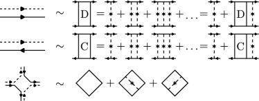
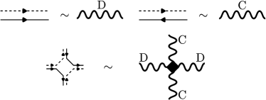
In the next step we focus on the quantum corrections to the conductance as interference between the paths and as depicted in the diagram of figure 3b. Instead of having the diagram denote only two paths we reinterpret it as a sum of many paths. Decomposing the diagram into parts, each part has an interpretation which corresponds to an object that is commonly obtained in diagrammatic calculations of the conductivity. This connection between the path picture of WAL and the diagrammatic calculation aids the intuitive understanding of the latter.
To that end, we decompose the diagram of figure 3b into three main parts. The first part represents the sum of all possible pair of paths that travel together from the lead towards the crossing point. This includes paths that are scattered by a single impurity, two impurities, and so on. Since they travel together, the two paths scatter of the same set of impurities in the same order. This is equivalent to the “diffusion” in the diagrammatic language and naturally satisfies a diffusion equation. Essentially, a density disturbance is injected at the lead and diffuses towards the crossing point. The second part is the loop, which the two paths traverse in opposite direction. The paths again scatter of the same set of impurities, but now in the opposite order. In the diagrammatic language this corresponds to the “cooperon”. When time-reversal symmetry is preserved, it also satisfies a diffusion equation. The last part is the crossing point, where the paths switch from traveling together to traveling in the opposite direction. This corresponds to the Hikami box in the diagrammatic language.
To find the correction to the conductivity we need to estimate the number of paths with a single self-crossing. This is equivalent to calculating the probability for the cooperon to return back to the crossing point. Since it satisfies a diffusion equation, in time this probability is proportional to . It does not matter at what time the crossing happens, as long as the time is smaller than the phase coherence time after which the paths are no longer phase coherent. Integration over time gives
| (19) |
The lower bound is given by the mean free time , below which the motion is ballistic, and the dephasing length with the diffusion constant. In the last equality we have assumed the temperature dependence of the dephasing to be given by a power law with . is defined by the relation . We have not explicitly kept track of the prefactors, since our main goal here is to give a phenomenological understanding of the origin of the logarithmic dependence of the WAL correction. Details can be found for example in Ref. Akkermans and Montambaux, 2007.
We have described a current conserving theory of WAL that takes into account paths with a single self crossing. In principle, there are additional paths with a larger number of crossings and these also give arise to interference correction. One can show that including only the single crossing paths is equivalent to assuming , with the Fermi momentum and the mean free path.Akkermans and Montambaux (2007) This is the same condition required for the validity of most diagrammatic calculations. More crossings give higher order corrections in , and are eventually responsible for localization (see e.g. Ref. Müller et al., 2007 and references therein for a description of such higher order paths in chaotic transport).
In theoretical work on quantum transport of Dirac fermions, the WAL correction (19) is often used to identify the symplectic metal. For example, in section II.2 on the absence of localization and section V.1 on transport in WTI’s, a logarithmic dependence of the conductance on the system size (replacing the phase coherent length in finite systems) with a slope is observed. Experimentally, is is often easier to observe WAL by applying a magnetic field. The magnetic field breaks time-reversal symmetry and changes the interference of the cooperon such that eventually the WAL correction disappears. This is the subject of the next section.
I.3.3 Aharonov-Bohm and Altshuler-Aronov-Spivak magnetoconductance oscillations
In the presence of a magnetic field perpendicular to the 2D motion, the paths pick up the Aharonov-Bohm (AB) phaseAharonov and Bohm (1959); Aronov and Sharvin (1987)
| (20) |
with a vector potential of the magnetic field , and the integration is along the path . If the path is a closed loop, the integral is equal to the flux through the loop and the Aharonov-Bohm phase becomes , with the magnetic flux quantum. The AB phase can both lead to periodic oscillation of the conductance and destruction of WAL.
We assume the magnetic field is weak enough not to affect the classical motion on the time scale of the mean free time , i.e. that with the cyclotron frequency. The diffusion constant, and consequently the Drude conductivity, therefore remains unchanged. In the diffusion the two paths pick up the same phase which is then canceled. In the loop (cooperon) the two paths pick up the opposite phase. This modifies the diffusion of the cooperon which now satisfies a diffusion equation with . Solving the modified diffusion equation, one finds that the return probability is proportional to .Akkermans and Montambaux (2007) The WAL correction takes the form
| (21) |
where and is the digamma function. The characteristic magnetic field strength needed to destroy the phase coherence of the cooperon, and thereby the WAL, corresponds to a flux quantum through the loop. Since the first digamma function is often replaced by its asymptotic form, resulting in the Hikami-Larkin-Nagaoka expressionHikami et al. (1980)
| (22) |
We have introduced the factor which is simply equal to here, but will be useful in comparing with experiments below.
A magnetic field can also give rise to periodic oscillations in the conductance when the surface is multiply connected. This is realized for example in TI nanowires, where if the bulk is insulating the surface acts as a hollow metallic cylinder. Applying flux along the wire introduces a phase to each path that loops around the cylinder times. This modifies the WAL correction in a sample of width and length to be
| (23) |
up to an unimportant constant. The magnetoconductance oscillates with a period of . The factor of two originates in the interference between clockwise and anti-clockwise circulating paths that each pick up a flux . This type of oscillations where originally discussed by Altshuler, Aronov and Spivak in the context of metallic cylinders,Altshuler et al. (1981) and experimentally observed by Sharvin and Sharvin.Sharvin and Sharvin (1981) For this reason they are often referred to as AAS oscillations in the literature (for a review see Ref. Aronov and Sharvin, 1987). Away from the symplectic metal limit the magnetoconductance of the TI nanowire can realize robust oscillations with period , double that of the AAS oscillations. This is discussed in section IV.2.
I.3.4 Universal conductance fluctuations
Weak anti-localization is a quantum correction to the average conductance. For a given sample, as external parameters are varied, the conductance fluctuates around the average due to quantum interference. The amplitude of the fluctuations is universal (independent of microscopic parameters) and of the order of . These are the universal conductance fluctuations (UCF). Like WAL, the UCF amplitude is determined by the symmetry class and is a characteristic of the symplectic metal that is independent of topology. The UCF can be understood in terms of the path picture of the last section. We will not discuss this here and instead refer for example to Ref. Akkermans and Montambaux, 2007 for details and further references.
In the context of Dirac fermions the UCF was studied theoretically in Refs. Cheianov et al., 2007; Rycerz et al., 2007; Kechedzhi et al., 2008; Kharitonov and Efetov, 2008; Rossi et al., 2012. UCF has been observed experimentally in TI’s in several experiments and its temperature dependence used to estimate the phase coherence length Checkelsky et al., 2011; Matsuo et al., 2012; Li et al., . Anomalously large conductance fluctuations were observed in large Bi2Se3 crystals,Checkelsky et al. (2009) presumably because of the large bulk conductivity.
I.3.5 Field theory of diffusion
In our discussion of WAL we have employed a semiclassical path picture and provided its connection to diagrammatic calculations. Another theoretical approach that is commonly adapted in localization studies is the field theory approach. The field theory describing diffusion is the non-linear sigma model (NLM).Efetov (1997) The fields in the NLM live on a manifold that is determined by the symmetry class. In some cases, these manifolds allow the presence of a topological term, that is a term that only depends on the topology of the field configurations, in the NLM. The localization properties depend strongly on the presence or absence of the topological terms (cf. section II.2).
To have a picture in mind, we provide a connection between the NLM and the semiclassical path approach. The propagators of the fields in the NLM are given by the diffusion and the cooperon, see figure 6. The non-linearity of the NLM corresponds to interactions between the cooperons and diffusions. In particular, the four field interaction vertex corresponds exactly to the Hikami box, or the crossing point. Higher order interaction vertices correspond to interference between paths with more than one self-crossing.Hikami (1981)
The coupling constant in the NLM is related to the conductivity of the system. The WAL correction, as depicted in figure 3, is the one-loop renormalization of this coupling constant. Higher order correction have been calculated and in the symplectic metal the next nonzero correction is only obtained at four-loop order (the calculation has been carried out to five-loops).Hikami (1992) This is one reason why the WAL correction (19) describes numerical simulations very well already at not too large conductivity and system size (cf. section II.2).
II Longitudinal conductivity of topological insulator surfaces
In graphene, the key observations confirming the Dirac nature of the charge carriers were the anomalous quantum Hall effect and the ambipolar field effect with the accompanying minimum conductivity.Castro Neto et al. (2009); Das Sarma et al. (2011) Observation of these effects in TI’s would constitute a convincing step towards verifying through transport experiments the Dirac dispersion of the surface states. Magnetic field and flux effects on quantum transport, including the quantum Hall effect, will be discussed in detail in the next two sections. In this section we focus on the zero field longitudinal conductivity and the absence of localization.
II.1 Ambipolar field effect
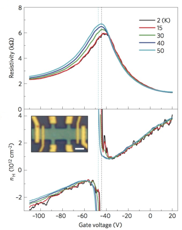
Observation of minimum conductivity and ambipolar field effect requires the conductance to be dominated by the surface. Progress towards that end has been made by reducing the bulk density by doping and using thin films. Several groups have reported minimum conductivity and/or ambipolar field effect.Steinberg et al. (2010); Ren et al. (2011); Kong et al. (2011); Sacépé et al. (2011); Hao et al. (2012); Kim et al. (2012) As an example, figure 7 shows experimental data demonstrating both a minimum conductivity and an ambipolar Hall field effect in Bi2Se3 thin films. As in graphene the minimum conductivity depends only weakly on temperature. The Hall density is linear in the gate voltage at low and high gate voltage, suggesting that the charge carriers are of only one type. Together these results indicate that the transport is through a surface state rather than being obtained from the bulk.
In graphene the minimal conductivity is understood in terms of the physics of electron and hole puddles induced by disorder (for a review see Ref. Das Sarma et al., 2011). The same is likely to hold true in TI transport, with nonlinearities in the spectrum away from the Dirac point playing a more important role than in graphene.Culcer et al. (2010); Adam et al. (2012) In fact, electron hole puddles have already been observed in STM experiments.Beidenkopf et al. (2011) This is an important and current area of theoretical and experimental interest. It is, however, outside of the scope of this review which focuses more on the quantum correction to the conductivity. We will therefore not discuss it further, but rather briefly review the quantum theory of the longitudinal transport, single parameter scaling and the absence of localization. The results of these considerations will be of relevance to later discussion of WAL and quantum transport in WTI’s, and is of fundamental interest by itself.
II.2 Absence of localization
The surface of a strong TI is topologically protected from Anderson localization.Fu and Kane (2007); Ryu et al. (2007); Ostrovsky et al. (2007); Bardarson et al. (2007) Instead, disorder always drives the surface into the stable symplectic metal phase.Bardarson et al. (2007); Ryu et al. (2007) This even holds at the Dirac point, where in the clean case the density of states goes to zero and the condition for the perturbative calculation giving WAL () does not hold. The surface transport in TI’s is therefore always diffusive at low enough temperature and characterized by WAL.
Anderson localizationEvers and Mirlin (2008) generally happens in 2D electronic systems when the dimensionless conductance . In this regime, the perturbative calculations of section I.3 are not valid and one needs to rely on numerical simulations. In figure 8 we show numerical results demonstrating the flow of the conductivity with increasing system size towards that of the symplectic metal.Bardarson et al. (2007); Nomura et al. (2007) At large enough the conductivity increases logarithmically with a slope consistent with WAL (19). The scaling function is strictly positive,Bardarson et al. (2007); Nomura et al. (2007) as opposed to the normal 2D electron gas with spin-orbit coupling which has a metal-insulator transitionMarkoš and Schweitzer (2006); Evers and Mirlin (2008) (and therefore a sign change in ) at .
The topological nature of the protection from localization can be understood by exploring the dependence of the energy spectrum on the boundary condition.Fu and Kane (2007); Nomura et al. (2007) Specifically, figure 9 shows the sensitivity of the energy levels of a disordered Dirac fermion in a finite sample to a twist in the boundary condition . At and the system is time-reversal symmetric and the spectrum is Kramers degenerate. Going between these two special values the Kramers pairs exchange partners.Nomura et al. (2007) This pair switch is a topological property and disorder can not change this behavior. The band width is always of the order of the mean level spacing and by Thouless argumentLee and Ramakrishnan (1985) the conductance is at least and localization can not take place. Indeed, a localized state is unaffected by changes in the boundary conditions and its energy is independent of the boundary flux and . In a conventional 2DEG the Kramers partners do not switch pairs and localization ensues for strong enough disorder. The switch versus no switch of Kramer’s partners reflects the nature of the topological classification of 3D time-reversal invariant TI’s.Fu and Kane (2007)
At the field theory level, the difference between a single Dirac fermion and a 2DEG is understood to be due to the presence or absence of a topological term in the NLM respectively.Ryu et al. (2007); Ostrovsky et al. (2007) The 3D TI is thus characterized by a topological term in the effective field theory of diffusion at the surface which is in one lower dimension. Generalizing this notion to all dimensions and symmetry classes one can classify all possible topological insulators and superconductors by the possibility of realizing a topological term in the corresponding NLM.Schnyder et al. (2008)
III Magnetotransport in crystals of 3D topological insulator materials
III.1 Shubnikov-de Haas oscillations and quantum Hall effect
As a prelude to discussing the Aharonov-Bohm effect and other flux effects in the following section, we now discuss standard magnetoconductance measurements on 3D topological insulators. Electrical transport in a 3D topological insulator receives contributions from both bulk and surface states. A goal of much current research is to find 3D topological insulator materials that are truly insulating in the bulk, as defined for example by a resistivity that shows activated behavior at low temperature (i.e., diverges exponentially as , where is the bandgap, up to power-law factors). This has been difficult to achieve, and in the few cases where a divergence of this form is seen, the effective bandgap is much smaller than the expected bandgap from either photoemission calculations or electric structure theory.Skinner et al.
Magnetotransport measurements provide a natural means to distinguish between bulk and surface transport when the bulk retains a nonzero conductivity. Ideally, a sample can be made sufficiently clean that both bulk and surface contributions will show magnetoconductance oscillations, the Shubnikov-de Haas (SdH) oscillations. Such oscillations are periodic in inverse magnetic field with period
| (24) |
where is the cross-sectional Fermi surface area transverse to the applied field. This is an area in -space, which has dimensions of inverse area, so the oscillation period is essentially an area divided by the flux quantum, up to a numerical factor. An ideal 3D topological insulator with one bulk Fermi surface and one surface Fermi surface will show two periods in the magnetoconductance oscillations, and these two oscillations will be distinguished by different areas and different angular dependences, assuming that the bulk Fermi surface is less two-dimensional than the surface one.
In a strictly two-dimensional electron system, SdH oscillations occur as a precursor of the quantum Hall effect. On a quantum Hall plateau the diagonal resistivity drops to zero (note that the tensorial nature of implies that the diagonal components of both resistivity and conductivity are zero). The locations of the Landau levels in a conventional 2DEG are at half-integer multiples of the cyclotron energy , , with At fixed Fermi level in the 2DEG, as is achieved if the 2DEG is in contact with a reservior, the condition for the th Landau level to cross is , or
| (25) |
So these features are equally spaced in , but with an offset of . In an STI this offset is absent because the spectrum is Dirac-like: including a Zeeman term for later reference, the Landau levels for a Dirac cone of velocity occur at
| (26) |
where the first term is the Zeeman effect and the second gives an dependence. For zero Zeeman effect, the Landau level crossings occur at
| (27) |
so now with no offset, as promised. Hence a “Landau level index plot” (“fan diagram”) can in principle distinguish between the case of a quadratic spectrum and a Dirac spectrum.
In the SdH regime the same difference in offset shows up in the phase of the quantum oscillation. However, in SdH oscillations the diagonal resistivity and conductivity oscillate out of phase, while in the quantum Hall regime they move in-phase. For example, in the quantum Hall regime both are zero on a plateau as the resistivity and conductivity are purely off-diagonal tensors. A useful reference for SdH oscillations is the book of Shoenberg;Shoenberg (1984) here we focus on the key differences between Dirac and ordinary (quadratic) fermions. A basic assumption in the following conventional theory is that the only effect of the magnetic field is that its coupling to the orbital degrees of freedom is essentially as a “probe”: it does not modify the electronic structure except through this orbital effect. As high magnetic fields have to be used to observe oscillations, in part because the surface electron density is high and mobility is not much higher than V/(cm2/s) in current samples even at low temperature, this assumption needs to be considered carefully, especially in possible future materials where the surface topological state results from correlation phenomena that are sensitive to magnetic field.
The two cases of SdH oscillations (normal 2DEG and Dirac fermions) can be obtained starting from the semiclassical quantization of energy levels:
| (28) |
where is the Landau level index of the oscillation, is the cross-sectional Fermi surface area at energy and the shift for a conventional 2DEG and for an STI. As emphasized by Mikitik and Sharlai,Mikitik and Sharlai (1999, 2012) the shift is quantized to one value or the other depending only on the number of Dirac points; details of energetics are unimportant. While this semiclassical formula is only generally valid for large , note that for in a conventional 2DEG, we obtain for Landau level
| (29) |
consistent with the quantum Hall limit. For the Dirac case, we obtain at Landau level
| (30) |
again consistent with the exact calculation.
In practice the strength of the oscillations is reduced by both disorder and thermal fluctuations. The Lifshitz-Kosevich formula can be applied to estimate the strength of the oscillations incorporating this shift; in the simplest case (for additional corrections, see Ref. Ando, 1974; for experimental examples, see Ref. Fang et al., and references therein),
| (31) |
is the oscillatory component of the resistance . Here is the Dingle damping factor from disorder,
| (32) |
where is the scattering time, and describes reduction due to thermal smearing. One recent theoretical analysisMikitik and Sharlai (2012) of SdH experiments in Bi2Se3 and Bi2Te3 specifically for this phase argues that all experiments are consistent with once effects of nonzero chemical potential and Zeeman energy are taken into account. Our discussion here has been in terms of flat infinite surfaces. The QHE effect on finite curved and multiple connected surfaces has been explored theoretically in Refs. Lee, 2009; Vafek, 2011; Sitte et al., 2012.
There are several factors, some fundamental and some material-dependent, that complicate the observation of this physics in a 3D topological insulator. First, while the bulk of a topological insulator probably does serve to some extent as a reservoir of electrons for the surface state at a fixed chemical potential, this ignores surface charging effects and also ignores the dependence of bulk electron properties on applied magnetic field. Second, in transport the overall measured conductivity or resistivity always include a significant bulk contribution in current materials, although impressive progress has been made in reducing the bulk contribution.
Another complication is that the factor may be significantly larger than 2 (as large as 30-50); this is known to be the case for bulk electrons in Bi2Te3, Bi2Se3, and HgTe materials as a consequence of the same relativistic effects that lead to the TI behavior. Electronic structure calculation of the factor of the surface state is technically challenging, but STM experiments and most transport experiments are consistent with so that the Zeeman effect is relatively weak compared to the orbital effects. A “smoking gun” for the Zeeman effect is that the zeroth Landau level’s energy is solely determined by the Zeeman effect, so observation of the zeroth level at high fields would allow a fairly direct measurement of the Zeeman effect, but this requires starting with a sample whose chemical potential is close to the Dirac point. Some intrinsic interest of the Zeeman effect in the surface state is that it does not commute with the starting Hamiltonian, unlike in either graphene or a conventional 2DEG (assuming spin-orbit coupling can be neglected). As a result, the Zeeman effect modifies the eigenstates, not just their energies, and opens up an energy gap even if the orbital field is excluded.
III.2 Experimental observations of Shubnikov-de Haas oscillations and the quantum Hall effect
Early observations of quantum oscillations were dominated by the bulk.Analytis et al. (2010b); Eto et al. (2010); Butch et al. (2010) From the SdH oscillations the anisotropic nature of the bulk Fermi surface is verified. This anisotropy also shows up in angular-dependent magnetoresistance oscillations.Eto et al. (2010); Taskin et al. (2010) For these samples with large bulk conductance, a good characterization of these bulk contributions is required to extract any possible surface contribution. This may require very large fields.Analytis et al. (2010a)
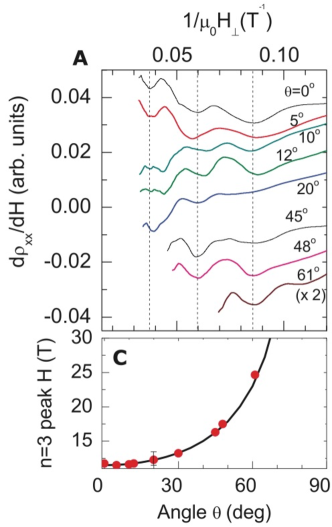
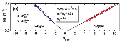
Alternatively, in samples with larger surface contribution, clear 2D SdH oscillations are observed.Qu et al. (2010); Analytis et al. (2010a); Ren et al. (2010); Taskin et al. (2011); Ren et al. (2011); Wang et al. (2012); He et al. (2012); Xiong et al. (2012a, b); Petrushevsky et al. (2012) The 2D nature of the SdH oscillations is for example revealed by tilting the magnetic field. The 2D SdH only depends on the perpendicular component of the magnetic field, and therefore the position of resistance maxima varies as . An example of SdH oscillations in Bi2Te3 is shown in figure 10. The position of the maxima in the resistance can in principle be used to extract the value of the Berry phase through the shift introduced in the last section. Most experiments have been interpreted to be consistent with a non-trivial Berry phase, though an accurate extraction of its value is complicated by nonlinearites of the spectrum and a nonzero factor.Taskin and Ando (2011); Xiong et al. (2012a); Petrushevsky et al. (2012) An example of a Landau level fan diagram is given in figure 11. In many samples the doping level of the surface is time dependent due to aging effects. By using this time dependence it was possible to probe both electron and hole transport in the same sample.Taskin et al. (2011)
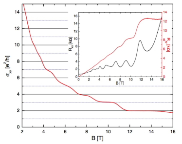
While there are several works that report SdH oscillations, a fully developed QHE is rare though signatures of the QHE have been reported.Cheng et al. (2010); Hanaguri et al. (2010); Brüne et al. (2011) In particular, figure 12 shows the Hall conductance obtained in strained HgTe with plateaus at multiples of . The appearance of plateaus at even values of is interpreted to be a consequence of a different filling factor in the top and bottom surfaces. The longitudinal conductance does not go to zero at the plateaus, presumably due to the side surfaces remaining conductive.
A quantized Hall effect and SdH oscillations with dependence have also been observed in highly doped samples, known to be dominated by the bulk,Cao et al. (2012) and interpreted as evidence of layered bulk transport. As opposed to the surface data, these layered SdH oscillations where consistent with zero Berry phase. Finally we mention that related quantum oscillations have also been observed in other quantities, such as magnetization.Taskin and Ando (2009); Kim et al. (2011a); Lawson et al.
IV Magnetic flux effects on quantum transport in topological insulator surfaces
In this section we discuss two related effects of magnetic flux on quantum transport, weak anti-localization and Aharonov-Bohm or Altshuler-Aronov-Spivak oscillations. While these are often viewed as separate effects, they all arise from the AB phase of the wave function and quantum interference between paths. In particular, WAL and AAS oscillations are exactly the same phenomena except they are realized in samples with different topology (flat versus multiply connected). When coupled with the Berry phase, AB oscillations of seemingly different nature can arise as discussed below. The distinction between the AB and the AAS oscillations is really that the former is realized when the particle motion is ballistic or pseudo-diffusive, while the latter are obtained in the diffusive state. An important difference between the two cases is that in the diffusive state, as we discussed in the introduction, one can not distinguish between a TI and a normal 2DEG. This is in principle possible with the AB oscillations.
IV.1 Weak anti-localization in thin films
Since the surface state is always driven into the symplectic metal phase, one expects to observe weak anti-localization. WAL can both be observed as a negative magnetoconductance (22) and as a logarithmic temperature enhancement of the conductivity (19). We will discuss the two approaches separately in the following. To avoid having the WAL signal being completely masked by bulk effects most experiments to date work with thin films. These are mostly Bi2Se3 filmsHirahara et al. (2010); Chen et al. (2010); Liu et al. (2011); Checkelsky et al. (2011); Chen et al. (2011); Wang et al. (2011); Kim et al. (2011b); Steinberg et al. (2011); Liu et al. (2012b); Matsuo et al. (2012); Takagaki et al. (2012); Zhang et al. (b); Bansal et al. but studies with Bi2Te3He et al. (2011) and Bi2(SexTe1-x)3Cha et al. (2012) have also been reported. To further reduce the bulk conductivity the films are sometimes additionally doped, for example with Ca,Checkelsky et al. (2011) PdWang et al. (2011) or Cu,Takagaki et al. (2012) or the Fermi level is moved into the bulk gap with the help of a gate voltage on a back gateChen et al. (2010); Checkelsky et al. (2011); Chen et al. (2011) or a top gate.Steinberg et al. (2011) The effect of magnetic doping and the resulting crossover to weak localization (WL) has also been studied, both experimentallyLiu et al. (2012b) and theoretically.Lu et al. (2011)
IV.1.1 Magnetic field dependence of weak anti-localization
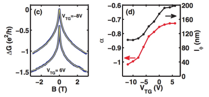
Most experiments observe a negative magnetoconductance consistent with (22) but with a prefactor that varies roughly in the range .Hirahara et al. (2010); Chen et al. (2010); Liu et al. (2011); Checkelsky et al. (2011); Chen et al. (2011); Wang et al. (2011); Kim et al. (2011b); Steinberg et al. (2011); Liu et al. (2012b); Matsuo et al. (2012); Takagaki et al. (2012); Zhang et al. (b); He et al. (2011); Cha et al. (2012) The value of can be tuned by as much as a factor of two in a single sample by varying gate voltageChen et al. (2010, 2011); Steinberg et al. (2011) (see figure 13). Both the broad range of values obtained for and its gate voltage tunability can be understood by carefully taking into account the bulk contribution and the coupling between surface and bulk. Some of this physics was discussed theoretically in Ref. Lu and Shen, 2011 and later in detail in Ref. Garate and Glazman, 2012. We give a simplified discussion of the results of Ref. Garate and Glazman, 2012 here and refer to the original works for further details.
When the thickness of the film , the bulk is effectively two dimensional and contributes 2D quantum correction of its own. Generally, due to the strong spin-orbit coupling in TI materials, this is also a WAL of the form (22) with . However, if the bulk is only weakly doped and intervalley and spin scattering in the bulk is negligible, a WL with is obtained instead. Roughly speaking, this is because the spin of the eigenstates close to the band edge depends only weakly on the momentum. The Berry phase from the spin rotation is thus absent. It is likely that in most current samples the bulk is in a parameter range where WAL with is expected. Strong coupling with the surface state will also generally give rise to WAL, even if one expects WL from the isolated bulk. In the following we assume the bulk is in the WAL regime. We note though that WL has been observed in ultrathin films (4 - 5 quintuple layers) in Bi2Se3 filmsZhang et al. (b) and (BixSb1-x)2Te3 films.Lang It does not seem likely that these observations are explained by the bulk contribution. In particular, in the former study the presence of WL is substrate dependent, suggesting that details of the hybridization of the top and bottom surface and their environment plays an important role.
If the surface and bulk are completely decoupled their contribution to WAL will simply add and a magnetoconductance (22) with is expected. In contrast, if the bulk and surface are strongly coupled, with the surface to bulk tunneling rate, they act as a single channel with . With intermediate surface-bulk coupling a value of somewhere between the two limiting values is expected. Top and bottom surface can also contribute independently and have different coupling with the bulk and different phase coherence lengths. This explains the observed range of values for obtained in the experiments. The gate voltage dependence of is likely a consequence of a variation of the surface-bulk coupling. The gate voltage induces a depletion region below the surface, reducing the tunnel coupling of the surface to the bulk.Steinberg et al. (2011); Garate and Glazman (2012)
Our discussion in this section (and most analysis of current experiments) has been simplistic in the sense that it assumes that the observed WAL correction to the conductance can still be described by (22), just with a renormalized value of . While there are limits in which this is justified,Garate and Glazman (2012) the bulk, top and bottom surface generally have different phase coherence lengths and the WAL is described rather by a sum of terms of the form (22). Nevertheless, the good qualitative agreement between theory and experiment can be taken as a convincing evidence for surface transport. However, since WAL is a characteristic of the symplectic metal that is independent of the topological properties of the system realizing the phase, a different type of experiments is needed to probe the topological properties of TI surface states through transport.
IV.1.2 Temperature dependence of weak anti-localization and the effect of electron-electron interactions
In contrast to the good agreement between magnetoconductance experiments and the theory of the symplectic metal, the temperature dependence of the conductance does not show WAL following (19). Instead a WL behavior, that is (19) with negative, is observed.Liu et al. (2011); Chen et al. (2011); Wang et al. (2011); Takagaki et al. (2012) This may possibly be explained by taking electron-electron interactions into account, which we have so far ignored in our discussion. Electron-electron interactions also give a logarithmic correction to the conductance, the so called Altshuler-Aronov (AA) correction.Altshuler and Aronov (1985) This correction is relatively independent of a magnetic field and can therefore in principle be differentiated from the WAL correction by the application of a magnetic field, as has been observed experimentally.Chen et al. (2011)
These experimental observations are a least qualitatively consistent with the AA scenario, but convincing quantitative comparison is lacking. Other explanations for these observations have not been ruled out, or even explored theoretically.Pal et al. (2012) If, however, these are really signatures of electron-electron interactions, it opens up the possibility of observing interesting correlation physics. For example, it has been suggested that the combination of the localization effect of interactions and the topological protection of the surface will drive the surface into a stable critical state, characterized by a universal value of conductivity.Ostrovsky et al. (2010)
IV.2 Aharonov-Bohm effect in topological insulator nanowires
An ideal TI nanowire, with an insulating bulk, can be thought of as a hollow metallic cylinder. As explained in the introduction, a magnetic flux along the length of the wire leads to periodic oscillations in the conductance as a function of flux with period : the AAS oscillations. These oscillations are simply another manifestation of WAL as they are a consequence of quantum interference between clockwise and anti-clockwise circulating paths. As such, the AAS oscillations are characteristic of the symplectic metal and can not directly probe the topological properties of the surface state. Observation of these oscillations is however a strong indication of surface transport.
The AAS oscillations are expected when the transport is diffusive. Oscillations with period , twice that of the AAS oscillations, can be realized when transport is close to being ballistic, or when the Fermi level is at or close to the Dirac point. The basic physics behind these latter oscillations, to be discussed in the next section, is the Berry phase and the perfectly transmitted mode. Observation of these oscillation would constitute an indirect measurement of the surface state Dirac fermion’s Berry phase.
IV.2.1 Berry phase and the perfectly transmitted mode
A TI nanowire differs from a conventional quantum wire in that it can host an odd number of transmission modes and therefore a perfectly transmitted mode with conductance of . Due to the Berry phase the perfectly transmitted mode is realized at a flux through the wire equal to a half integral number of flux quanta.Ran et al. (2008); Rosenberg et al. (2010); Ostrovsky et al. (2010) If all other modes in the wire give a negligible contribution to the conductance the conductance will oscillate with a period of with a minimum at flux .Bardarson et al. (2010); Zhang and Vishwanath (2010)

To demonstrate this in an explicit model we consider the effective theory of the surface state (some of the results below have also been obtained with a 3D lattice modelZhang and Vishwanath (2010)), described by a single Dirac cone
| (33) |
In addition to the kinetic term a curvature induced spin connection term, that describes how the spin rotates as it moves along the surface, is generally present.Lee (2009) For a cylindrical surface this term can be completely absorbed into the boundary condition
| (34) |
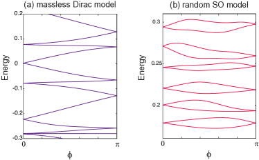
which is now anti-periodic. Here is the coordinate along the wire and parallel to the flux, is the transverse coordinate and is the circumference. The anti-periodicity is a consequence of the fact that the spin lies in the tangent plane to the surface and therefore rotates by an angle of when looping around the surface. Because of the antiperiodic boundary condition the spectrum is gapped as schematically shown in figure 14. Within the same approximation, the effect of applying a flux along the wire is simply to change the boundary condition by the Aharanov-Bohm phase
| (35) |
A flux of half a flux quantum, , cancels the Berry phase and the spectrum becomes gapless (figure 14). Crucially, the number of modes is now odd and there is necessarily at least one perfectly transmitted mode with conductance .
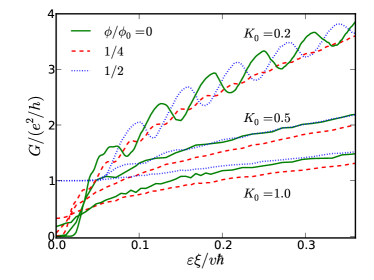
Figure 15 shows the conductance as a function of doping as obtained by a numerical simulation.Bardarson et al. (2010) The simulation includes a Gaussian disorder potential that satisfies . is a dimensionless measure of the disorder strength and is the length scale characterizing the disorder (typical size of electron-hole puddles). For each value of the conductance is given at three values of the flux, which determine the period of possible oscillations. Three different regimes are observed: i) If disorder is large enough such that transport is diffusive the AAS oscillations dominate. The conductance is the same at and . ii) At the Dirac point conductance is dominated by the perfectly transmitted mode. The conductance oscillates with a period of and has a minimum at zero flux. iii) At weak disorder and large enough doping, such that the conductance is no longer dominated by the perfectly transmitted mode, the conductance oscillates with a period of . In this regime the conductance can have either a maximum or a minimum at zero flux, depending on the doping level. The conductance oscillates as a function of doping with a period equal to the level spacing . These oscillations are smeared by temperature when and the conductance at and is equal. The conductance then oscillates with a period of .
IV.2.2 Experimental observations of Aharonov-Bohm oscillations
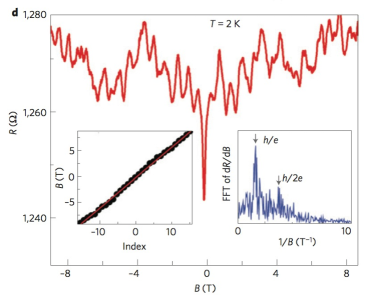
Aharonov-Bohm oscillations have been experimentally observed in nanowires (ribbons, plates) of Bi2Se3,Peng et al. (2009) Bi2Te3,Xiu et al. (2011); Li et al. (2012) and -Ag2Te.Sulaev et al. Related periodic oscillations have also been observed in arrays of ringlike structures.Qu et al. (2011) In the wires, the magnetoconductance shows periodic oscillations superimposed on the UCF (see figure 16 for example data). Fourier transform reveals a strong period and a weaker period.
All the samples are doped away from the Dirac point which in Bi2Te3 is buried in the valence band. In Ref. Xiu et al., 2011 a back gate was used to tune the Fermi level and reduce the bulk contribution to the conductance. The AB oscillations become more pronounced as the surface contribution is enhanced. If these observations are to be consistent with the theory of the last section, the samples would need to be in the weak disorder limit. As a necessary condition the mean level spacing must be large compared to the temperature broadening. From the circumference of the samples one estimates while the measurement temperature is usually . In Ref. Li et al., 2012 a crossover from to oscillations is observed at for a sample with .
In the weak disorder regime the conductance at zero flux will be either maximum or minimum depending on the sample. In Refs. Peng et al., 2009; Xiu et al., 2011; Sulaev et al., the conductance has a maximum while in Ref. Li et al., 2012 it has a minimum. A change in the sign of the magnetoconductance with varying gate voltage was not observed,Xiu et al. (2011) though a systematic exploration of this effect was not undertaken. A clear “smoking gun” signature of Dirac fermion transport in this regime would be the observation of the gate voltage oscillations accompanied by a shift in the magnetoconductance.
Taken together these results are consistent with the theory of doped and weakly disordered TI wires. A more systematic exploration of doping and disorder strength dependence of the AB oscillations is needed to firmly confirm this picture. In particular, the robust oscillations at the Dirac point and the accompanying indirect measurement of the Berry phase is still to be observed.
V Related problems and future directions
We end this review by briefly exploring a couple of related topics. These are quantum transport in WTI and the Josephson effect in TI surfaces.
V.1 Transport at the surface of a weak topological insulator
So far we have mainly focused on the transport properties of strong topological insulators (denoted in this section with STI to clearly differentiate them from the WTI). STI’s have an odd number of Dirac cones at their surface, while weak TI’s have an even number of Dirac cones. A WTI may be realized e.g. in layered semiconductors, such as KHgSb.Yan et al. Topological crystalline insulators which surface electronic structure is also described by an even number of Dirac cones, have recently been proposedFu (2011); Hsieh et al. (2012) and observed.Dziawa et al. ; Xu et al. ; Tanaka et al. In addition a thin film of STI can be considered to be a WTI.
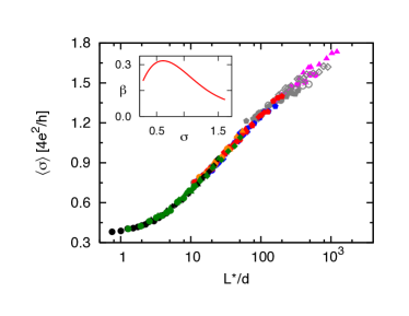
A WTI can be thought of as being obtained by stacking 2D QSHE layers. The helical edges states of the QSHE couple together to form the surface state of the WTI. By construction this surface state will not be found on every face of the sample. If the number of layers is odd the number of propagating modes in the surface is also odd and the surface hosts a perfectly transmitted mode. The conductance is at least and the surface can not localize. The energy levels have a similar switching behavior as in STI.Ringel et al. (2012) Instead of localization the surface of a WTI flows, under rather general conditions to be discussed below, into the symplectic metal.Mong et al. (2012) In this sense the WTI behaves very much like an STI. The effect of interactions on WTI surface states was studied in Ref. Liu et al., 2012c.
The surface state of a WTI can be modeled by two Dirac cones
| (36) |
Here is the momentum operator and the Pauli matrices and act in spin and valley space respectively. The disorder potential can be written as
| (37) |
Of all the possible terms, only and with do not break the time-reversal symmetry which is given by with the complex conjugate, and satisfies . Of these, only opens up a gap in the energy spectrum and we therefore refer to the average of this term as the mass . The disorder terms are independently distributed with where .
For a random potential the mass is zero. A nonzero mass requires the surface potential to be commensurate with an even number of unit cells, and is therefore necessarily zero for an odd number of layers. In this way the mass of the 2D theory connects with the even-odd argument above. Indeed, in the absence of mass disorder drives the surface state into the symplectic metal following a single parameter scaling.Mong et al. (2012) Figure 17 shows the result of a numerical simulation of (36) for various disorder strengths and doping levels including the Dirac point. The system size, horizontal axis, has been scaled by the mean free path to reveal a collapse of the raw data (inset) onto the scaling curve. At large system sizes the conductivity follows the logarithmic dependence of the WAL (19) with a slope of , just as in an STI. This is expected since the two Dirac cones are strongly mixed by the disorder and was verified with an explicit diagrammatic calculation in Ref. Ringel et al., 2012. Note that while the WTI is similar to graphene in the sense that both systems have two Dirac cones, they differ in the sign of the square of the time-reversal operator. For a WTI but for graphene . Intervalley coupling in graphene therefore leads to weak localizationMcCann et al. (2006) and eventually localization.Aleiner and Efetov (2006)
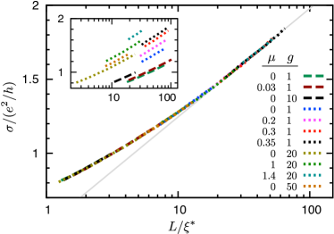
If is nonzero, the surface can be localized by disorder. A metal insulator transition is obtained at a conductivity , just as in a regular spin-orbit coupled 2DEG.Markoš and Schweitzer (2006); Evers and Mirlin (2008) The conductance distribution at the transition is also the same as in the 2DEG.Evers and Mirlin (2008) This is consistent with the two systems being described by the same effective field theory of diffusion, the symplectic NLM in the absence of a topological term.Ryu et al. (2012) The fact that localization is avoided at suggest that the full scaling flow may be described by a two parameter scaling, as in the quantum Hall effectHuckestein (1995). This possibility has been explored in Ref. Mong et al., 2012. If the disorder becomes strong enough that nonlinear in momentum terms need to be added to the Dirac theory (36) localization is expected.
The NLM of a WTI does not have the topological term that protects the STI from localization.Ryu et al. (2012) However, it has recently been argued that for localization to happen, a proliferation of vortex like topological defects in the field configurations is necessary.Fu and Kane Such vortex proliferation is forbidden by average discrete symmetries which are equivalent to having a zero mass, consistent with the observed absence of localization.
V.2 Superconductivity and topological insulators
Another exciting direction that merits a review article of its own is how the proximity effect from a conventional -wave superconductor has unusual effects on topological insulators and related electronic structures such as strongly spin-orbit coupled semiconductors in a magnetic field. Here we mention only some aspects of this problem that relate to the discussion above of the Aharonov-Bohm effect. In a non-superconducting nanowire made from a topological insulator, there is a protected mode when one half of a flux quantum pierces the nanowire.Rosenberg et al. (2010); Ostrovsky et al. (2010) The same metallic mode is there in the inverse problem where space is filled by a 3D topological insulator that has a cylindrical hole in it, pierced by one half of a flux quantum. What happens to this system when the 3D topological insulator is driven superconducting? One half of a flux quantum is of course the magnetic flux associated with an elementary vortex in a charge- superconductor, so the setup is quite natural.
The answer is that the metallic mode becomes gapped along the length of the vortex, but there are zero-energy Majorana excitations at the two ends of the vortexCook and Franz (2011); Hosur et al. (2011); Chiu et al. (2011); Cook et al. (i.e., where it leaves the topological insulator). Their emergence in this system can be understood in two ways. Looking at the surface state of the topological insulator, the proximity effect converts the single-sheet Fermi surface into a “topological superconductor” with one Majorana fermion excitation in each vortex core.Sato (2003); Fu and Kane (2008) An ordinary spinless fermion excitation can be broken up into two Majorana fermions, which are their own Hermitian conjugates. This topological superconducting layer is like a time-reversal symmetric version of the 2D “p+ip” superconductor known to support Majorana fermions in vortex cores.Read and Green (2000) An alternate picture of where the Majorana fermions come from is as tail states of the gapped vortex core.Kitaev (2007) For recent reviews on realizations of Majorana modes in condensed matter systems, see Refs. Alicea, 2012; Beenakker, .
As a first step in the direction towards the observation of the Majorana mode, and of intrinsic interest by itself, proximity effect and a Josephson current through TI surfaces has been demonstrated.Zhang et al. (2011b); Veldhorst et al. (2012a, b); Williams et al. (2012); Yang et al. (2012, ) Both Shapiro steps in the presence of microwave irradiationVeldhorst et al. (2012b) and Fraunhofer interference pattern induced by a magnetic fieldVeldhorst et al. (2012a); Williams et al. (2012) have been observed. The temperature dependence of the data in Ref. Veldhorst et al., 2012b was more consistent with ballistic transport than diffusive transport, and the supercurrent was found to be mainly carried by the surface state, even if the normal state transport was heavily influenced by the bulk states. This servers as an additional motivation for Josephson physics as a probe of the unique properties of the normal state physics which is the focus of this article. In addition, not all aspects of the observed data are fully understoodWilliams et al. (2012) which should spur on further theoretical and experimental efforts in this line of work.
VI Summary
In this report we have reviewed recent theoretical and experimental progress towards the verification of Dirac fermion surface states in topological insulators, through various magnetotransport effects. We have adapted a positive outlook on the status of the field. While there is certainly a significant number of transport experiments that show no reliable signs of surface transport for various reasons, the evidence for Dirac fermion transport and the accompanying Berry phase is mounting. Material improvements are rapid and the first steps in combining TI’s with superconductors are being taken. TI transport therfore has the promise to be fertile grounds for exploring and realizing interesting physics.
At the theoretical level, many of the transport properties of TI surfaces result from disorder driving it into the symplectic metal phase. The symplectic metal is characterized for example by weak anti-localization. However, since this phase is also realized in traditional two dimensional electron gas in the presence of spin-orbit coupling, the nontrivial Berry phase of the Dirac fermion is not easily realized in this limit. The Berry phase is revealed in principle in quantum oscillations such as Shubnikov-de Haas oscillations and, in TI nanowires, Aharonov-Bohm oscillations. We have discussed these effects in detail in the main text.
Signatures of surface transport in large bulk crystals are weak if not absent. This is due to significant bulk conduction, coming from unavoidable bulk doping. Instead, the most convincing data is obtained in thin films, where the surface can have a significant contribution to the total conductivity. Observation of weak anti-localization fitting that expected from the symplectic metal, and 2D SdH oscillations strongly suggest surface transport, though one should keep in mind that the bulk of thin films is often effectively 2D also. Comparison between theory, taking into account the bulk, and experiments suggests the presence of at least two transport channels, bulk and surface. Aharonov-Bohm oscillations have been observed in TI nanowires. These oscillations can in principle reveal the presence of the Berry phase, but this has not been attained with current data. SdH oscillations are in most cases consistent with a nontrivial Berry phase, though the data can be difficult to interpret due to various correction. Finally, the experimentally observed temperature dependence of WAL is seemingly inconsistent with the symplectic metal, possibly pointing towards important effects of electron-electron interactions.
In this review we have focused on the surface theory and mostly ignored the bulk. This reflects our view that eventually insulating bulks will be realized, and that the surface transport contains the more fundamental physics. Lastly, we mention that in addition to the reviews already cited in the introduction,Hasan and Kane (2010); Moore (2010); Qi and Zhang (2011); Hasan and Moore (2011) a couple of focused reviews have appeared recentlyCulcer (2012); Tkachov and Hankiewicz which discuss transport of TI’s from a different perspective.
Acknowledgments
We gratefully acknowledge all our collaborators on the subject of transport in topological insulators, in particular C. W. J. Beenakker, P. W. Brouwer, and R. S. K. Mong. The authors were supported by the LBNL Thermoelectrics Program of DOE BES and the DARPA TI (UCLA) program (JHB) and by NSF DMR-1206515 (JEM).
References
- Hasan and Kane (2010) M. Hasan and C. Kane, Rev. Mod. Phys. 82, 3045 (2010).
- Moore (2010) J. E. Moore, Nature 464, 194 (2010).
- Qi and Zhang (2011) X.-L. Qi and S.-C. Zhang, Rev. Mod. Phys. 83, 1057 (2011).
- Hasan and Moore (2011) M. Z. Hasan and J. E. Moore, Annu. Rev. Condens. Matter Phys. 2, 55 (2011).
- Aharonov and Bohm (1959) Y. Aharonov and D. Bohm, Phys. Rev. 115, 485 (1959).
- Aronov and Sharvin (1987) A. Aronov and Y. Sharvin, Rev. Mod. Phys. 59, 755 (1987).
- Batelaan and Tonomura (2009) H. Batelaan and A. Tonomura, Phys. Today 62, 38 (2009).
- Ando (1982) T. Ando, Rev. Mod. Phys. 54, 437 (1982).
- Castro Neto et al. (2009) A. H. Castro Neto, N. M. R. Peres, K. S. Novoselov, and A. K. Geim, Rev. Mod. Phys. 81, 109 (2009).
- Das Sarma et al. (2011) S. Das Sarma, S. Adam, E. Hwang, and E. Rossi, Rev. Mod. Phys. 83, 407 (2011).
- Bergmann (1984) G. Bergmann, Phys. Rep. 107, 1 (1984).
- Lee and Ramakrishnan (1985) P. A. Lee and T. V. Ramakrishnan, Rev. Mod. Phys. 57, 287 (1985).
- Evers and Mirlin (2008) F. Evers and A. Mirlin, Rev. Mod. Phys. 80, 1355 (2008).
- König et al. (2008) M. König, H. Buhmann, L. W. Molenkamp, T. Hughes, C.-X. Liu, X.-L. Qi, and S.-C. Zhang, J. Phys. Soc. Jpn. 77, 031007 (2008).
- König et al. (2007) M. König, S. Wiedmann, C. Brüne, A. Roth, H. Buhmann, L. W. Molenkamp, X. L. Qi, and S. C. Zhang, Science 318, 766 (2007).
- Nielsen and Ninomiya (1981a) H. B. Nielsen and M. Ninomiya, Nucl. Phys. B 185, 20 (1981a).
- Nielsen and Ninomiya (1981b) H. B. Nielsen and M. Ninomiya, Phys. Lett. B 105, 219 (1981b).
- Fu (2009) L. Fu, Phys. Rev. Lett. 103 (2009).
- Alpichshev et al. (2010) Z. Alpichshev, J. G. Analytis, J. H. Chu, I. R. Fisher, Y. L. Chen, Z. X. Shen, A. Fang, and A. Kapitulnik, Phys. Rev. Lett. 104, 016401 (2010).
- Kuroda et al. (2010) K. Kuroda, M. Arita, K. Miyamoto, M. Ye, J. Jiang, A. Kimura, E. Krasovskii, E. Chulkov, H. Iwasawa, T. Okuda, K. Shimada, Y. Ueda, H. Namatame, and M. Taniguchi, Phys. Rev. Lett. 105, 076802 (2010).
- Yazyev et al. (2010) O. Yazyev, J. E. Moore, and S. Louie, Phys. Rev. Lett. 105, 266806 (2010).
- Pan et al. (2011) Z. H. Pan, E. Vescovo, A. Fedorov, D. Gardner, Y. Lee, S. Chu, G. Gu, and T. Valla, Phys. Rev. Lett. 106, 257004 (2011).
- Souma et al. (2011) S. Souma, K. Kosaka, T. Sato, M. Komatsu, A. Takayama, T. Takahashi, M. Kriener, K. Segawa, and Y. Ando, Phys. Rev. Lett. 106, 216803 (2011).
- (24) K. Okamoto, K. Kuroda, H. Miyahara, K. Miyamoto, T. Okuda, Z. S. Aliev, M. B. Babanly, I. R. Amiraslanov, K. Shimada, H. Namatame, M. Taniguchi, E. V. Chulkov, and A. Kimura, arXiv:1207.2088v1 .
- Hsieh et al. (2008) D. Hsieh, D. Qian, L. Wray, Y. Xia, Y. S. Hor, R. J. Cava, and M. Z. Hasan, Nature 452, 970 (2008).
- Shan et al. (2010) W.-Y. Shan, H.-Z. Lu, and S.-Q. Shen, New J. Phys. 12, 043048 (2010).
- Culcer et al. (2010) D. Culcer, E. Hwang, T. Stanescu, and S. Das Sarma, Phys. Rev. B 82, 155457 (2010).
- Silvestrov et al. (2012) P. Silvestrov, P. Brouwer, and E. Mishchenko, Phys. Rev. B 86, 075302 (2012).
- Zhang et al. (2012) F. Zhang, C. Kane, and E. Mele, Phys. Rev. B 86, 081303 (2012).
- Zhang et al. (a) F. Zhang, C. L. Kane, and E. J. Mele, arXiv:1208.2968v1 .
- Winkler (2003) R. Winkler, Spin-Orbit Coupling Effects in Two-Dimensional Electron and Hole Systems (Springer, 2003).
- Moore and Balents (2007) J. E. Moore and L. Balents, Phys. Rev. B 75, 121306(R) (2007).
- Fu et al. (2007) L. Fu, C. Kane, and E. Mele, Phys. Rev. Lett. 98, 106803 (2007).
- Roy (2009) R. Roy, Phys. Rev. B 79, 195322 (2009).
- Suzuura and Ando (2002) H. Suzuura and T. Ando, Phys. Rev. Lett. 89, 266603 (2002).
- Schmidt et al. (2012) T. Schmidt, S. Rachel, F. von Oppen, and L. Glazman, Phys. Rev. Lett. 108, 156402 (2012).
- Roushan et al. (2009) P. Roushan, J. Seo, C. V. Parker, Y. S. Hor, D. Hsieh, D. Qian, A. Richardella, M. Z. Hasan, R. J. Cava, and A. Yazdani, Nature 460, 1106 (2009).
- Knez et al. (2011) I. Knez, R.-R. Du, and G. Sullivan, Phys. Rev. Lett. 107, 136603 (2011).
- Weeks et al. (2011) C. Weeks, J. Hu, J. Alicea, M. Franz, and R. Wu, Phys. Rev. X 1, 021001 (2011).
- (40) J. Hu, J. Alicea, R. Wu, and M. Franz, arXiv:1206.4320v1 .
- Abanin and Pesin (2012) D. Abanin and D. Pesin, Phys. Rev. Lett. 109, 066802 (2012).
- Zhang et al. (2009a) H. Zhang, C.-X. Liu, X.-L. Qi, X. Dai, Z. Fang, and S.-C. Zhang, Nat. Phys. 5, 438 (2009a).
- (43) T. Valla, H. Ji, L. M. Schoop, A. P. Weber, Z. H. Pan, J. T. Sadowski, E. Vescovo, A. V. Fedorov, A. N. Caruso, Q. D. Gibson, L. M uchler, C. Felser, and R. J. Cava, arXiv:1208.2741v1 .
- Xia et al. (2009) Y. Xia, D. Qian, D. Hsieh, L. Wray, A. Pal, H. Lin, A. Bansil, D. Grauer, Y. S. Hor, R. J. Cava, and M. Z. Hasan, Nat. Phys. 5, 398 (2009).
- Yazyev et al. (2012) O. Yazyev, E. Kioupakis, J. E. Moore, and S. Louie, Phys. Rev. B 85, 161101 (2012).
- Chen et al. (2009) Y. L. Chen, J. G. Analytis, J. H. Chu, Z. K. Liu, S. K. Mo, X. L. Qi, H. J. Zhang, D. H. Lu, X. Dai, Z. Fang, S. C. Zhang, I. R. Fisher, Z. Hussain, and Z. X. Shen, Science 325, 178 (2009).
- Jia et al. (2011) S. Jia, H. Ji, E. Climent-Pascual, M. Fuccillo, M. Charles, J. Xiong, N. Ong, and R. Cava, Phys. Rev. B 84, 235206 (2011).
- Xiong et al. (2012a) J. Xiong, Y. Luo, Y. Khoo, S. Jia, R. Cava, and N. Ong, Phys. Rev. B 86, 045314 (2012a).
- Mong et al. (2010) R. Mong, A. Essin, and J. E. Moore, Phys. Rev. B 81, 245209 (2010).
- Fu and Berg (2010) L. Fu and E. Berg, Phys. Rev. Lett. 105, 097001 (2010).
- Brüne et al. (2011) C. Brüne, C. Liu, E. Novik, E. Hankiewicz, H. Buhmann, Y. Chen, X. Qi, Z. Shen, S. Zhang, and L. Molenkamp, Phys. Rev. Lett. 106, 126803 (2011).
- Zhang et al. (2011a) W. Zhang, R. Yu, W. Feng, Y. Yao, H. Weng, X. Dai, and Z. Fang, Phys. Rev. Lett. 106, 156808 (2011a).
- (53) A. Sulaev, P. Ren, B. Xia, Q. H. Lin, T. Yu, C. Qiu, S.-Y. Zhang, M.-Y. Han, Z. P. Li, W. G. Zhu, Q. Wu, Y. P. Feng, L. Shen, S.-Q. Shen, and L. Wang, arXiv:1204.3816v5 .
- Linder et al. (2009) J. Linder, T. Yokoyama, and A. Sudbø, Phys. Rev. B 80, 205401 (2009).
- Liu et al. (2010) C.-X. Liu, H. Zhang, B. Yan, X.-L. Qi, T. Frauenheim, X. Dai, Z. Fang, and S.-C. Zhang, Phys. Rev. B 81, 041307 (2010).
- Lu et al. (2010) H.-Z. Lu, W.-Y. Shan, W. Yao, Q. Niu, and S.-Q. Shen, Phys. Rev. B 81, 115407 (2010).
- Zhang et al. (2009b) T. Zhang, P. Cheng, X. Chen, J.-F. Jia, X. Ma, K. He, L. Wang, H. Zhang, X. Dai, Z. Fang, X. Xie, and Q.-K. Xue, Phys. Rev. Lett. 103, 266803 (2009b).
- Liu et al. (2012a) Y. Liu, G. Bian, T. Miller, M. Bissen, and T. C. Chiang, Phys. Rev. B 85, 195442 (2012a).
- Zhang et al. (2010) Y. Zhang, K. He, C.-Z. Chang, C.-L. Song, L.-l. Wang, X. Chen, J.-F. Jia, Z. Fang, X. Dai, W.-Y. Shan, S.-Q. Shen, Q. Niu, X.-L. Qi, S.-C. Zhang, X.-C. Ma, and Q.-K. Xue, Nat. Phys. 6, 584 (2010).
- Cho et al. (2011) S. Cho, N. P. Butch, J. Paglione, and M. S. Fuhrer, Nano Lett. 11, 1925 (2011).
- Cho et al. (2012) S. Cho, D. Kim, P. Syers, N. P. Butch, J. Paglione, and M. S. Fuhrer, Nano Lett. 12, 469 (2012).
- Taskin et al. (2012) A. Taskin, S. Sasaki, K. Segawa, and Y. Ando, Phys. Rev. Lett. 109, 066803 (2012).
- Analytis et al. (2010a) J. G. Analytis, R. D. McDonald, S. C. Riggs, J.-H. Chu, G. S. Boebinger, and I. R. Fisher, Nat. Phys. 6, 960 (2010a).
- Eisenstein and MacDonald (2004) J. P. Eisenstein and A. H. MacDonald, Nat. Phys. 432, 691 (2004).
- Altland and Zirnbauer (1997) A. Altland and M. R. Zirnbauer, Phys. Rev. B 55, 1142 (1997).
- Ando et al. (1998) T. Ando, T. Nakanishi, and R. Saito, J. Phys. Soc. Jpn. 67, 2857 (1998).
- Ando and Suzuura (2002) T. Ando and H. Suzuura, J. Phys. Soc. Jpn. 71, 2753 (2002).
- Bardarson (2008) J. H. Bardarson, J. Phys. A: Math. Theor. 41, 405203 (2008).
- Tworzydło et al. (2006) J. Tworzydło, B. Trauzettel, M. Titov, A. Rycerz, and C. W. J. Beenakker, Phys. Rev. Lett. 96, 246802 (2006).
- Beenakker (1997) C. W. J. Beenakker, Rev. Mod. Phys. 69, 731 (1997).
- Akkermans and Montambaux (2007) E. Akkermans and G. Montambaux, Mesoscopic Physics of Electrons and Photons (Cambridge University Press, 2007).
- Hikami et al. (1980) S. Hikami, A. I. Larkin, and Y. Nagaoka, Prog. Theor. Phys. 63, 707 (1980).
- Bergmann (1983) G. Bergmann, Phys. Rev. B 28, 2914 (1983).
- McCann et al. (2006) E. McCann, K. Kechedzhi, V. I. Fal’ko, H. Suzuura, T. Ando, and B. L. Altshuler, Phys. Rev. Lett. 97, 146805 (2006).
- Imura et al. (2009) K.-I. Imura, Y. Kuramoto, and K. Nomura, Phys. Rev. B 80, 085119 (2009).
- Tkachov and Hankiewicz (2011) G. Tkachov and E. M. Hankiewicz, Phys. Rev. B 84, 035444 (2011).
- Lu et al. (2011) H.-Z. Lu, J. Shi, and S.-Q. Shen, Phys. Rev. Lett. 107, 076801 (2011).
- Lu and Shen (2011) H.-Z. Lu and S.-Q. Shen, Phys. Rev. B 84, 125138 (2011).
- Garate and Glazman (2012) I. Garate and L. Glazman, Phys. Rev. B 86, 035422 (2012).
- (80) P. Adroguer, D. Carpentier, J. Cayssol, and E. Orignac, arXiv:1205.5209v1 .
- (81) V. Krueckl and K. Richter, arXiv:1207.1294v1 .
- Gutzwiller (1990) M. C. Gutzwiller, Chaos in Classical and Quantum Mechanics (Springer, 1990).
- Haake (2010) F. Haake, Quantum Signatures of Chaos, 3rd ed. (Springer, 2010).
- Zaitsev et al. (2005) O. Zaitsev, D. Frustaglia, and K. Richter, Phys. Rev. B 72, 155325 (2005).
- Aleiner and Larkin (1996) I. Aleiner and A. Larkin, Phys. Rev. B 54, 14423 (1996).
- Richter and Sieber (2002) K. Richter and M. Sieber, Phys. Rev. Lett. 89, 206801 (2002).
- Müller et al. (2007) S. Müller, S. Heusler, P. Braun, and F. Haake, New J. Phys. 9, 12 (2007).
- Altshuler et al. (1981) B. L. Altshuler, A. G. Aronov, and B. Z. Spivak, JETP Lett. 33, 94 (1981).
- Sharvin and Sharvin (1981) D. Y. Sharvin and Y. V. Sharvin, JETP Lett. 34, 272 (1981).
- Cheianov et al. (2007) V. V. Cheianov, V. I. Fal’ko, B. L. Altshuler, and I. L. Aleiner, Phys. Rev. Lett. 99, 176801 (2007).
- Rycerz et al. (2007) A. Rycerz, J. Tworzydło, and C. W. J. Beenakker, EPL 79, 57003 (2007).
- Kechedzhi et al. (2008) K. Kechedzhi, O. Kashuba, and V. Fal’ko, Phys. Rev. B 77, 193403 (2008).
- Kharitonov and Efetov (2008) M. Kharitonov and K. Efetov, Phys. Rev. B 78, 033404 (2008).
- Rossi et al. (2012) E. Rossi, J. H. Bardarson, M. S. Fuhrer, and S. Das Sarma, Phys. Rev. Lett. 109, 096801 (2012).
- Checkelsky et al. (2011) J. Checkelsky, Y. Hor, R. Cava, and N. Ong, Phys. Rev. Lett. 106, 196801 (2011).
- Matsuo et al. (2012) S. Matsuo, T. Koyama, K. Shimamura, T. Arakawa, Y. Nishihara, D. Chiba, K. Kobayashi, T. Ono, C.-Z. Chang, K. He, X.-C. Ma, and Q.-K. Xue, Phys. Rev. B 85, 075440 (2012).
- (97) Z. Li, T. Chen, H. Pan, F. Song, B. Wang, J. Han, Y. Qin, X. Wang, R. Zhang, J. Wan, D. Xing, and G. Wang, arXiv:1207.2260v1 .
- Checkelsky et al. (2009) J. Checkelsky, Y. Hor, M. H. Liu, D. X. Qu, R. Cava, and N. Ong, Phys. Rev. Lett. 103, 246601 (2009).
- Efetov (1997) K. Efetov, Supersymmetry in Disorder and Chaos (Cambridge University Press, 1997).
- Hikami (1981) S. Hikami, Phys. Rev. B 24, 2671 (1981).
- Hikami (1992) S. Hikami, Prog. Theor. Phys. Suppl. 107, 213 (1992).
- Kim et al. (2012) D. Kim, S. Cho, N. P. Butch, P. Syers, K. Kirshenbaum, S. Adam, J. Paglione, and M. S. Fuhrer, Nat. Phys. 8, 460 (2012).
- Steinberg et al. (2010) H. Steinberg, D. R. Gardner, Y. S. Lee, and P. Jarillo-Herrero, Nano Lett. 10, 5032 (2010).
- Ren et al. (2011) Z. Ren, A. Taskin, S. Sasaki, K. Segawa, and Y. Ando, Phys. Rev. B 84, 075316 (2011).
- Kong et al. (2011) D. Kong, Y. Chen, J. J. Cha, Q. Zhang, J. G. Analytis, K. Lai, Z. Liu, S. S. Hong, K. J. Koski, S.-K. Mo, Z. Hussain, I. R. Fisher, Z.-X. Shen, and Y. Cui, Nat. Nanotechnol. 6, 705 (2011).
- Sacépé et al. (2011) B. Sacépé, J. B. Oostinga, J. Li, A. Ubaldini, N. J. G. Couto, E. Giannini, and A. F. Morpurgo, Nat. Commun. 2, 575 (2011).
- Hao et al. (2012) G. Hao, X. Qi, Y. Liu, Z. Huang, H. Li, K. Huang, J. Li, L. Yang, and J. Zhong, J. Appl. Phys. 111, 114312 (2012).
- Adam et al. (2012) S. Adam, E. Hwang, and S. Das Sarma, Phys. Rev. B 85, 235413 (2012).
- Beidenkopf et al. (2011) H. Beidenkopf, P. Roushan, J. Seo, L. Gorman, I. Drozdov, Y. S. Hor, R. J. Cava, and A. Yazdani, Nat. Phys. 7, 939 (2011).
- Bardarson et al. (2007) J. H. Bardarson, J. Tworzydło, P. W. Brouwer, and C. W. J. Beenakker, Phys. Rev. Lett. 99, 106801 (2007).
- Fu and Kane (2007) L. Fu and C. Kane, Phys. Rev. B 76, 045302 (2007).
- Ryu et al. (2007) S. Ryu, C. Mudry, H. Obuse, and A. Furusaki, Phys. Rev. Lett. 99, 116601 (2007).
- Ostrovsky et al. (2007) P. Ostrovsky, I. Gornyi, and A. Mirlin, Phys. Rev. Lett. 98, 256801 (2007).
- Nomura et al. (2007) K. Nomura, M. Koshino, and S. Ryu, Phys. Rev. Lett. 99, 146806 (2007).
- Markoš and Schweitzer (2006) P. Markoš and L. Schweitzer, J. Phys. A: Math. Gen. 39, 3221 (2006).
- Schnyder et al. (2008) A. Schnyder, S. Ryu, A. Furusaki, and A. Ludwig, Phys. Rev. B 78, 195125 (2008).
- Biswas and Balatsky (2010) R. Biswas and A. Balatsky, Phys. Rev. B 81, 233405 (2010).
- Black-Schaffer and Balatsky (2012) A. Black-Schaffer and A. Balatsky, Phys. Rev. B 85, 121103 (2012).
- Alpichshev et al. (2012) Z. Alpichshev, R. Biswas, A. Balatsky, J. Analytis, J. H. Chu, I. Fisher, and A. Kapitulnik, Phys. Rev. Lett. 108, 206402 (2012).
- (120) B. Skinner, T. Chen, and B. I. Shklovskii, arXiv:1208.4601v1 .
- Shoenberg (1984) D. Shoenberg, Magnetic Oscillations in Metals (Cambridge University Press, 1984).
- Mikitik and Sharlai (1999) G. Mikitik and Y. Sharlai, Phys. Rev. Lett. 82, 2147 (1999).
- Mikitik and Sharlai (2012) G. Mikitik and Y. Sharlai, Phys. Rev. B 85, 033301 (2012).
- Ando (1974) T. Ando, J. Phys. Soc. Jpn. 37, 1233 (1974).
- (125) L. Fang, Y. Jia, D. J. Miller, M. L. Latimer, Z. L. Xiao, U. Welp, G. W. Crabtree, and W. K. Kwok, arXiv:1208.4532v1 .
- Lee (2009) D.-H. Lee, Phys. Rev. Lett. 103, 196804 (2009).
- Vafek (2011) O. Vafek, Phys. Rev. B 84, 245417 (2011).
- Sitte et al. (2012) M. Sitte, A. Rosch, E. Altman, and L. Fritz, Phys. Rev. Lett. 108, 126807 (2012).
- Analytis et al. (2010b) J. G. Analytis, J.-H. Chu, Y. Chen, F. Corredor, R. D. McDonald, Z. X. Shen, and I. R. Fisher, Phys. Rev. B 81, 205407 (2010b).
- Eto et al. (2010) K. Eto, Z. Ren, A. A. Taskin, K. Segawa, and Y. Ando, Phys. Rev. B 81, 195309 (2010).
- Butch et al. (2010) N. P. Butch, K. Kirshenbaum, P. Syers, A. B. Sushkov, G. S. Jenkins, H. D. Drew, and J. Paglione, Phys. Rev. B 81, 241301(R) (2010).
- Taskin et al. (2010) A. Taskin, K. Segawa, and Y. Ando, Phys. Rev. B 82, 121302 (2010).
- Qu et al. (2010) D. X. Qu, Y. S. Hor, J. Xiong, R. J. Cava, and N. P. Ong, Science 329, 821 (2010).
- Taskin et al. (2011) A. Taskin, Z. Ren, S. Sasaki, K. Segawa, and Y. Ando, Phys. Rev. Lett. 107, 016801 (2011).
- Ren et al. (2010) Z. Ren, A. Taskin, S. Sasaki, K. Segawa, and Y. Ando, Phys. Rev. B 82, 241306(R) (2010).
- Wang et al. (2012) Y. Wang, F. Xiu, L. Cheng, L. He, M. Lang, J. Tang, X. Kou, X. Yu, X. Jiang, Z. Chen, J. Zou, and K. L. Wang, Nano Lett. 12, 1170 (2012).
- He et al. (2012) L. He, F. Xiu, X. Yu, M. Teague, W. Jiang, Y. Fan, X. Kou, M. Lang, Y. Wang, G. Huang, N.-C. Yeh, and K. L. Wang, Nano Lett. 12, 1486 (2012).
- Xiong et al. (2012b) J. Xiong, A. C. Petersen, D. Qu, Y. S. Hor, R. J. Cava, and N. P. Ong, Physica E 44, 917 (2012b).
- Petrushevsky et al. (2012) M. Petrushevsky, E. Lahoud, A. Ron, E. Maniv, I. Diamant, I. Neder, S. Wiedmann, V. Guduru, F. Chiappini, U. Zeitler, J. Maan, K. Chashka, A. Kanigel, and Y. Dagan, Phys. Rev. B 86, 045131 (2012).
- Taskin and Ando (2011) A. Taskin and Y. Ando, Phys. Rev. B 84, 035301 (2011).
- Cheng et al. (2010) P. Cheng, C. Song, T. Zhang, Y. Zhang, Y. Wang, J.-F. Jia, J. Wang, Y. Wang, B.-F. Zhu, X. Chen, X. Ma, K. He, L. Wang, X. Dai, Z. Fang, X. Xie, X.-L. Qi, C.-X. Liu, S.-C. Zhang, and Q.-K. Xue, Phys. Rev. Lett. 105, 076801 (2010).
- Hanaguri et al. (2010) T. Hanaguri, K. Igarashi, M. Kawamura, H. Takagi, and T. Sasagawa, Phys. Rev. B 82, 081305 (2010).
- Cao et al. (2012) H. Cao, J. Tian, I. Miotkowski, T. Shen, J. Hu, S. Qiao, and Y. Chen, Phys. Rev. Lett. 108, 216803 (2012).
- Taskin and Ando (2009) A. Taskin and Y. Ando, Phys. Rev. B 80, 085303 (2009).
- Kim et al. (2011a) H.-J. Kim, K.-S. Kim, M. D. Kim, S. J. Lee, J. W. Han, A. Ohnishi, M. Kitaura, M. Sasaki, A. Kondo, and K. Kindo, Phys. Rev. B 84, 125144 (2011a).
- (146) B. J. Lawson, Y. S. Hor, and L. Li, arXiv:1207.0267v1 .
- Hirahara et al. (2010) T. Hirahara, Y. Sakamoto, Y. Takeichi, H. Miyazaki, S.-i. Kimura, I. Matsuda, A. Kakizaki, and S. Hasegawa, Phys. Rev. B 82, 155309 (2010).
- Chen et al. (2010) J. Chen, H. Qin, F. Yang, J. Liu, T. Guan, F. Qu, G. Zhang, J. Shi, X. Xie, C. Yang, K. Wu, Y. Li, and L. Lu, Phys. Rev. Lett. 105, 176602 (2010).
- Liu et al. (2011) M. Liu, C.-Z. Chang, Z. Zhang, Y. Zhang, W. Ruan, K. He, L.-l. Wang, X. Chen, J.-F. Jia, S.-C. Zhang, Q.-K. Xue, X. Ma, and Y. Wang, Phys. Rev. B 83, 165440 (2011).
- Chen et al. (2011) J. Chen, X. He, K. Wu, Z. Ji, L. Lu, J. Shi, J. Smet, and Y. Li, Phys. Rev. B 83, 241304(R) (2011).
- Wang et al. (2011) J. Wang, A. DaSilva, C.-Z. Chang, K. He, J. Jain, N. Samarth, X.-C. Ma, Q.-K. Xue, and M. Chan, Phys. Rev. B 83, 245438 (2011).
- Kim et al. (2011b) Y. S. Kim, M. Brahlek, N. Bansal, E. Edrey, G. Kapilevich, K. Iida, M. Tanimura, Y. Horibe, S.-W. Cheong, and S. Oh, Phys. Rev. B 84, 073109 (2011b).
- Steinberg et al. (2011) H. Steinberg, J.-B. Laloe, V. Fatemi, J. S. Moodera, and P. Jarillo-Herrero, Phys. Rev. B 84, 233101 (2011).
- Liu et al. (2012b) M. Liu, J. Zhang, C.-Z. Chang, Z. Zhang, X. Feng, K. Li, K. He, L.-l. Wang, X. Chen, X. Dai, Z. Fang, Q.-K. Xue, X. Ma, and Y. Wang, Phys. Rev. Lett. 108, 036805 (2012b).
- Takagaki et al. (2012) Y. Takagaki, B. Jenichen, U. Jahn, M. Ramsteiner, and K. J. Friedland, Phys. Rev. B 85, 115314 (2012).
- Zhang et al. (b) L. Zhang, R. Hammond, M. Dolev, M. Liu, A. Palevski, and A. Kapitulnik, arXiv:1205.5832v1 (b).
- (157) N. Bansal, Y. S. Kim, M. Brahlek, E. Edrey, and S. Oh, arXiv:1104.5709v1 .
- He et al. (2011) H.-T. He, G. Wang, T. Zhang, I.-K. Sou, G. Wong, J.-N. Wang, H.-Z. Lu, S.-Q. Shen, and F.-C. Zhang, Phys. Rev. Lett. 106, 166805 (2011).
- Cha et al. (2012) J. J. Cha, D. Kong, S. S. Hong, J. G. Analytis, K. Lai, and Y. Cui, Nano Lett. 12, 1107 (2012).
- (160) M. Lang, et al. in preparation .
- Altshuler and Aronov (1985) B. L. Altshuler and A. G. Aronov, in Electron-Electron Interactions in Disordered Conductors (Elsevier, New York, 1985) p. 1.
- Pal et al. (2012) H. Pal, V. Yudson, and D. Maslov, Phys. Rev. B 85, 085439 (2012).
- Ostrovsky et al. (2010) P. Ostrovsky, I. Gornyi, and A. Mirlin, Phys. Rev. Lett. 105, 036803 (2010).
- Ran et al. (2008) Y. Ran, A. Vishwanath, and D.-H. Lee, Phys. Rev. Lett. 101, 086801 (2008).
- Rosenberg et al. (2010) G. Rosenberg, H. M. Guo, and M. Franz, Phys. Rev. B 82, 041104(R) (2010).
- Bardarson et al. (2010) J. H. Bardarson, P. W. Brouwer, and J. E. Moore, Phys. Rev. Lett. 105, 156803 (2010).
- Zhang and Vishwanath (2010) Y. Zhang and A. Vishwanath, Phys. Rev. Lett. 105, 206601 (2010).
- Peng et al. (2009) H. Peng, K. Lai, D. Kong, S. Meister, Y. Chen, X.-L. Qi, S.-C. Zhang, Z.-X. Shen, and Y. Cui, Nature Mater. 9, 225 (2009).
- Xiu et al. (2011) F. Xiu, L. He, Y. Wang, L. Cheng, L.-T. Chang, M. Lang, G. Huang, X. Kou, Y. Zhou, X. Jiang, Z. Chen, J. Zou, A. Shailos, and K. L. Wang, Nat. Nanotechnol. 6, 216 (2011).
- Li et al. (2012) Z. Li, Y. Qin, F. Song, Q.-H. Wang, X. Wang, B. Wang, H. Ding, C. Van Haesondonck, J. Wan, Y. Zhang, and G. Wang, Appl. Phys. Lett. 100, 083107 (2012).
- Qu et al. (2011) F. Qu, F. Yang, J. Chen, J. Shen, Y. Ding, J. Lu, Y. Song, H. Yang, G. Liu, J. Fan, Y. Li, Z. Ji, C. Yang, and L. Lu, Phys. Rev. Lett. 107, 016802 (2011).
- (172) B. Yan, L. Muechler, and C. Felser, arXiv:1206.4399v1 .
- Fu (2011) L. Fu, Phys. Rev. Lett. 106, 106802 (2011).
- Hsieh et al. (2012) T. H. Hsieh, H. Lin, J. Liu, W. Duan, A. Bansil, and L. Fu, Nat. Commun. 3, 982 (2012).
- (175) P. Dziawa, B. J. Kowalski, K. Dybko, R. Buczko, A. Szczerbakow, M. Szot, E. Łusakowska, T. Balasubramanian, B. M. Wojek, M. H. Berntsen, O. Tjernberg, and T. Story, arXiv:1206.1705v1 .
- (176) S.-Y. Xu, C. Liu, N. Alidoust, D. Qian, M. Neupane, J. D. Denlinger, Y. J. Wang, L. A. Wray, R. J. Cava, H. Lin, A. Marcinkova, E. Morosan, A. Bansil, and M. Z. Hasan, arXiv:1206.2088v1 .
- (177) Y. Tanaka, Z. Ren, T. Sato, K. Nakayama, S. Souma, T. Takahashi, K. Segawa, and Y. Ando, arXiv:1206.5399v1 .
- Ringel et al. (2012) Z. Ringel, Y. Kraus, and A. Stern, Phys. Rev. B 86, 045102 (2012).
- Mong et al. (2012) R. S. K. Mong, J. H. Bardarson, and J. E. Moore, Phys. Rev. Lett. 108, 076804 (2012).
- Liu et al. (2012c) C.-X. Liu, X.-L. Qi, and S.-C. Zhang, Physica E 44, 906 (2012c).
- Aleiner and Efetov (2006) I. L. Aleiner and K. B. Efetov, Phys. Rev. Lett. 97, 236801 (2006).
- Ryu et al. (2012) S. Ryu, C. Mudry, A. W. W. Ludwig, and A. Furusaki, Phys. Rev. B 85, 235115 (2012).
- Huckestein (1995) B. Huckestein, Rev. Mod. Phys. 67, 357 (1995).
- (184) L. Fu and C. L. Kane, arXiv:1208.3442v1 .
- Cook and Franz (2011) A. Cook and M. Franz, Phys. Rev. B 84, 201105(R) (2011).
- Hosur et al. (2011) P. Hosur, P. Ghaemi, R. Mong, and A. Vishwanath, Phys. Rev. Lett. 107, 097001 (2011).
- Chiu et al. (2011) C.-K. Chiu, M. Gilbert, and T. Hughes, Phys. Rev. B 84, 144507 (2011).
- (188) A. M. Cook, M. M. Vazifeh, and M. Franz, arXiv:1206.3829v1 .
- Sato (2003) M. Sato, Phys. Lett. B 575, 126 (2003).
- Fu and Kane (2008) L. Fu and C. Kane, Phys. Rev. Lett. 100, 096407 (2008).
- Read and Green (2000) N. Read and D. Green, Phys. Rev. B 61, 10267 (2000).
- Kitaev (2007) A. Y. Kitaev, Phys.-Usp. 44, 131 (2007).
- Alicea (2012) J. Alicea, Rep. Prog. Phys. 75, 076501 (2012).
- (194) C. W. J. Beenakker, arXiv:1112.1950v2 .
- Zhang et al. (2011b) D. Zhang, J. Wang, A. DaSilva, J. S. Lee, H. Gutierrez, M. Chan, J. Jain, and N. Samarth, Phys. Rev. B 84, 165120 (2011b).
- Veldhorst et al. (2012a) M. Veldhorst, C. G. Molenaar, X. L. Wang, H. Hilgenkamp, and A. Brinkman, Appl. Phys. Lett. 100, 072602 (2012a).
- Veldhorst et al. (2012b) M. Veldhorst, M. Snelder, M. Hoek, T. Gang, V. K. Guduru, X. L. Wang, U. Zeitler, W. G. van der Wiel, A. A. Golubov, H. Hilgenkamp, and A. Brinkman, Nature Mater. 11, 417 (2012b).
- Williams et al. (2012) J. Williams, A. Bestwick, P. Gallagher, S. Hong, Y. Cui, A. Bleich, J. Analytis, I. Fisher, and D. Goldhaber-Gordon, Phys. Rev. Lett. 109, 056803 (2012).
- Yang et al. (2012) F. Yang, Y. Ding, F. Qu, J. Shen, J. Chen, Z. Wei, Z. Ji, G. Liu, J. Fan, C. Yang, T. Xiang, and L. Lu, Phys. Rev. B 85, 104508 (2012).
- (200) F. Yang, F. Qu, J. Shen, Y. Ding, J. Chen, Z. Ji, G. Liu, J. Fan, C. Yang, L. Fu, and L. Lu, arXiv:1206.6178v1 .
- Culcer (2012) D. Culcer, Physica E 44, 860 (2012).
- (202) G. Tkachov and E. M. Hankiewicz, arXiv:1208.1466v1 .