Exciton radiative decay through plasmon modes in planar metal-semiconductor structures
Abstract
We develop a non-local dielectric response theory to describe the temperature dependence of exciton lifetime in metal-semiconductor heterostructures. Coupling between excitons and surface plasmons results in a strongly nonmonotonous behaviour of exciton radiative decay rate versus temperature. Tuning the plasmon frequency one can control the efficiency of exciton emission of light.
Emission enhancement by placing a light source near the metal surface generally known as the Purcell effect was studied for a wide variety of metal-emitter structures Koenderink (2010); Meinzer et al. (2010); Anger et al. (2006); Kühn et al. (2006); Curto et al. (2010); Ajiki et al. (2002); Glazov et al. (2011). However in the spectral range where the dielectric function of metal exhibits features linked to collective oscillations of electron gas one should take into account the possible energy transfer from excitons to plasmon modes. In this Letter we show that exciton-plasmon coupling may dramatically affect the exciton radiative lifetime and strongly modify the Purcell effect.
Energies of bulk plasmons in typical metals lie in the ultraviolet spectral range ( eV). Introduction of a boundary between metal and dielectric medium results in appearance of a new type of coupled light-electronic modes: surface plasmon-polaritons (SPP) whose resonance frequencies may be found in the near ultraviolet or even optical spectral region. Tuning the SPP frequencies to the vicinity of the band-gap frequency in metal-semiconductor structures allows for coupling of semiconductor emission to the plasmonic modes resulting in a strong modification of the emitter characteristics. Firstly observed for emitting molecules placed near the metal surface Ford and Weber (1984); Chance et al. (1978) this effect is now on topic for the use in solid state physics, especially in gallium-nitride-based light emitting devices, where increasing the light extraction efficiency is one of the major technological challenges. The reduction of exciton lifetime in GaN/InGaN emitters covered by metal layers has been observed experimentally at the beginning of this century Gontijo et al. (1999); Neogi et al. (2002); Okamoto et al. (2004, 2005); Lin et al. (2010). A similar effect has been detected recently in the structures containing metallic nanoparticles Jang et al. (2012); Toropov et al. (2009) and cells Tanaka et al. (2010).
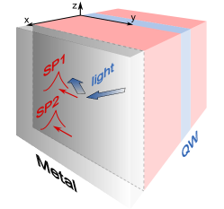
Here by means of a non-local dielectric response theory we describe the temperature dependence of exciton lifetime in planar metal-semiconductor heterostructures. We show that the exciton radiative decay affected by the coupling with surface plasmon modes, experiences a strong nonmonotonous variation with temperature. Tuning the plasmon frequency as well as the exciton level position in a quantum well (either by quantum well width or temperature variation) one can achieve a significant enhancement of the exciton emission efficiency. The structure considered in this paper is schematically shown in Fig. 1. It consists of a quantum well (QW) sandwiched between two barrier layers, one of them covered by a metallic film. In the calculations we use the parameters of InGaN/GaN QWs, which are mostly experimentally relevant, although our model is applicable for a wide variety of materials.
Let us first consider free excitons in a quantum well with a broad thermal distribution of energies (this model is well applicable for light emitting diode devices, where the charge carriers are injected in an active region electrically). The excitons therefore have in-plane wavevectors varying in large limits with the corresponding occupation numbers obeying the Boltzmann statistic. Optical selection rules require conservation of the in-plane wave-vector for light emitted by excitons in QWs. Light emitted by excitons propagates inside the barrier layers and either escapes the system through its boundary or excites one of the plasmon mode or, after a reflection act, comes back to QW and eventually decays in the substrate material. It is well known that only the photons with wavevectors inside the so-called light cone can escape the ideal planar sample. Thus only the excitons with the wavevectors satisfying the condition , where is the light frequency and is the speed of light in vacuum are directly coupled to the continuum of photonic states in vacuum. The decay rate of these excitons depends on the polarisation of light Ivchenko (2005). The heavy-hole excitons in zinc-blende-based semiconductor heterostructures as well as A-excitons in GaN/InGaN systems are optically inactive in polarization Ivchenko (2005), where is the growth direction, so that the corresponding contribution in p-polarized emission vanishes.
The integrated decay rate of the thermal population of excitons in a quantum well can be obtained by simply averaging single exciton decays over all values of . Considering isotropic isoenergetic contours of an exciton in -space and a Boltzmann statistic for the excitons at temperature one can obtain
| (1) |
where is the exciton translation mass, is the Boltzmann constant, and is the Planck constant, , and are radiative decay rates of - and -polarised excitons.
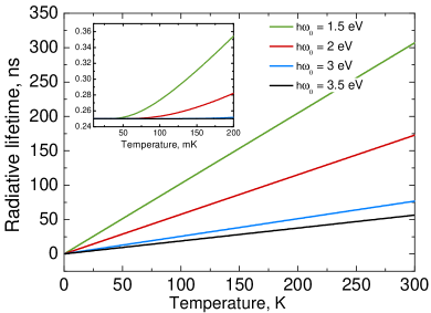
Fig. 2 shows the direct exciton radiative decay rate as a function of temperature. It is seen that a linear behaviour is observed in a range of temperatures where the typical kinetic energy of exciton is much less than the thermal energy . Nonlinear effects become apparent at the temperatures of the order of tens of mK (see the inset).
Surface plasmons propagate along a metal-dielectric interface with wavevectors exceeding , which is why the amplitude of electromagnetic field of a plasmon decays in both directions perpendicular to the metal surface. The dispersion of these modes is given by Pitarke et al. (2007)
| (2) |
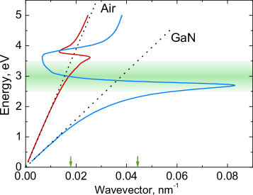
where are dielectric functions of the dielectric (semiconductor) and metal respectively. The frequency dependence of in real metals is quite complicated. has a large imaginary part accounting for the absorption of light in metal. The useful characteristic of a plasmon is the extinction coefficient defined as the imaginary part of effective dielectric function in the right part of Eq. (2). The frequency dependence of the extinction coefficient at the interfaces with air () and GaN ( Sanford et al. (2003)) for aluminum, silver and gold (experimental data on taken from Ehrenreich and Philipp (1962); Ehrenreich et al. (1963); Cooper et al. (1965)) is presented in the lower panel of Fig. 1. For the ease of comparison, the range of exciton energies in InGaN with indium concentration varying from 0 to 0.3 is shown in green. One can see that the most effective plasmon generation on the both interfaces can be performed with the use of aluminum layer, but its plasmon peak is quite far from the attractive range of frequencies. The gold peak is close to that range, but the losses are too large to provide an effective coupling, so we stop at the silver coating and use its parameters for the following simulations. The dispersion curves of silver SPP’s calculated for the dielectric functions extracted from the experimental data are presented in Fig. 3. The plasmon peak for silver approaches the exciton frequency in panel (a) corresponding to the realistic GaN/metal interface.
The fundamental property of a smooth metal-semiconductor interface is that neither the metal-semiconductors mode (SP1) nor the metal-air mode (SP2) can be excited by the photons with . However, the photons outside the light cone with , though unable to escape the sample, may contribute to the excitation of the SP2 mode. This leaky mode propagating on the metal-air interface can be excited as well due to the exponential tail of its electric field, which penetrates into the semiconductor region Maier (2007); Pitarke et al. (2007). This additional decay channel can be taken into account in a simple model of coupled oscillators Bellessa et al. (2008) with the coupling provided by the electric interaction between exciton dipole momentum and the in-plane component of the plasmon field.
The detailed description of our model is given in Supplementary Information. Since the plasmon modes are TM-polarized they can be excited only by p-polarized excitons with radiative decay. Exciton decay through SP2 mode can be found from the following coupling equation
| (3) |
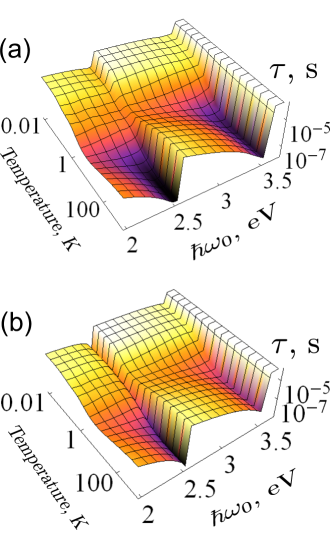
where and are exciton and surface plasmon dispersions, respectively, and is the matrix element of coupling. Here we have introduced the surface plasmon mode decay rate with two channels of decay: internal scattering in metal and scattering on the roughness of the metal surface. The latter can be followed by an emission of a photon, thus enhancing the light extraction from a sample. To emphasize plasmonic effects we neglect here the exciton damping. The temperature dependence of exciton decay through the plasmon mode can now be obtained by taking an imaginary part of the exciton-like branch of Eq. (3) and averaging it over the thermal distribution similarly to the Eq. (1). If the surface of metal is rough or consists of clusters, photons scattered at the interface may provide an additional channel for radiative decay of the SP1 mode. We will further present the results of calculations where both channels are taken into account. Fig. 4 shows the dependence of the exciton decay time through the plasmon modes on temperature and exciton resonance energy . The thicknesses of metal, barrier and quantum well layers are denoted as , and , respectively. Note that the frequency dependence of the decay time exhibits two dips at the positions of plasmonic resonances. As for the temperature behavior, it is strongly nonmonotonous and in the frequency region where both plasmon resonances are present ( eV for silver) it also exhibits two minima. Those minima become apparent if the thermal distribution function has its maximum in the region of anti-crossing between exciton and plasmon branches. Once the exciton resonant frequency moves to higher values one of the minima vanishes since only one plasmon mode is generated in this regime.
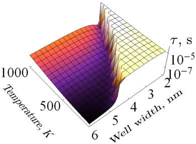
The exciton energy in a quantum well can be tuned to the plasmon resonance by variation of the well width and temperature. This tuning results in a significant decrease of the exciton lifetime, which is illustrated by Fig. 5. This figure offer a tool for life-time engineering in metal-semiconductor structures: tuning the thicknesses of well and barrier layers one can vary the exciton radiative lifetime by orders of magnitude.
In conclusion, we have shown that the coupling of excitons in quantum wells with the surface plasmons at metal-semiconductor and metal-air interfaces yileds additional channels of exciton radiative decay which may significantly reduce the exciton radiative lifetime. The temperature dependence of exciton radiative life-time becomes strongly non-monotonic in the presence of plasmons. It experiences two dips as the exciton gas heats up to the energies of two plasmon modes in an air-metal-semiconductor structure. The plasmon-controlled Purcell effect opens way to the life-time engineering in semiconductor-metal quantum confined structures which may be widely used in solid state light emitters.
References
- (1)
- (2)
- (3)
- (4)
- Koenderink (2010) A. F. Koenderink, Optics Letters 35, 4208 (2010).
- Meinzer et al. (2010) N. Meinzer, M. Ruther, S. Linden, C. M. Soukoulis, G. Khitrova, J. Hendrickson, J. D. Olitzky, H. M. Gibbs, and M. Wegener, Opt. Express 18 18, 24140 (2010).
- Anger et al. (2006) P. Anger, P. Bharadwaj, and L. Novotny, Phys. Rev. Lett. 96, 113002 (2006).
- Kühn et al. (2006) S. Kühn, U. Håkanson, L. Rogobete, and V. Sandoghdar, Phys. Rev. Lett. 97, 017402 (2006).
- Curto et al. (2010) A. G. Curto, G. Volpe, T. H. Taminiau, M. P. Kreuzer, R. Quidant, and N. F. van Hulst, Science 329, 930 (2010).
- Ajiki et al. (2002) H. Ajiki, T. Tsuji, K. Kawano, and K. Cho, Phys. Rev. B 66, 245322 (2002).
- Glazov et al. (2011) M. M. Glazov, E. L. Ivchenko, A. N. Poddubny, and G. Khitrova, Fiz. Tverd. Tela 53, 1665 (2011).
- Ford and Weber (1984) G. W. Ford and W. H. Weber, Phys. Rep. 113, 195 (1984).
- Chance et al. (1978) R. R. Chance, A. Prock, and R. Silbey, Adv. Chem. Phys. 37, 1 (1978).
- Gontijo et al. (1999) I. Gontijo, M. Boroditsky, E. Yablonovitch, S. Keller, U. K. Mishra, and S. P. DenBaars, Phys. Rev. B 60, 11564 (1999).
- Neogi et al. (2002) A. Neogi, C.-W. Lee, H. O. Everitt, T. Kuroda, A. Tackeuchi, and E. Yablonovitch, Phys. Rev. B 66, 153305 (2002).
- Okamoto et al. (2004) K. Okamoto, I. Niki, A. Shvartser, Y. Narukawa, T. Mukai, and A. Scherer, Nat. Mater. 3, 601 (2004).
- Okamoto et al. (2005) K. Okamoto, I. Niki, A. Scherer, Y. Narukawa, T. Mukai, and Y. Kawakami, Applied Physics Letters 87, 071102 (pages 3) (2005).
- Lin et al. (2010) J. Lin, A. Mohammadizia, A. Neogi, H. Morkoc, and M. Ohtsu, Applied Physics Letters 97, 221104 (pages 3) (2010).
- Jang et al. (2012) L.-W. Jang, D.-W. Jeon, T. Sahoo, D.-S. Jo, J.-W. Ju, S. jae Lee, J.-H. Baek, J.-K. Yang, J.-H. Song, A. Y. Polyakov, et al., Opt. Express 20, 2116 (2012).
- Toropov et al. (2009) A. A. Toropov, T. V. Shubina, V. N. Jmerik, S. V. Ivanov, Y. Ogawa, and F. Minami, Phys. Rev. Lett. 103, 037403 (2009).
- Tanaka et al. (2010) K. Tanaka, E. Plum, J. Y. Ou, T. Uchino, and N. I. Zheludev, Phys. Rev. Lett. 105, 227403 (2010).
- Ivchenko (2005) E. L. Ivchenko, Optical spectroscopy of semiconductor nanostructures (Alpha Science, Harrow UK, 2005).
- Pitarke et al. (2007) J. M. Pitarke, V. M. Silkin, E. V. Chulkov, and P. M. Echenique, Rep. Prog. Phys. 70, 1 (2007).
- Sanford et al. (2003) N. A. Sanford, L. H. Robins, A. V. Davydov, A. Shapiro, D. V. Tsvetkov, A. V. Dmitriev, S. Keller, U. K. Mishra, and S. P. DenBaars, Journal of Applied Physics 94, 2980 (2003).
- Ehrenreich and Philipp (1962) H. Ehrenreich and H. Philipp, Physical Review 128, 1622 (1962).
- Ehrenreich et al. (1963) H. Ehrenreich, H. Philipp, and B. Segall, Physical Review 132, 1918 (1963).
- Cooper et al. (1965) B. R. Cooper, H. Ehrenreich, and H. R. Philipp, Physical Review 138, A494 (1965).
- Maier (2007) S. Maier, Plasmoncs. Fundamentals and Applications (Springer, 2007).
- Bellessa et al. (2008) J. Bellessa, C. Symonds, C. Meynaud, J. C. Plenet, E. Cambril, A. Miard, L. Ferlazzo, and A. Lemaitre, Phys. Rev. B 78, 205326 (2008).