Optical properties of Bi2Te2Se at ambient and high pressure
Abstract
The temperature dependence of the complex optical properties of the three-dimensional topological insulator Bi2Te2Se is reported for light polarized in the a-b planes at ambient pressure, as well as the effects of pressure at room temperature. This material displays a semiconducting character with a bulk optical gap of meV at 295 K. In addition to the two expected infrared-active vibrations observed in the planes, there is additional fine structure that is attributed to either the removal of degeneracy or the activation of Raman modes due to disorder. A strong impurity band located at cm-1 is also observed. At and just above the optical gap, several interband absorptions are found to show a strong temperature and pressure dependence. As the temperature is lowered these features increase in strength and harden. The application of pressure leads to a very abrupt closing of the gap above 8 GPa, and strongly modifies the interband absorptions in the mid-infrared spectral range. While ab initio calculations fail to predict the collapse of the gap, they do successfully describe the size of the band gap at ambient pressure, and the magnitude and shape of the optical conductivity.
pacs:
72.20,-i, 74.62.Fj, 78.20.-eI Introduction
A topological insulator is a material in which a large spin-orbit interaction produces a band inversion over a bulk band gap, resulting in protected metallic surface states.Hsieh et al. (2008); Hasan and Kane (2010); Moore (2010) In the search for three dimensional topological insulators, the discovery of the layered bismuth chalcogenide Bi2Te3-xSex family was of particular importance.Zhang et al. (2009); Wang and Johnson (2011) The simple structure of the surface states in these compounds, with only one Dirac cone traversing the band gap,Hasan et al. (2009); Valla et al. (2012) has attracted a great deal of interest. The suitably-sized bulk band gap ( meV) and robust metallic surface states persisting up to high temperaturesValla et al. (2012) make this series of compounds interesting for experimental investigation, and potentially also in applications. However, difficulties concerning material purity and stoichiometry lead to a deteriorated insulating character of the bulk. Bismuth and tellurium have very similar electronegativity on Pauling’s scale,Gaudin et al. (1995) and this naturally leads to a large concentration of antisite defects. Bi2Te3 is not a line compound but exists in a narrow field of compositions (%);Abrikosov and Bankina (1958) as a result, a slight deficiency or excess of Te will result in either a p-type or n-type material, respectively.Satterthwaite and Ure (1957) Very often it is the case that Bi2Te3 crystals are p-type and have a high hole concentration because of a large number of negatively charged defects due to tellurium sites occupied by bismuth atoms.Kul’bachinskii et al. (2001) In Bi2Se3, on the other hand, because of the high fugacity of selenium, the concentration of selenium vacancies exceeds the concentration of antisite defects, so that the Bi2+xSe3 crystal typically exhibits n-type conductivity.Sklenár et al. (2000); Plecháček et al. (2002) All of these factors cause disorder (impurities) in the structure and lead to symmetry breaking and intrinsic doping. Contrary to the expected insulating state, a finite residual conductivity appears. The salient question is how to optimize these systems and decrease the bulk conductivity.
In an ordered stoichiometric structure Se vacancies can be decreased, and the Se/Te randomness diminished. Recently, it was found that Bi2Te2Se has the highest resistivity within the Bi2Te3-xSex family. Shubnikov–de Haas oscillations were observed and attributed to the surface states,Ren et al. (2010); Jia et al. (2011); Ren et al. (2012); Xiong et al. (2012) and a single Dirac cone crosses the Fermi surface.Ji et al. (2012) Angle-resolved photoemission spectroscopy (ARPES) shows narrow linewidths of topological surface states, which indicates that the disorder is suppressed.Neupane et al. (2012); Arakane et al. (2012)
To improve existing topological insulators and design new ones, it is necessary to understand the details of their band structure. It is important to know how the impurities influence the conductivity, and what happens if the lattice dimensions are varied, for example, through chemical substitutions. Much of this can be addressed through a careful study of the optical properties. The optical properties of Bi2Te3 and Bi2Se3 crystals have been intensely studied in the past century.Köhler and Becker (1974); *unkelbach73 More recently, this family of compounds has been revisited in light of the topological properties.LaForge et al. (2010); Di Pietro et al. (2012) In this paper we focus on Bi2Te2Se and investigate the temperature dependence of the complex optical properties in order to improve the understanding of the bulk response. Through room-temperature reflection and transmission experiments at ambient and high pressure, information is obtained about the nature of the band gap, residual conductivity, vibrational modes, and interband transitions. The application of pressure allows the band gap to be studied as the distance between the layers is decreased.
We observe a semiconducting response in the optical conductivity of Bi2Te2Se with a gap of cm-1 (0.3 eV); below the gap are two strong infrared-active phonons at and 118 cm-1, an impurity band centered at cm-1, as well as other weaker features. In addition, there is evidence of a low-energy impurity band at 30 – 40 cm-1, in agreement with a small transport gap extracted from the dc conductivity measurement. The low-energy interband absorptions display a pronounced temperature dependence. The application of pressure with a diamond-anvil cell in Bi2Te2Se reduces the inter-layer spacing, altering the band structure. The optical gap is at first unchanged, and then strongly reduced upon pressure increase. Reflectance studies reveal that the band structure is altered by the application of even a small amount of pressure. Ab initio calculations of the electronic structure and the optical conductivity confirm the sensitivity of interband absorptions to -axis compression. However, the calculations show that -axis compression has very little effect on the band gap.
II Experiment and calculation
Single crystals of Bi2Te2Se were grown by the floating zone method starting from the stoichiometric ratio of metallic bismuth and chalcogenide elements. Cleaving the crystal exposes lustrous mirror-like surfaces, which flake off very easily.
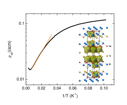
The structure of Bi2Te2Se is described by the trigonal space group (kawazulite) and shown in the inset of Fig. 1. The unit cell consists of quintuple Te–Bi–Se–Bi–Te layers stacked along the c-axis direction.Nakajima (1963); Bayliss (1991) The quintuple layers are bound by weak van der Waals interaction, which is responsible for the extreme ease with which the sample may be cleaved.
The temperature-dependent reflectance at ambient pressure was measured at a near-normal angle of incidence on a freshly-cleaved surface for light polarized in the a-b planes, from to over cm-1 (1.5 meV – 5.2 eV) using an in situ evaporation technique.Homes et al. (1993) The reflectance is a complex quantity, ; however, only the amplitude is measured in this experiment. To obtain the phase we employ the Kramers-Kronig relationDressel and Grüner (2001) using suitable extrapolations for the reflectance in the limits. At low frequencies the metallic Hagen-Rubens form for the reflectance is employed. Above the highest measured frequency point the reflectance is assumed to be constant up to cm-1, above which a free electron gas asymptotic reflectance extrapolation is assumed.Wooten (1972)
Raman spectra were collected using a home-made micro Raman spectrometer equipped with an argon laser at a wavelength of 514.5 nm, a half-meter monochromator and a liquid nitrogen-cooled CCD detector. The spectral resolution was of the order of 1 cm-1. The sample was mounted in a helium-flow cryostat allowing measurements down to 6 K with a long working distance objective.
Optical data at high pressure were recorded using a diamond anvil cell operated in transmission and reflection geometry. Type IIa diamonds with a culet of 0.55 mm were used with CuBe gaskets with a hole diameter of 250 m to apply pressures of up to 15 GPa inside a membrane-driven diamond anvil cell. Samples of Bi2Te2Se were cleaved to a thickness of a few microns. A fine dry KBr powder was used as the pressure-transmitting medium, and the pressure was monitored in situ through ruby fluorescence.Datchi et al. (2007) In the transmission geometry, light is focused on the sample in a home-made transmission setup with a pair of reflective objectives with a magnification coefficient of 15 and numerical aperture 0.5. For the reflectivity measurement, a Bruker Hyperion 3000 microscope was used with a single reflective objective. Infrared radiation was provided by the Swiss synchrotron light source (SLS) and coupledLerch et al. (2012) to the Fourier transform spectrometer. The high-brightness provided by the synchrotron source allows a spatial resolution of m2 or better while maintaining high throughput.
The band structure was calculated for the primitive cell containing 5 atoms. We used a full-potential linear muffin-tin-orbital (LMTO) programSavrasov (1996) within a local spin-density approximation (LSDA) and generalized gradient approximation (GGA).Perdew et al. (1996) The effect of spin-orbit coupling was taken into account.Larson et al. (2002); Dai et al. (2012) The -mesh was for the self consistency calculation, and for the calculation of the optical conductivity. The energy cutoff was set at 730 eV, and the convergence criterium is such that total energy accuracy is better than eV.
III Results and discussion
The resistivity measured in the a-b plane is shown in Fig. 1 in an Arrhenius plot (log against ). At 5 K, . From room temperature down to K the behavior of the resistivity is similar to that of a bad metal. The value of at room temperature is m, and the temperature slope is small and positive, cm/K. Between 170 and 30 K we see activated behavior with the transport gap meV; a fit to the activated behavior is shown in Fig. 1. At the lowest temperatures the gap appears to decrease down to meV, pointing to a contribution from activation of donor (acceptor) levels, and the metallic surface states. In comparison with previously reported results,Ren et al. (2010); Jia et al. (2011) our sample has a smaller activation energy; previous reports are in the range meV. The residual resistivity at low temperatures is times smaller than in the previous reports.Ren et al. (2010); Jia et al. (2011) However, the transport gaps observed in other works in the K limit are much smaller, eV, hinting at a more significant contribution from activation of donor/acceptor levels and the surface states than in our sample. The difference in transport properties is probably related to minute stoichiometry differences. The measurement of thermopower on a sample from the same batch showed that the charge carriers in the sample are electrons.Akrap et al. (2012)
III.1 Energy gap
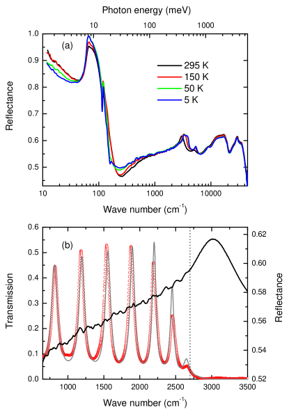
The temperature dependence of the reflectance of Bi2Te2Se for the light polarized in the a-b plane is shown over a wide frequency range in Fig. 2(a); the region close to the band edge is shown in more detail in Fig. 2(b) at 295 K. The reflectance in the far infrared displays a weakly metallic character and is dominated by a strong low-frequency phonon mode. A weaker phonon mode can be distinguished above 100 cm-1 as a small notch superimposed on the stronger feature. At higher energies structures due to the gap edge at meV and several interband transitions are clearly visible in the reflectance. In addition, some of these features have a pronounced temperature dependence.
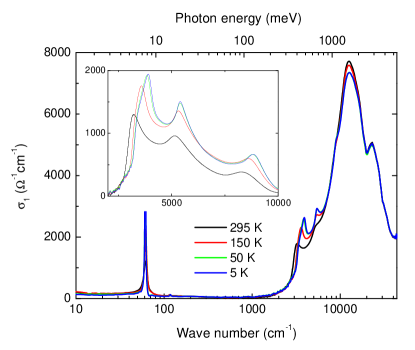
The real part of the optical conductivity () has been determined from a Kramers-Kronig analysis of the reflectance and is shown over a wide range in Fig. 3. The most prominent features are the strongly temperature-dependent interband absorptions associated with the band edge and a very strong low-energy vibration at cm-1. From the optical band gap can be roughly estimated to cm-1 (300 meV) at 295 K. The onset of the gap in Bi2Te2Se is much sharper than in Bi2Se3,LaForge et al. (2010) where the natural Se deficiency results in intrinsic doping and a well-defined metallic (Drude-like) contribution. It may be noted that the transport gap extracted from the resistivity measurement is almost two orders of magnitude smaller than the optical band gap, which suggests that conduction occurs as a result of hopping through localized impurity states within the gap.
An improved estimate of the band gap may be obtained from combining the reflectance and transmission measurements. A comparison of the reflectance of the bulk material and the transmission through a thin sample at 295 K is shown in Fig. 2(b). Strong Fabry-Perot oscillations are observed in the transmission in the mid-infrared region; however, weak fringes are also observed in the reflectance. The explanation for this is that the sample cleaves extremely easily and its surface inevitably terminates in thin flakes. A part of the incident light is reflected while another part is transmitted through the flake and reflected from the back surface; the back reflection interferes with the primary reflection and produces fringes. A dashed vertical line at 2700 cm-1 (335 meV) indicates where the Fabry-Perot oscillations in both the reflectance and transmission appear to terminate. The transmission data has been fit using a Tauc-Lorentz modelJellison and Modine (1996a); *jellison96b for the dielectric function in which a modified Lorentzian oscillator [see Eq. (2)] is used to describe the interband absorptions; the imaginary part is written as
| (1) |
The fitted parameters , , and correspond to the intensity, broadening, transition energy, and energy gap, respectively. The real part is determined from a Kramers-Kronig analysis of , allowing the transmission to be calculated for a thin slab.ref Pieces of varying thickness ( – 9 m) have been examined, and the fit to the transmission through a 2 m thick flake of Bi2Te2Se is shown in Fig. 2(b). The band gap was determined in samples with several different thicknesses to be meV [ cm-1], which is somewhat lower than the energy at which the fringes are observed to disappear.
The optical properties of the bulk are described using the Drude-Lorentz model for the complex dielectric function
| (2) |
where is the real part of the dielectric function at high frequency, and are the square of the plasma frequency and scattering rate for the delocalized (Drude) carriers, respectively, and is an effective mass. For the Lorentz oscillators , and represent the position, width, and strength of the th vibration or excitation. The complex conductivity is .
In addition to the vibrational parameters, discussed in Sec. III B, a fit to the low-frequency conductivity at room temperature yields cm-1 and cm-1; this value for the plasma frequency corresponds to a carrier concentration of cm-3, consistent with previous results.Satterthwaite and Ure (1957)
One of the more interesting aspects of this material is the unusual temperature dependence of the interband transition associated with the gap edge, shown in Fig. 3, in which the increase in intensity, or spectral weight (defined as the area under the conductivity curve over a given frequency interval) of this feature, or set of features, in the cm-1 region, is compensated for by a loss of spectral weight at high frequency. This behavior may be shown in more detail by fitting the strong high-frequency features at and cm-1 and then subtracting this contribution from the conductivity. The result of this procedure is shown in the inset of Fig. 3. At low temperature the peak of the lowest interband absorption hardens by cm-1 and develops a weak shoulder, while the two higher-energy features appear symmetric and display smaller blue shifts. The gap edge appears to harden by cm-1.
The thermal shifts in the gap edge and the absorption peaks are significant. One effect of the decrease in temperature is that the lattice contracts, which leads to an increase in the band gap.Lautenschlager et al. (1985) However, a more important process is the phonon absorption and re-emission. The highest-energy phonons in the system (Sec. III B) set a temperature scale of approximately 170 K. When the temperature is much lower than this, the phonon processes become inaccessible and the gap increases. While the strong temperature dependence of the gap may be understood with phonons, the unusual shifts of the interband absorptions are more likely linked to the contraction of the lattice.
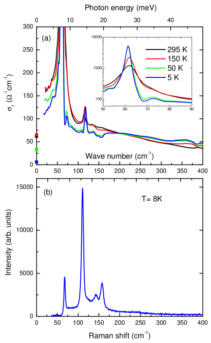
At long wavelengths the optical conductivity is consistent with the dc transport: the conductivity is very small and it further decreases as temperature is lowered. As shown in Fig. 4(a), the values of extrapolate roughly to the values of the dc conductivity. Since the dc conductivity at low temperatures is finite, there is also a weak free-carrier (Drude-like) contribution. However, it is impossible to accurately model this since it is masked by larger effects; a strong background which peaks around the 62 cm-1 phonon and persists up to at least 400 cm-1. A part of this broad background may be identified as a far-infrared band due to the presence of impurities. The impurity band is slightly enhanced as the temperature is lowered. This is in agreement to what was previously reported in Bi2Te2Se and attributed to impurities.Di Pietro et al. (2012) A similar impurity band was also observed several years ago in a series of doped semiconductors, Si:P.Gaymann et al. (1995) The presence of impurity states in the low-energy excitations agrees with the small transport gap obtained from the resistivity measurement. A wide impurity band is centered at cm-1, but there may be another impurity band centered at cm-1 ( meV), lying in the side band of the strong optical phonon. While the latter impurity band would agree with the small activation energy obtained in the resistivity measurement, it is possible that this feature is instead linked to the strong low-lying phonon, discussed in the following Section.
III.2 Vibrational properties
The optical conductivity of Bi2Te2Se allows the vibrational properties to be analyzed. As Fig. 4(a) shows, only two sharp phonon peaks are observed at room temperature. At low temperatures these vibrations further sharpen, but in addition several other, albeit much weaker, modes appear. The symmetry group analysis of Bi2Te2Se in the setting gives the irreducible vibrational representationKöhler and Becker (1974); Richter and Becker (1977)
| (3) |
Here, the and modes are Raman-active. The and modes are infrared active along the c axis and the a-b planes, respectively. The two modes can be identified as the two strong vibrations observed at 62 cm-1 and 117 cm-1.Cheng and Ren (2011) As the temperature is decreased, the low-energy mode softens, while the higher-energy mode hardens. At low temperatures the 62 cm-1 mode, shown in the inset of Fig. 4(a), appears to develop a slight asymmetry, with a tail at low frequencies. An inhomogeneous structure would be enough to cause an asymmetry in such a strong phonon mode; however, small level shifts in the reflectance can also artificially produce an asymmetry in the line shape of a strong phonon in an insulator.
| Infrareda | |||
|---|---|---|---|
| mode | |||
| 51.6 (0.1) | 8.3 (0.7) | 133 (11) | |
| 61.7 (0.03) | 2.0 (0.1) | 936 (25) | |
| 72.7 (0.04) | 7.0 (0.3) | 114 (4) | |
| 108.0 (0.1) | 6.1 (0.7) | 40 (4) | |
| 117.8 (0.02) | 6.0 (0.1) | 159 (2) | |
| 137.1 (0.08) | 8.5 (0.5) | 55 (2) | |
| 149.0 (0.09) | 5.0 (0.5) | 22 (2) | |
| (Antiresonanceb) | |||
| 144.1 (0.1) | 9.0 (0.5) | 68 (3) | |
| 155.8 (0.1) | 13.1 (0.8) | 100 (4) | |
| Raman | |||
| mode | |||
| 67.7 (0.1) | 3.5 (0.2) | 0.21 | |
| 110.7 (0.1) | 5.1 (0.1) | 1.00 | |
| 142.2 (0.5) | 19.6 (3.5) | 0.35 | |
| 157.7 (0.2) | 7.1 (0.4) | 0.27 | |
The infrared-active modes observed at 5 K have been fit to Lorentz oscillators with a polynomial background and the frequencies, widths and strengths are listed in Table 1. Contrary to previous experiments on Bi2Se3,LaForge et al. (2010) we can find no convincing evidence of Fano-like behavior in the strong phonon at cm-1. In addition to the two allowed in-plane infrared modes, there are at least seven other infrared-active modes observed. It is possible that disorder may lead to the lifting of the degeneracy of the modes, leading to weak splitting. However, we note that the fit to the conductivity by employing two resonances at and 149 cm-1 may actually be improved by considering two Fano antiresonancesHomes et al. (1995) at and 155.8 cm-1, respectively. The Raman spectrum is shown at 8 K in Fig. 4(b). The energies of the Raman-active modes are very close to the energies of some of the weak phonons that appear in the conductivity at low temperature; it is possible that symmetry breaking may lead to the activation of Raman modes that are normally not infrared active. In particular the positions of the two antiresonances in the conductivity are very close to the two high-frequency Raman modes at 142 and 158 cm-1 (Table 1). In low-dimensional materials, the totally-symmetric Raman modes have been observed to undergo out-of-phase coupling to produce an optically-active mode at the same frequency as the Raman mode;Rice (1976) in systems where these modes sit upon a strong electronic background they appear as antiresonances rather than resonances.Jacobsen et al. (1983) A similar mechanism may be responsible for the Fano-like line shapes observed in this material. Since we seem to observe at least nine modes in total, it is also possible that the out-of-plane modes may also be activated by disorder or a slight misalignment; these vibrations typically manifest themselves in the planes at the longitudinal-optic positions.Reedyk and Timusk (1992) Overall, the low-energy optical and vibrational properties of Bi2Te2Se point towards the importance of substitutional disorder and intrinsic doping.
III.3 Pressure
The structure of Bi2Te2Se appears to be “soft” or easily compressible along the c-axis, where the quintuple atomic layers are linked by weak van der Waals interaction (inset of Fig. 1). A natural question is how sensitive this material is to pressure. Indeed, the changes in the gap under pressure in the related compounds Bi2Te3 and Bi2Se3 suggest that hydrostatic pressure is very effective at tuning the band structure. In Bi2Te3, Vilaplana et al.Vilaplana et al. (2011a); *vilaplana11b report reducing the gap from 170 to 120 meV by applying 6 GPa. In Bi2Se3 the optical gap is increased from 170 meV at ambient pressure to 450 meV at 8 GPa.Segura, A. and Panchal, V. and Sánchez-Royo, J. F. and Marín-Borrás, V. and Muñoz-Sanjosé, V. and Rodríguez-Hernández, P. and Muñoz, A. and Pérez-González, E. and Manjón, F. J. and González, J. (2012)
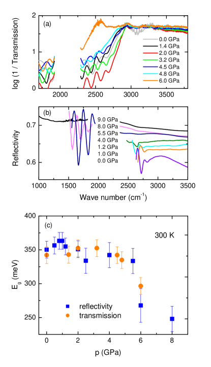
In Fig. 5(a), is plotted as a function of frequency for different pressures at room temperature. Transmission through a thin film of thickness is given byvan Heumen and van der Marel (2006)
| (4) |
so that represents an approximation to the real part of the conductivity, offset by a constant. The gap may be simply estimated as the energy at half of the maximum value of . The oscillations below the gap edge are caused by the Fabry-Perot interference, previously illustrated in Fig. 2(b). The pressure dependence of the gap may also be obtained from the reflectivity measurements, shown in Fig. 5(b). Below the gap edge, strong Fabry-Perot oscillations appear and the energy of their onset may be taken as the value of the gap. Fig. 5(c) shows the pressure dependence of the gap determined from the transmission and reflectivity measurements as described above; the two estimates agree very well.
Up to 4 GPa, the effect of pressure on the gap edge in Bi2Te2Se is fairly modest, especially when compared to Bi2Te3 or Bi2Se3.Vilaplana et al. (2011a); Segura, A. and Panchal, V. and Sánchez-Royo, J. F. and Marín-Borrás, V. and Muñoz-Sanjosé, V. and Rodríguez-Hernández, P. and Muñoz, A. and Pérez-González, E. and Manjón, F. J. and González, J. (2012) However, a steep decrease in the gap value begins above 4 GPa, and by 8 GPa the gap has moved from to meV.
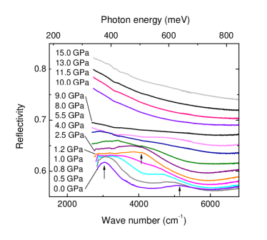
A wider spectral range for the reflectivity measured under pressure is shown in Fig. 6. For clarity, only the data above cm-1 is shown. Already below 1 GPa, the reflectivity changes significantly as pressure is applied. At the lowest pressures, up to 0.8 GPa, the two lowest interband transitions at and 5000 cm-1 are still distinguishable. As the pressure increases to 1.0 GPa, these two peaks merge into a single peak at cm-1. When the pressure is further increased, the reflectivity level increases. Above – 10 GPa the gap can no longer be followed. Extrapolating the data in Fig. 5 the system is expected to become metallic above 10 GPa.
In order to compare our data with the band structure predictions, the inset of Fig. 7 shows a comparison between the experimentally determined at 5 K and the calculated for an uncompressed lattice. Overall, the agreement is quite good and the value of the gap is approximately correct. The absorption bands are all reproduced, despite a minor shift in frequency.
The main panel of Fig. 7 shows the calculated conductivity for different lattice compressions. The effect of pressure on this layered structure was simulated as a reduction of inter-planar distances along the c axis while keeping the a-b plane lattice parameters constant. In this way we only change the distance between quintuple layers, linked by van der Waals interactions. All the other bonds are covalent and therefore much less compressible. The calculated gap edge does not significantly depend on -axis compression. On the contrary, the absorptions above the gap edge, marked by arrows in Fig. 7, show pressure dependence. For 5% compression of the c axis, only one peak remains below cm-1. This agrees with the reflectivity under pressure, which shows that the two structures below 6000 cm-1 merge into one for pressures above 1.0 GPa.
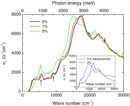
Overall, the high-pressure behavior of optical properties in Bi2Te2Se suggests that its band structure is very sensitive to pressure. The collapse of the gap does not seem to be captured by the LDA calculations in which only -axis compression is considered. This indicates that the changes of the geometry within a quintuple layer may play an important role in the closing of the gap under pressure.
IV Conclusions
The optical properties of Bi2Te2Se have been determined over a wide temperature and frequency range. The far-infrared optical conductivity indicates the presence of an impurity band at cm-1 (25 meV), well below the band gap. Numerous in-plane vibrational modes can be identified at 5 K in Bi2Te2Se, at least seven more than what is allowed by symmetry. Both the extra phonon modes and the impurity band are consistent with presence (and importance) of disorder and symmetry breaking in this material.
The band gap edge is determined to be meV at room temperature. At low temperatures shifts strongly to higher energies. Similarly, several interband transitions or absorptions above the gap edge show strong temperature dependence. Their behavior indicates that the band structure is significantly influenced by thermal contraction of the lattice.
The high-pressure optical properties of Bi2Te2Se have been determined at room temperature. A strong suppression of the gap edge occurs above 4.5 GPa. Commencing at low pressures, GPa, absorptions above the gap edge show a strong pressure dependence. Our measurements are in reasonable agreement with LSDA calculations.
Acknowledgements.
We would like to thank Philip Allen and Alexey Kuzmenko for helpful discussions. Thanks are due to Alfredo Segura for very useful technical advice. Research was supported by the Swiss NSF through grant No. 200020-135085 and its NCCR MaNEP. Work at BNL was supported by the U.S. Department of Energy, Office of Basic Energy Sciences, Division of Materials Sciences and Engineering under Contract No. DE-AC02-98CH10886. A.A. acknowledges funding from “Boursières d’Excellence” of the University of Geneva.References
- Hsieh et al. (2008) D. Hsieh, D. Qian, L. Wray, Y. Xia, Y. S. Hor, R. J. Cava, and M. Z. Hasan, Nature (London) 452, 970 (2008).
- Hasan and Kane (2010) M. Z. Hasan and C. L. Kane, Rev. Mod. Phys. 82, 3045 (2010).
- Moore (2010) J. E. Moore, Nature 464, 194 (2010).
- Zhang et al. (2009) H. Zhang, C.-X. Liu, X.-L. Qi, X. Dai, Z. Fang, and S.-C. Zhang, Nature Phys. 5, 438 (2009).
- Wang and Johnson (2011) L.-L. Wang and D. D. Johnson, Phys. Rev. B 83, 241309 (2011).
- Hasan et al. (2009) M. Hasan, H. Lin, and A. Bansil, Physics 2, 108 (2009).
- Valla et al. (2012) T. Valla, Z.-H. Pan, D. Gardner, Y. S. Lee, and S. Chu, Phys. Rev. Lett. 108, 117601 (2012).
- Gaudin et al. (1995) E. Gaudin, S. Jobic, M. Evain, and R. Brec, Materials Research Bulletin 30, 549 (1995).
- Abrikosov and Bankina (1958) N. Abrikosov and V. Bankina, Zhurnal Neorganicheskoi Khimii 3, 659 (1958).
- Satterthwaite and Ure (1957) C. B. Satterthwaite and R. W. Ure, Phys. Rev. 108, 1164 (1957).
- Kul’bachinskii et al. (2001) V. Kul’bachinskii, A. Kaminskii, K. Kindo, Y. Narumi, K. Suga, P. Lostak, and P. Svanda, JETP Letters 73, 352 (2001).
- Sklenár et al. (2000) A. Sklenár, C. Drasar, A. Krejcová, and P. Losták, Crystal Research and Technology 35, 1069 (2000).
- Plecháček et al. (2002) T. Plecháček, J. Navrátil, and J. Horák, Journal of Solid State Chemistry 165, 35 (2002).
- Ren et al. (2010) Z. Ren, A. A. Taskin, S. Sasaki, K. Segawa, and Y. Ando, Phys. Rev. B 82, 241306(R) (2010).
- Jia et al. (2011) S. Jia, H. Ji, E. Climent-Pascual, M. K. Fuccillo, M. E. Charles, J. Xiong, N. P. Ong, and R. J. Cava, Phys. Rev. B 84, 235206 (2011).
- Ren et al. (2012) Z. Ren, A. A. Taskin, S. Sasaki, K. Segawa, and Y. Ando, Phys. Rev. B 85, 155301 (2012).
- Xiong et al. (2012) J. Xiong, A. Petersen, D. Qu, Y. Hor, R. Cava, and N. Ong, Physica E 44, 917 (2012).
- Ji et al. (2012) H. Ji, J. M. Allred, M. K. Fuccillo, M. E. Charles, M. Neupane, L. A. Wray, M. Z. Hasan, and R. J. Cava, Phys. Rev. B 85, 201103(R) (2012).
- Neupane et al. (2012) M. Neupane, S.-Y. Xu, L. A. Wray, A. Petersen, R. Shankar, N. Alidoust, C. Liu, A. Fedorov, H. Ji, J. M. Allred, Y. S. Hor, T.-R. Chang, H.-T. Jeng, H. Lin, A. Bansil, R. J. Cava, and M. Z. Hasan, Phys. Rev. B 85, 235406 (2012).
- Arakane et al. (2012) T. Arakane, T. Sato, S. Souma, K. Kosaka, K. Nakayama, M. Komatsu, T. Takahashi, Z. Ren, K. Segawa, and Y. Ando, Nature Commun. 3, 636 (2012).
- Köhler and Becker (1974) H. Köhler and C. R. Becker, phys. stat. sol. (b) 61, 533 (1974).
- Unkelbach et al. (1973) K. Unkelbach, C. Becker, H. Köhler, and A. Middendorff, Physica Status Solidi (b) 60, K41 (1973).
- LaForge et al. (2010) A. D. LaForge, A. Frenzel, B. C. Pursley, T. Lin, X. Liu, J. Shi, and D. N. Basov, Phys. Rev. B 81, 125120 (2010).
- Di Pietro et al. (2012) P. Di Pietro, F. M. Vitucci, D. Nicoletti, L. Baldassarre, P. Calvani, R. Cava, Y. S. Hor, U. Schade, and S. Lupi, Phys. Rev. B 86, 045439 (2012).
- Nakajima (1963) S. Nakajima, Journal of Physics and Chemistry of Solids 24, 479 (1963).
- Bayliss (1991) P. Bayliss, Amer. Mineral. 76, 257 (1991).
- Homes et al. (1993) C. C. Homes, M. Reedyk, D. A. Crandles, and T. Timusk, Appl. Opt. 32, 2976 (1993).
- Dressel and Grüner (2001) M. Dressel and G. Grüner, Electrodynamics of Solids (Cambridge University Press, Cambridge, 2001).
- Wooten (1972) F. Wooten, Optical Properties of Solids (Academic Press, New York, 1972) pp. 244–250.
- Datchi et al. (2007) F. Datchi, A. Dewaele, P. Loubeyre, R. Letoullec, Y. Le Godec, and B. Canny, High Pressure Research 27, 447 (2007).
- Lerch et al. (2012) P. Lerch, L. Quaroni, J. Wambach, J. Schneider, D. Armstrong, D. Rossetti, F. Mueller, P. Peier, V. Schlott, L. Carroll, P. Friedli, H. Sigg, S. Stutz, and M. Tran, Journal of Physics: Conference Series 359, 012003 (2012).
- Savrasov (1996) S. Y. Savrasov, Phys. Rev. B 54, 16470 (1996).
- Perdew et al. (1996) J. P. Perdew, K. Burke, and M. Ernzerhof, Phys. Rev. Lett. 77, 3865 (1996).
- Larson et al. (2002) P. Larson, V. A. Greanya, W. C. Tonjes, R. Liu, S. D. Mahanti, and C. G. Olson, Phys. Rev. B 65, 085108 (2002).
- Dai et al. (2012) X.-Q. Dai, B. Zhao, J.-H. Zhao, Y.-H. Li, Y.-N. Tang, and N. Li, Journal of Physics: Condensed Matter 24, 035502 (2012).
- Akrap et al. (2012) A. Akrap, A. Ubaldini, E. Giannini, and L. Forró, arXiv:1210.3901v1 (2012).
- Jellison and Modine (1996a) G. E. Jellison and F. A. Modine, Appl. Phys. Lett. 69, 371 (1996a).
- Jellison and Modine (1996b) G. E. Jellison and F. A. Modine, Appl. Phys. Lett. 69, 2137 (1996b).
- (39) A. Kuzmenko, computer code, RefFIT (University of Geneva, Geneva, Switzerland).
- Lautenschlager et al. (1985) P. Lautenschlager, P. B. Allen, and M. Cardona, Phys. Rev. B 31, 2163 (1985).
- Gaymann et al. (1995) A. Gaymann, H. P. Geserich, and H. v. Löhneysen, Phys. Rev. B 52, 16486 (1995).
- Richter and Becker (1977) W. Richter and C. R. Becker, phys. stat. sol. (b) 84, 619 (1977).
- Cheng and Ren (2011) W. Cheng and S.-F. Ren, Phys. Rev. B 83, 094301 (2011).
- Homes et al. (1995) C. C. Homes, T. Timusk, D. A. Bonn, R. Liang, and W. N. Hardy, Can. J. Phys. 73, 663 (1995).
- Rice (1976) M. J. Rice, Phys. Rev. Lett. 37, 36 (1976).
- Jacobsen et al. (1983) C. S. Jacobsen, D. B. Tanner, and K. Bechgaard, Phys. Rev. B 28, 7019 (1983).
- Reedyk and Timusk (1992) M. Reedyk and T. Timusk, Phys. Rev. Lett. 69, 2705 (1992).
- Vilaplana et al. (2011a) R. Vilaplana, O. Gomis, F. J. Manjón, A. Segura, E. Pérez-González, P. Rodríguez-Hernández, A. Muñoz, J. González, V. Marín-Borrás, V. Muñoz Sanjosé, C. Drasar, and V. Kucek, Phys. Rev. B 84, 104112 (2011a).
- Vilaplana et al. (2011b) R. Vilaplana, D. Santamaría-Pérez, O. Gomis, F. J. Manjón, J. González, A. Segura, A. Muñoz, P. Rodríguez-Hernández, E. Pérez-González, V. Marín-Borrás, V. Muñoz Sanjose, C. Drasar, and V. Kucek, Phys. Rev. B 84, 184110 (2011b).
- Segura, A. and Panchal, V. and Sánchez-Royo, J. F. and Marín-Borrás, V. and Muñoz-Sanjosé, V. and Rodríguez-Hernández, P. and Muñoz, A. and Pérez-González, E. and Manjón, F. J. and González, J. (2012) Segura, A. and Panchal, V. and Sánchez-Royo, J. F. and Marín-Borrás, V. and Muñoz-Sanjosé, V. and Rodríguez-Hernández, P. and Muñoz, A. and Pérez-González, E. and Manjón, F. J. and González, J., Phys. Rev. B 85, 195139 (2012).
- van Heumen and van der Marel (2006) E. van Heumen and D. van der Marel, in Lectures on the Physics of Strongly Correlated Systems XI: Eleventh Training Course in the Physics of Strongly Correlated Systems, edited by F. Mancini and A. Avella (AIP Conference Proceedings 918, 2006).