Electronic and optical properties of potential solar absorber Cu3PSe4
Abstract
We theoretically investigate the electronic and optical properties of semiconductor Cu3PSe4. We also report diffuse reflectance spectroscopy measurements for Cu3PSe4 and Cu3PS4, which indicate a band gap of 1.40 eV for the former. Hybrid functional calculations agree well with this value, and reveal that the band gap is direct. Calculations yield an optical absorption spectrum similar to GaAs in the visible region, with cm-1 for nm. We conclude that the optical properties of Cu3PSe4 are within the desired range for a photovoltaic solar absorber material.
pacs:
71.20.Nr, 78.40.Fy, 78.20.BhThe need for low cost solar photovoltaic cells continues to drive a global effort to find, evaluate, and refine materials that offer both cost effective and highly efficient solutions. Within the search among the inorganic semiconductors, one of the most exciting families has been the ternary and quaternary copper chalcogenides consisting of CuCh4 and ACh4 tetrahedra, where Ch is one of (S, Se, Te) and A represents one or more other elements. Examples include the commercially widespread Cu(In,Ga)Se2 (CIGS), as well as Cu2ZnSnS4, which has the benefit of consisting of low-toxicity, readily available elements. One material in this family which has not received much attention in this regard is Cu3PSe4. The structure of Cu3PSe4 has been determinedGarin and Parthé (1972); Ma et al. (2002), and a photoelectrochemical analysisMarzik et al. (1983) of isostructural compounds Cu3PS4 and Cu3PS3Se has indicated indirect bandgaps of 2.38 eV and 2.06 eV respectively. However the bandgap of Cu3PSe4 itself has not been reported previously. In this Letter we examine this material, theoretically in the scope of low temperature and zero defects, and experimentally in the scope of room temperature measurements on powder samples.
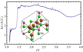
In our synthesis of Cu3PSe4 and Cu3PS4, elemental powders of Cu (Cerac, 99.5%), P (Alpha Aesar 99%), Se (Cerac, 99.6%), and S (Cerac, 99.999%), are ground and sealed in evacuated fused silica tubes. Polycrystalline powders are obtained via solid state reaction at 480 ∘C (Cu3PSe4) and 600 ∘C (Cu3PS4) for 24 h. The XRD patterns, collected on a Rigaku Ultima IV, of the reacted samples are similar to the ISCD card 095412 for Cu3PSe4 and 412240 for Cu3PS4. Hole majority carrier type is confirmed by positive thermoelectric voltage measurements. The optical bandgaps are determined from diffuse reflectance measurements (see Figure 1) collected with a spectrometer equipped with an Ocean Optics HR4000 UV-VIS detector and a balanced deuterium/tungsten halogen source (DH-2000-BAL). The Kubelka-Munk model is employed to determine the optical absorption edges of 1.40 eV and 2.38 eV for Cu3PSe4 and Cu3PS4, respectively. The Cu3PSe4 bandgap is within the desired range for solar photovoltaic devices (1.0 eV to 1.6 eV), while the Cu3PS4 bandgap agrees precisely with Ref. [Marzik et al., 1983].
Calculations based on density functional theory (DFT) are performed using the projector augmented wave (PAW) methodBloechl (1994); *kresse_ultrasoft_1999 as implemented in the plane wave code VASPKresse and Furthmüller (1996). For the exchange-correlation functional we use the generalized gradient approximation (GGA) in the PW91 parametrizationPerdew et al. (1992) for accurate total energy calculations. To avoid the bandgap underestimation common to standard DFT calculationsStampfl and de Walle (1999), we use the Heyd-Scuseria-ErnzerhofHeyd, Scuseria, and Ernzerhof (2003); *heyd_erratum:_2006 (HSE) hybrid functional, which combines Hartree-Fock (HF) exchange with GGA exchange and includes an empirical shielding of the HF exchange. The HSE functional has yielded respectable estimates for semiconductor bandgapsPeralta et al. (2006); *kim_accurate_2009; *chan_efficient_2010, although it is generally not as reliable as methods based on the approximation.Shishkin and Kresse (2007) We will see below that HSE performs particularly well for calculations on Cu3PSe4. For brevity and the expressed application interest, we present theoretical analysis for Cu3PSe4 but not Cu3PS4. Both materials crystallize in the wurtzite-based enargite structure with a simple orthorhombic unit cell with 16 atoms admitting the space group (FIG. 1).
For electronic and optical calculations, we use experimentally determined lattice and atomic parameters.Ma et al. (2002) Ionic and lattice relaxations are discussed below. In all calculations, we carefully consider the convergence of the result with respect to plane wave basis cut-off energy, -point density, and time saving approximations.
The HSE determined band structure is shown in FIG. 2.
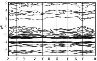
The HSE calculations used a -centered -point grid with down-sampling for one of the -point summations in the evaluation of the Hartree-Fock exchange potential.Paier et al. (2006) The band structure plot itself (FIG. 2) is formed by interpolation of the -point grid using a Fourier method.Pickett, Krakauer, and Allen (1988) The band structure most importantly shows a direct bandgap of 1.38 eV at the point, in excellent agreement with the experimental value of eV. The band structure also shows low lying valleys ( eV) in both the valence band (at Y) and the conduction band (along -Z). We note that an HSE calculation for Cu3PS4 at experimental parametersPfitzner and Reiser (2002) gives these two valleys as being the valence band maximum (VBM) and conduction band minimum (CBM), with theoretical and experimentalMarzik et al. (1983) indirect bandgaps of 2.55 eV and 2.38 eV respectively. We calculate electron and hole effective masses of 0.17 and 0.60 times the electron mass, respectively. Spin-orbit coupling was verified to be small in a single GGA calculation which showed VBM splitting and a bandgap decrease of 0.030 eV relative to the spinless GGA bandgap of 0.29 eV.
An analysis of the partial density of states indicates that the valence bands from the VBM to about eV below (see FIG. 2) have similar orbital composition to the corresponding bands of Cu2ZnSnS4.Paier et al. (2009) In particular, the valence band edge has anti-bonding Cu-d/Se-p∗ hybrid character, with the corresponding bonding states lying in the second valence band. Between these regions, at the bottom of the first valence band, lies the very dense bundle of non-bonding Cu-d orbitals. The two states in the lowest conduction band show hybridization among Se-p, P-s, and Cu-d orbitals. The charge density distributions of these states indicate significant anti-bonding character between P and Se ions. This will have important effects on relaxation calculations, as discussed below.
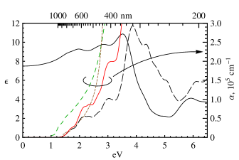
To obtain the optical properties of Cu3PSe4, the complex dielectric tensor has been calculatedGajdos et al. (2006) in the random phase approximation from HSE wavefunctions without including local effects, which are generally small.footnote1 The direction-averaged dielectric function and optical absorption coefficient are shown in Figure 3. Optical absorption is compared with experimental dataPalik (1991); Paulson, Birkmire, and Shafarman (2003) for GaAs and polycrystalline CuIn1-xGaxSe2 for . (In photovoltaic applications, CIGS stoichiometries near yield the most efficient power conversion.Kemell, Ritala, and Leskelä (2005)) For nm, the absorption in Cu3PSe4 is calculated to be higher than in GaAs. The greater absorption of CIGS is primarily due to its absorption curve being shifted to lower energies by its smaller bandgap (1.17 eV). While allowing absorption of a greater fraction of the solar spectrum, the CIGS bandgap limits its solar cell voltage—and its maximum theoretical efficiency—relative to larger bandgap materials. Absorption is above cm-1 for wavelengths nm ( eV)[ThisdatapointisapproximatelysharedwithCu$_2$ZnSnS$_4$whichhassimilarabsorption.]ito88ele and above cm-1 for nm ( eV).
As discussed previously, the HSE bandgap using the experimental atomic and lattice parameters agrees well with the measured bandgap. However, using GGA or local density approximation (LDA) relaxed structural parameters, we calculate HSE bandgaps approximately 30% smaller (TAB. 1). While the bandgap is expected to depend on the lattice parameters, such a large change is unusual, but can readily be understood as follows: An HSE ion relaxation leaves the experimental structure and bandgap nearly unchanged. The LDA and GGA relaxations, however, result in a lengthening of the P-Se bond, accompanied by large reductions of the HSE bandgap. The observed relation between the increase of the P-Se bond length and the underestimate of the calculated bandgaps is a direct consequence of the significant P-s/Se-p∗ anti-bonding character of the states at the conduction band edge: an underestimate of the bandgap (as in LDA/GGA) moves the P-s/Se-p∗ anti-bonding orbitals to lower energies, resulting in a smaller P-Se bond energy and a correspondingly longer bond. A similar bond length dependence of the bandgap of CuInSe2 is discussed in Ref. [Jaffe and Zunger, 1984].
| relaxation | (HSE) | () | P-Se | Cu-Se | |
|---|---|---|---|---|---|
| (eV) | (eV) | (Å3) | (Å) | (Å) | |
| LDA ion | 0.94 | 0.08111An indirect bandgap is predicted (0.04 eV, VBM along -Y in both cases). | 326.19 | 2.30 | 2.39 |
| LDA full | 1.10222An indirect bandgap is predicted (1.04 eV, CBM along -Z). | 0.06 | 310.59 | 2.27 | 2.35 |
| GGA ion | 1.02 | 0.03 | 326.19 | 2.29 | 2.40 |
| GGA full | 0.90 | 0.08111An indirect bandgap is predicted (0.04 eV, VBM along -Y in both cases). | 338.25 | 2.31 | 2.43 |
| HSE ion | 1.42 | 1.42 | 326.19 | 2.23 | 2.42 |
| exp.Ma et al. (2002) | 1.38 | 1.40 | 326.19 | 2.24 | 2.41 |
A further structural analysis examines possible alternatives to the enargite structure used in the preceding calculations. While only the enargite form of Cu3PSe4 has been observed experimentally, it is possible that competing structural phases could form under synthesis techniques appropriate for device construction. To examine structural stability, we have performed a set of GGA calculations (Table 2) comparing the heat of formation for Cu3PSe4 placed in several structures which are manifested by other compounds having the form AB5+C. The values of the famatinitePfitzner and Reiser (2002) and enargite structures differ negligibly. This is not surprising, as the essential difference of the structures lies only in the arrangement of the (Cu,P)Se4 tetrahedra: zincblende for famatinite and wurtzite for enargite. Using the lattice and atomic parameters obtained from fully relaxed GGA calculations, we have calculated HSE bandgaps of 0.90 eV (enargite) and 0.84 eV (famatinite) for these potentially competing structures. Though artificially low due to the GGA relaxations, the similarity of these bandgaps indicates that the presence of a famatinite phase would not greatly alter the optical properties of Cu3PSe4.
| structure | space group | (eV) |
|---|---|---|
| enargite (Cu3PS4) | (no. 31) | |
| famatinite (Cu3SbS4) | (no. 121) | |
| lazarevicite (Cu3AsS4) | (no. 215) | |
| Rb3PS4 | (no. 62) | |
| Na3PS4 | (no. 114) |
In conclusion, the measurements and calculations reported here indicate that Cu3PSe4 has optical properties which make it viable for photovoltaic applications. Further measurement and calculation of its properties, thermodynamic stability, and primary defects will be subsequently reported, and will further analyze the potential of Cu3PSe4 as a photovoltaic or photoelectronic material. This work has been supported by National Science Foundation grant SOLAR DMS-1035513.
References
- Garin and Parthé (1972) J. Garin and E. Parthé, Acta Crystallographica Section B Structural Crystallography and Crystal Chemistry 28, 3672 (1972).
- Ma et al. (2002) H. W. Ma, G. C. Guo, G. W. Zhou, M. S. Wang, S. H. Lin, Z. C. Dong, and J. S. Huang, Chin. J. Struct. Chem. 21, 288 (2002).
- Marzik et al. (1983) J. Marzik, A. Hsieh, K. Dwight, and A. Wold, J. Solid State Chem. 49, 43 (1983).
- Bloechl (1994) P. E. Bloechl, Phys. Rev. B 50, 17953 (1994).
- Kresse and Joubert (1999) G. Kresse and D. Joubert, Phys. Rev. B 59, 1758 (1999).
- Kresse and Furthmüller (1996) G. Kresse and J. Furthmüller, Phys. Rev. B 54, 11169 (1996).
- Perdew et al. (1992) J. P. Perdew, J. A. Chevary, S. H. Vosko, K. A. Jackson, M. R. Pederson, D. J. Singh, and C. Fiolhais, Phys. Rev. B 46, 6671 (1992).
- Stampfl and de Walle (1999) C. Stampfl and C. G. V. de Walle, Phys. Rev. B 59, 5521 (1999).
- Heyd, Scuseria, and Ernzerhof (2003) J. Heyd, G. E. Scuseria, and M. Ernzerhof, J. Chem. Phys. 118, 8207 (2003).
- Heyd, Scuseria, and Ernzerhof (2006) J. Heyd, G. E. Scuseria, and M. Ernzerhof, J. Chem. Phys. J. Heyd, G. E. Scuseria, and M. Ernzerhof, J. Chem. Phys. 124, 219906 (2006).
- Peralta et al. (2006) J. E. Peralta, J. Heyd, G. E. Scuseria, and R. L. Martin, Phys. Rev. B 74, 073101 (2006).
- Kim, Hummer, and Kresse (2009) Y. Kim, K. Hummer, and G. Kresse, Phys. Rev. B 80, 035203 (2009).
- Chan and Ceder (2010) M. K. Y. Chan and G. Ceder, Phys. Rev. Lett. 105, 196403 (2010).
- Shishkin and Kresse (2007) M. Shishkin and G. Kresse, Phys. Rev. B 75, 235102 (2007).
- Paier et al. (2006) J. Paier, M. Marsman, K. Hummer, G. Kresse, I. C. Gerber, and J. G. Ángyán, J. Chem. Phys. 124, 154709 (2006).
- Pickett, Krakauer, and Allen (1988) W. E. Pickett, H. Krakauer, and P. B. Allen, Phys. Rev. B 38, 2721 (1988).
- Pfitzner and Reiser (2002) A. Pfitzner and S. Reiser, Z. Kristallogr. 217, 51 (2002).
- Paier et al. (2009) J. Paier, R. Asahi, A. Nagoya, and G. Kresse, Phys. Rev. B 79, 115126 (2009).
- Gajdos et al. (2006) M. Gajdos, K. Hummer, G. Kresse, J. Furthmüller, and F. Bechstedt, Phys. Rev. B 73, 045112 (2006).
- (20) For optical properties, the full HSE calculation was repeated using a finer -point grid with down-sampling. We note that optical properties calculated with the “ground state” HSE method used here have been shown in Ref. [\rev@citealpnumpaier09cu2] to be very similar to results of the more accurate time dependent HSE method.
- Palik (1991) E. D. Palik, Handbook of Optical Constants of Solids (Academic Press, Orlando, 1991).
- Paulson, Birkmire, and Shafarman (2003) P. D. Paulson, R. W. Birkmire, and W. N. Shafarman, J. Appl. Phys. 94, 879 (2003).
- Kemell, Ritala, and Leskelä (2005) M. Kemell, M. Ritala, and M. Leskelä, Crit. Rev. Solid State 30, 1 (2005).
- Ito and Nakazawa (1988) K. Ito and T. Nakazawa, Jpn. J. Appl. Phys. 27, 2094 (1988).
- Jaffe and Zunger (1984) J. E. Jaffe and A. Zunger, Phys. Rev. B 29, 1882 (1984).