Elemental distribution and oxygen deficiency of magnetron sputtered ITO films
Abstract
The atomic structure and composition of non-interfacial ITO and ITO-Si interfaces were studied with Transmission Electron Microscopy (TEM) and X-ray Photoelectron Spectroscopy (XPS). The films were deposited by DC magnetron sputtering on mono-crystalline p-type (100) Si wafers. Both as deposited and heat treated films consisted of crystalline ITO. The ITO/Si interface showed a more complicated composition. A thin layer of SiOx was found at the ITO/Si interface together with In and Sn nanoclusters, as well as highly oxygen deficient regions, as observed by XPS. High energy electron exposure of this area crystallized the In nanoclusters and at the same time increased the SiOx interface layer thickness.
I Introduction
Technological developments in photovoltaics such as the use of Transparent Conducting Oxides (TCO) like Indium Tin Oxide (ITO) demand sufficient characterization of thin films, surfaces, and interfaces. An In2O3 thin film has an optical band gap of more than 3.4 eV Xirouchaki et al. (1996); Kim et al. (2005), with low resistivity Ando et al. (2003); Chopra et al. (2000), high transparency (87%)Ando et al. (2003) in the visible range, and compatibility with fine patterning processes Ohta et al. (2000). ITO can be used as electrodes for flat panel displays Tahar et al. (1998), including Liquid Crystal Displays (LCD) Ohta et al. (2000), transparent electrodes for light-emitting diodes Kim et al. (2005), thin film gas sensors, solar cells Kobayashi et al. (1991), and as anodes in Organic Light Emitting Diodes (OLED). The structure and composition of ITO films has been the focus of research the last years Kim et al. (2003, 1999a); Ishida et al. (1993); Fan and Goodenough (1977). The through thickness composition in various types of ITO films is an important issue, because of its impact on the device properties when used in photovoltaic applications.
In modern microelectronic systems consisting of thin films deposited on substrates it is important to have a stable film/substrate interface. Interface reactions may occur during thin film deposition involving high energy incident species in the substrate surface or during subsequent high-temperature post deposition processing Ow-Yang et al. (2000). The deposition of ITO on Si tends to create a thin layer of SiOx at the ITO/Si interface Ramasse et al. (2009). This oxide is expected to change the properties of the interface, making it unsuitable for ohmic contact applications. However, it might be utilized for in-situ formation of ITO-metallized gate oxides Ow-Yang et al. (2000). Kobayashi et al.Kobayashi et al. (1992) reported formation of metallic In when they deposited ITO normal to the Si substrate. The formation of metallic In in ITO films changes their work function, which in turn may strongly affect the I-V characteristics of the ITO/Si solar cells Kobayashi et al. (1992).
In this work we attempt to gain a better understanding of the composition of ITO films deposited by DC magnetron sputtering on Si as well as the structure of the ITO-Si interface, High Resolution TEM (HRTEM), Energy Filtered TEM (EFTEM), and XPS were used to study the composition of the non-interfacial ITO and the ITO/Si interface.
II Experimental
ITO films were deposited on monocrystalline p-type Si (100) substrates by an industrially designed DC magnetron sputtering equipment made by Leybold Optics. Before deposition, the samples were cleaned in an ultra sound bath with DI water for 30 min and dried with compressed air. An additional HF dip for one minute and subsequent rinsing in DI-water for two minutes should provide an oxide free surface. The samples were mounted on the sputtering carrier and loaded into the load lock. The pressure in the load lock was 10-6 mbar when the samples were heated at 100∘C for 30 min, and the carrier was transferred from the load lock to the process chamber. The base pressure in the process chamber was in the order of magnitude 10-7 mbar, and the working pressure was always kept at 3.110-3 mbar. The flow of argon and oxygen was 180 sccm and 6 sccm (3.2% of the total flow), respectively. The weight ratio of the indium-tin-oxide (In2O3/SnO2) target was 90% vs. 10%. The ramp up time of the target was 15 min and the power density used was 5.3 W/cm2. There was only one passing of the carrier in front of the target, and the carrier velocity was 0.7 m/min. The target to substrate distance was 80 mm. The sputtering experiments were performed without intentional substrate heating during deposition. A maximum temperature of 80∘C during deposition was measured by the use of Thermax thermostrips. After deposition, the samples were cut in two pieces, and one half of each sample was annealed on a hot plate at 300∘C for 15 min in ambient air.
| Composition | In-3d5/2 (eV) | O-1s (eV) | Sn-3d5/2 (eV) |
| InII | 444.9 | ||
| InIII | 446.0 | ||
| OI | 530.5 | ||
| OII | 531.8 | ||
| SnII | 486.8 | ||
| SnIII | 488.0 | ||
| ITO-cryst. | 444.6Zhua et al. (2000) 111FWHM: 1.4 0.1 eV de Carvalho et al. (2000) | 530.1de Carvalho et al. (2000) 222FWHM: 1.3 0.1 eV de Carvalho et al. (2000) | 486.4 333Reference Peng et al. (2002) |
| ITO-a | 445.0de Carvalho et al. (2000) 111FWHM: 1.4 0.1 eV de Carvalho et al. (2000) | 531.4de Carvalho et al. (2000) 444FWHM: 1.6 0.1 eV de Carvalho et al. (2000) | |
| In(OH)x | 446.0de Carvalho et al. (2000) 111FWHM: 1.4 0.1 eV de Carvalho et al. (2000) | 532.6de Carvalho et al. (2000) 444FWHM: 1.6 0.1 eV de Carvalho et al. (2000) | |
| In | 443.7Zhua et al. (2000) 111FWHM: 1.4 0.1 eV de Carvalho et al. (2000) | ||
| SnO2 | 530.6Kim et al. (1999a) 444FWHM: 1.6 0.1 eV de Carvalho et al. (2000) | 487.1de Carvalho et al. (2000) 555FWHM: 1.5 0.1 eV de Carvalho et al. (2000) | |
| SnO | 530.4Jimenez et al. (1996) 444FWHM: 1.6 0.1 eV de Carvalho et al. (2000) | 486.2de Carvalho et al. (2000) 555FWHM: 1.5 0.1 eV de Carvalho et al. (2000) | |
| Sn | 485.0Ke et al. (2007) 555FWHM: 1.5 0.1 eV de Carvalho et al. (2000) |
Cross-sectional TEM samples were prepared by ion-milling using a Gatan precision ion polishing system with 5 kV gun voltage. The samples were analysed by HRTEM and EFTEM in a 200 keV JEOL 2010F microscope with a Gatan imaging filter and detector. The spherical (Cs) and chromatic aberration (Cc) coefficients of the objective lens were 0.5 mm and 1.1 mm, respectively. The point to point resolution was 0.194 nm at Scherzer focus ( nm). XPS was performed in a KRATOS AXIS ULTRADLD using monochromatic Al Kα radiation ( eV) on plan-view samples at zero angle of emission (vertical emission). The X-ray source was operated at 10 mA and 15 kV. The spectra were peak fitted using Casa XPS http://www.casaxps.com/ after subtraction of a Shirley type background. The Si-2p photoelectrons in ITO have a mean free path () of 2.35 nm. This results in a photoelectron escape depth of 3 = 7.05 nm. Assuming uniform Ar+ etching, an etching rate of about 0.04 nm/sec. was estimated by measuring the ITO thickness on cross sectional TEM samples, observing the Si-2p peak from XPS survey spectra as well as considering the photoelectron escape depth.
III Results and Discussion of non-interfacial ITO
| Element | as deposited | heat treated |
|---|---|---|
| InII | 34.0 | 33.4 |
| InIII | 5.0 | 4.8 |
| OI | 48.3 | 48.4 |
| OII | 10.2 | 10.9 |
| SnII | 2.0 | 2.1 |
| SnIII | 0.5 | 0.6 |
| (OI + OII)/ (Intotal+Sntotal) | 1.41 | 1.45 |
| OI/(InII + SnII) | 1.34 | 1.36 |
| OII/(InIII + SnIII) | 1.83 | 2.02 |
| OII/OI | 0.21 | 0.22 |
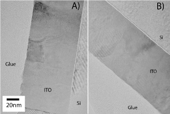
Figure 1 shows TEM images of both the as deposited and heat treated sample. Both samples are crystalline, with a layer thickness of about 80 nm. Usually ITO is amorphous when sputtered at room temperature (RT) Diplas et al. (2007), but crystalline ITO has also previously been shown to form upon deposition at room temperature Song et al. (1998, 1999a); Antony et al. (2004); Mei-Zhen et al. (2008). Crystallization may be influenced by the gas pressure and the target to sample distance. A suitable gas pressure has to be chosen so as to minimize collisions between the sputtering gas and the sputtered target atoms, and the distance between target and the sample should not be too large in order to preserve the kinetic energy of the sputtered particles. By tuning these parameters it is feasible to obtain a sufficient surface mobility of the sputtered atoms and, hence, increase nucleation sitesSong et al. (1998, 1999a); Antony et al. (2004). It is also established that crystallization of DC sputtered ITO at room temperature (RT) depends on the thickness of the sputtered film. Moreover, it has been suggested that the substrate type affects the critical thickness of the film required for crystallization Mei-Zhen et al. (2008). It is established that the crystallization temperature of ITO is of the order of 150-160∘C Song et al. (1999b); Paine et al. (1999), whilst in this work the measured sample temperature during deposition was 80∘C.
Crystalline ITO may also form by plasma enhanced crystallization. In this context the presence of crystallinity in the as deposited samples could be explained as follows. The distance between target and substrate is 8 cm. At this distance, the plasma surrounding the target also covers parts of the wafer. It is therefore possible that the crystallization of the as deposited ITO layer is enhanced by the plasma.
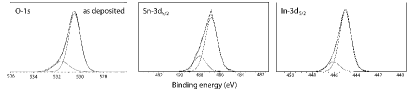
XPS was used to identify the composition and chemical state of the elements in the ITO. The XPS high resolution peaks of the O-1s, Sn-3d5/2, and In-3d5/2 for the two samples are shown in Figure 2. The O-1s spectra have been fitted with two peaks located at a binding energy of 530.5 eV and 531.8 eV. The Sn-3d5/2 spectra have been fitted with two peaks at 486.8 eV and 488.0 eV, and the In-3d5/2 at 444.9 eV and 446.0 eV; see Table 1. The peaks have been labelled as to distinguish them during discussion. The origin of the Sn and In components labelled as InII, SnII, InIII, SnIII, and will be discussed in detail in this chapter. The InI and SnI components will be discussed in Section IV. The peak positions and reference values are presented in Table 1.
The binding energies of InII and InIII are very close to the reference values for amorphous ITO and In(OH)x, respectively. However, since TEM images revealed that most of the ITO was crystalline, the InII and SnII peaks are most likely due to crystalline ITO. The two peaks have therefore been fitted with an asymmetry, due to the metallic character of ITO. The asymmetry of the peak was varied in order to see if the InIII component could only be an expression of the asymmetry of the InII component. However, fitting the spectra with only one peak did not give satisfactory peak fitting. Kim et al.Kim et al. (2003) fitted the In-3d5/2 peak with two components, located at 444.08 eV and 445.24 eV (energy separation 1.16 0.1 eV), attributed to crystalline and amorphous ITO, respectively. The energy separation between the two fitted In-3d components in this work is 1.1 eV. This indicates that the small In-3d5/2 peak at 446.0 eV may be attributed to amorphous ITO. The InII/InIII relative fractions are 90 at. % and 10 at. %, respectively. Since the SnII peak corresponds to crystalline ITO, the SnIII may be attributed to Sn in amorphous ITO. The binding energies of the OI and OII peaks fit also well with that of crystalline and amorphous ITO, respectively.
In order to fully determine the chemical state of the oxide, the electroneutrality principle was used Kim et al. (1999a). The doubly-charged O2- and singly charged OH- will have different stoichiometry when combined with the lattice cation. Substitutional Sn in the In2O3 oxide will have an (OI + OII)/(In + Sn) theoretical ratio of 1.5, while Sn interstitial will be 1.55 when the oxygen is in the form of O2- Kim et al. (1999a). If the anions in the oxide are in the form of OH- instead of O2-, the ratio will be 3.0 Kim et al. (1999a). The atomic percentages of the different elements in ITO bulk as well as their calculated ratios for the as deposited (asd) and heat treated (ht) samples are presented in Table 2. If OI, InII, and SnII correspond to crystalline ITO (with the oxygen present as O2-), the OI/(InII + SnII) ratio would be about 1.5. The actual ratio for the as deposited sample was 1.34 and for the heat treated sample 1.36. The components that may correspond to amorphous ITO have a ratio of OII/(InIII + SnIII) = 1.83 and 2.02 for as deposited and heat treated, respectively. This ratio is far higher than what is expected for amorphous ITO (about 1.5). When using the sum of all, the calculated ratios (OI + OII)/(InII + InIII + SnII + SnIII) 1.41 (asd) and 1.45 (ht), which are closer to the value for crystalline ITO. This suggest that the OI, OII, InII, InIII, SnII, and SnIII all result from crystalline ITO, and the presence of In(OH)3 is also excluded.
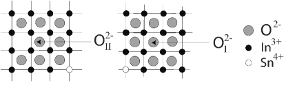
Application of the electroneutrality principle contradicts our initial assignment of the InIII, SnIII, and OII compounds. However, crystalline ITO may have contributions from both OI and OII peaks. Kim el al. Kim et al. (1999a) showed that OI and OII may originate from two different types of O2- ions (O and O); see Figure 3. It has been suggested that a double O2- peak is common for oxides containing cations in multiple valence states Kim et al. (1999a); Kichinosuke Hirokawa and Oku (1975). A higher binding energy of the O ions may be due to presence of oxygen in oxygen-deficient regions. This means that these oxygen ions do not have neighbouring In atoms with full complement of six nearest neighbour O2- ions Kim et al. (1999a); Fan and Goodenough (1977); see Figure 3. According to Fan et al.Fan and Goodenough (1977), the O peak has a about 1.5 eV higher binding energy than O. The chemical shift between the OI and OII peaks in Figure 2 is 1.3 0.1 eV. The OII peak may therefore also contain contributions from oxygen deficient regions in the ITO. As a consequence, the OII/OI ratio may be used to determine the oxygen deficiency of the material Kim et al. (1999a). This ratio is 0.2 0.1 for the as deposited and 0.2 0.1 for the heat treated sample (see Table 2). The uncertainty in the calculated oxygen deficiency ratio is 0.1, assuming an uncertainty of 0.05 at. % in the measured composition. This measured ratio is lower than what was found for bulk ITO (1.06) by Kim et al.Kim et al. (1999a) and is closer to bulk ITO made by a combination of aquaregia treatment (HNO3, HCl, and distilled water) and dry cleaning with oxygen plasma Kim et al. (1999a), which was 0.8-0.9. A lower oxygen deficiency in the film may be a result of a decreased number of oxygen vacancies Wu et al. (1994), which may result in a decreased film conductivity Kim et al. (1999b).
IV Results and Discussion of the ITO/Si interface
A detailed HRTEM, EFTEM, and XPS study of the interface is presented in the next sections, together with the effects of electron beam irradiation.
| Composition | Binding energy (eV) |
|---|---|
| InI | 444.2 |
| InII | 445.0 |
| InIII | 446.4 |
| OI | 530.6 |
| OII | 531.5 |
| OII | 532.7 |
| SnII | 484.5 |
| SnII | 486.8 |
| SnIII | 488.2 |
IV.1 Elemental composition measured using XPS
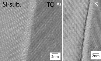
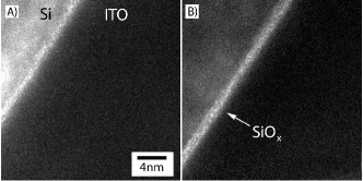
Figure 4 shows HRTEM images of the ITO/Si interface. A 2 nm amorphous layer is visible between the Si substrate and the ITO film. This interface layer is present in both the as deposited and the heat treated sample. Si readily oxidises when exposed to small amounts of O2, and SiOx is expected to form at the ITO/Si interface. When heat treated at high temperatures, this oxide has been reported to grow Ow-Yang et al. (2000) (heated at 785 ∘C for 33 min). The interface oxide seen in our samples did not grow during heat treatment. However, our sample has only been heated at 300∘C for 15 min, and this temperature is probably too low to induce further oxidation.
| Distance (nm) | |||
|---|---|---|---|
| 11.5 | 1.45 | 1.36 | 0.20 |
| 10.0 | 1.45 | 1.28 | 0.25 |
| 8.5 | 1.45 | 1.22 | 0.27 |
| 7.0 | 1.57 | 1.28 | 0.32 |
| 5.5 | 1.62 | 1.11 | 0.63 |
| 3.0 | 2.16 | 0.92 | 2.61 |
| 1.5 | 3.72 | ||
| 0.0 | 4.41 | ||
| -1.5 | 3.28 |
Ramasse et al.Ramasse et al. (2009) have studied ITO deposited on Si using chemical vapour deposition and re-annealed in vacuum for 30s at 400∘C. They identified the interfacial oxide as SiOx. EFTEM imaging of the plasmon peak of pure Si (16 eV) and SiOx (23 eV, which is very close to the plasmon peak of SiO2) was performed to confirm this. Figure 5A is filtered at 16 eV, which means that the bright areas in the image result from pure Si. Figure 5B is filtered at 23 eV. The amorphous region is bright when imaging with electrons at 23 eV. As expected, the interface oxide consists of SiOx.
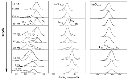
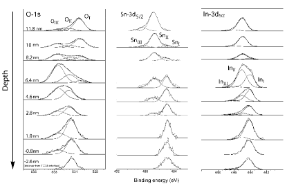
The interface composition of In, O, and Sn was examined using XPS. Figure 6 and Figure 7 show XPS spectra of the a) O-1s peak, b) Sn-3d peak, and c) In-3d5/2 peak near the ITO/Si-substrate interface of the as deposited and heat treated sample, respectively, acquired upon depth profiling using Ar+ etching. The In-3d5/2 spectra have been fitted with three components located at 444.2 eV, 445.0 eV, and 446.4 eV. The O-1s spectrum is also fitted with three components at 530.6 eV, 531.5 eV, and 532.7 eV. The Sn-3d5/2 peak has been fitted with three components located at a binding energy of 484.9 eV, 486.8 eV, and 488.2 eV. All binding energy values are presented in Table 3. The spectra from the as deposited and the heat treated sample are very similar and show that heat treatment did not have a large effect on the elemental and chemical state distribution. From the spectra in Figures 6 and 7 the atomic percentages of the different oxidation states were measured. These values are plotted in Figure 8 together with the percentage of Si0 and Six (spectra not shown).
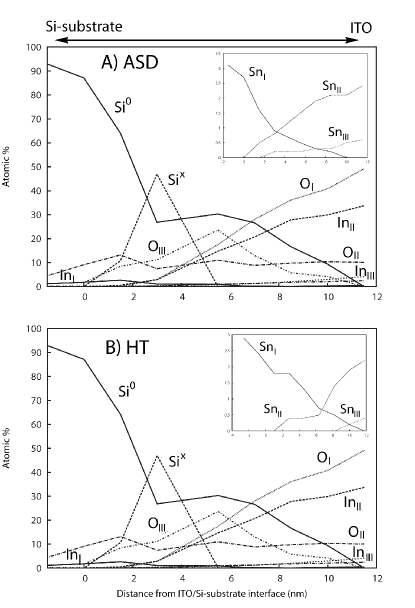
Peaks InII, InIII, SnII, SnIII, OI, and OII are due to crystalline ITO, as discussed in Section III. The binding energies of InI and SnI are similar to the litterature values for pure In and Sn, 443.7 eVZhua et al. (2000) and 485 eVKe et al. (2007), respectively. The pure In and Sn concentration increase towards the interface. If the InIII, SnIII, and OII components exist in crystalline ITO, they should show the same trend (increase or decrease). However, the intensity of the OII component increases towards the ITO/Si-substrate interface where those of InIII and SnIII ones decrease. The InIII and SnIII peaks could also not be in a composition with the OIII peak, for the same reason.
As seen from the HRTEM and EFTEM images in Figures 4 and 5, SiOx is present as a 2 nm layer near the interface. Oxygen in SiO2 has a reported binding energy of 533.05 eV Hollinger et al. (1975). The OIII peak has a binding energy of 532.7 eV and appears around the same depth as the Si-2p peak (spectra not shown). This suggests that the OIII peak results from oxygen in SiOx. The peak is present at a distance of 8 nm from the interface. This distance is more than what was identified as SiOx by TEM and EFTEM. This is because the image resolution in the TEM (0.19 nm) is far better than the depth resolution in XPS (which is the photoelectron escape depth of about 7 nm).
The electroneutrality principle was again used to determine the chemical state of the oxide close to the interface, for both the as deposited and heat treated sample. Since both TEM and XPS data show no significant differences between the two samples, only the data of the as deposited sample is presented in Table 4. The (OI+OII)/(Intotal+Sntotal) ratio is within 1.4-1.6 for the first four spectra in Figure 6. This means that the oxide probably contains mostly O2-. Towards the interface the ratio increases to around 4. This is considerably higher than what was observed for non-interfacial ITO in Section III.
As discussed in Section III, the OII/OI ratio may be used to determine the oxygen deficiency in the material Kim et al. (1999a). The oxygen ratio is presented in Table 4 for the as deposited sample. The oxygen deficiency ratio of non-interfacial ITO as presented in Section III was 0.2 and 0.21 for the as deposited and the heat treated sample, respectively. The ratio of oxygen deficient regions near the interface is higher. At 11 nm from the interface the ratio is the same as bulk for ITO film. Moving towards the interface the ratio increases, and at the interface the ratio is close to 2. These results show that there is presence of pure In0 and Sn0 at the interface, together with highly oxygen deficient regions.
The pure In and Sn at the interface have most likely formed during deposition, when oxygen from ITO may have reacted with the unsaturated Si at the wafer surface to make SiOx Diplas et al. (2010). Pure In and Sn have therefore probably been a bi-product of this reaction.
IV.2 Electron beam induced crystallization
In the previous section XPS analysis indicated that pure In and Sn co-exist with oxygen deficient regions near the interface. Since conventional TEM bright field imaging did not reveal presence of In clusters, one can assume that pure In exists as amorphous nanoclusters near the ITO/Si interface. Upon exposure to high electron beam illumination, the sample at the interface reacted with the electron beam. Figure 9 shows an HRTEM image of the as deposited sample before (A) and after (B) electron beam exposure. During electron beam illumination, small nanocrystals appear at the ITO/Si interface.
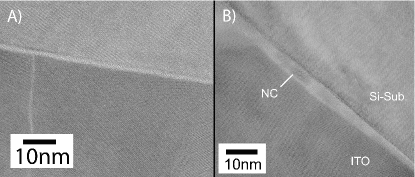
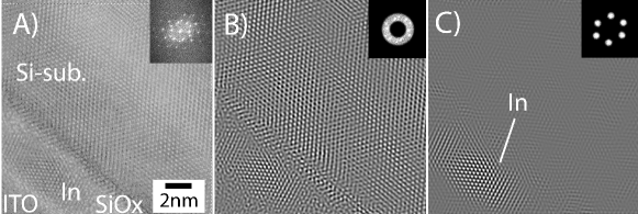
Figure 10A shows HRTEM images of the ITO/Si interface after only seconds of electron beam irradiation. After a short interval of electron irradiation, nanocrystals appear at the ITO/Si substrate interface in the interfacial oxide layer. The Fast Fourier Transformed (FFT) image inserted in the Figure, shows the diffraction pattern of both the Si substrate and the interface nanocrystal. Figure 10B shows the HRTEM image after applying a circular mask with both the Si and the interface nanocrystal diffraction pattern, while Figure 10C has resulted from applying a mask of only the diffraction patterns of the interface nanocrystal. The inserted FFT patterns in the image show the applied mask. After calibrating the diffraction pattern using the Si diffraction pattern as a reference, the lattice parameters of the interface nanocrystals were found to be 0.270 nm and 0.243 nm. In has a space group of I4/mmm (No. 139), with nm and nm Moshopoulou et al. (2006). The measured lattice parameters fit well with the (101) and (002) plane of pure In, which are 0.270 nm and 0.244 nm, respectively. Therefore, the structure of the interface nanocrystal fits well with the structure of pure In. The elemental composition near the interface as discussed in the beginning of this section was found to be composed of SiOx in addition to the presence of In and Sn nanoclusters. The TEM results strengthen the argument that pure In is present as nanoclusters. During high energy electron irradiation, the In clusters crystallize. In addition to this crystallization, the interface oxide increases in thickness from 2 nm to 5 nm (see Figure 10).
Pure In at the interface has previously been reported by Ow-Yang et al. Ow-Yang et al. (2000) and Kobayashi et al.Kobayashi et al. (1992). Kobayashi et al.Kobayashi et al. (1992) found presence of metallic In by XRD when the deposition of ITO occurred at angle. Ow-Yang et al. Ow-Yang et al. (2000) studied the ITO/Si interface by XRD and thermodynamics. Even though no other reaction product was detected by TEM at the ITO/Si interface, pure In was observed by XPS. This reaction was also found to be thermodynamically stable at 1058K, as shown belowOw-Yang et al. (2000).
The In crystallization could be attributed to localized heating at the interface or to charging produced by the electron beam. An in-situ heating experiment of the sample showed no nanocrystal formation at the ITO/Si interface. It is therefore likely that crystallization and growth of the In nanocrystals are due to direct electron beam induced splitting and re-configuration of atomic bonds. Since In is present as In3+, the electron beam might attract additional In to the interface, thereby resulting in larger In clusters. This may be assisted by the oxygen depletion at the interfacial areas and subsequently by the presence of broken In-O bonds. The crystallization may naturally occur when the In cluster reaches its critical radius. Nanocluster formation and e-beam induced crystallization may have significant implications in manipulating the ITO/Si interface at the nano-scale via a combined method of deposition and electron beam irradiation in the early stages of deposition.
V Conclusion
As deposited and heat treated ITO films made by sputter deposition were studied in detail using TEM and XPS. The samples were very similar and both crystalline. This was attributed to plasma enhanced crystallization during deposition. The non-interfacial ITO consists only of crystalline ITO. XPS depth profiling and TEM of the ITO/Si interface revealed increasing amounts of In and Sn towards the interface, as well as the presence of an SiOx layer. This interface oxide did not grow during heat treatment. Pure In was present as amorphous clusters. Close to the interface areas oxygen deficient regions were also found. During electron beam exposure of the interface, the In nanoclusters crystallize and grow. In addition, growth of the SiOx layer occurred.
References
- Xirouchaki et al. (1996) C. Xirouchaki, G. Kiriakidis, T. Pedersen, and H. Fritzsche, J. of Appl. Phys. 79, 9349 (1996).
- Kim et al. (2005) S. H. Kim, N.-M. Park, T. Kim, and G. Sung, Thin Solid Films 475, 262 (2005).
- Ando et al. (2003) M. Ando, E. Nishimura, K. Onisawa, and T. Minemura, J. of Appl. Phys. 93, 1032 (2003).
- Chopra et al. (2000) K. Chopra, S. Major, and K. Pandya, Thin Solid Films 102, 1 (2000).
- Ohta et al. (2000) H. Ohta, M. Orita, M. Hirano, H. Tanji, H. Kawazoe, and H. Hosono, Appl. Phys. Lett. 76, 2740 (2000).
- Tahar et al. (1998) R. Tahar, T. Ban, Y. Ohaya, and Y. Takahashi, J. Appl. Phys. 83, 2631 (1998).
- Kobayashi et al. (1991) H. Kobayashi, T. Ishida, Y. Nakato, and H. Tsubomura, J. Appl. Phys. 69, 1736 (1991).
- Kim et al. (2003) Y.-S. Kim, Y.-C. Park, S. Ansari, B.-S. Lee, and H.-S. Shin, Thin Solid Films 426, 124 (2003).
- Kim et al. (1999a) J. Kim, P. Ho, D. Thomas, R. Friend, F. Cacialli, and G. Bao, Chem. Phys. Lett. 315, 307 (1999a).
- Ishida et al. (1993) T. Ishida, H. Kobayashi, and Y. Nakato, J. Appl. Phys. 73, 4344 (1993).
- Fan and Goodenough (1977) J. Fan and J. Goodenough, J. Appl. Phys. 48, 3524 (1977).
- Ow-Yang et al. (2000) C. W. Ow-Yang, Y. Shigesato, and D. C. Paine, J. of Appl. Phys. 88, 3717 (2000).
- Ramasse et al. (2009) Q. Ramasse, A. Anapolsky, C. Lazik, and M. J. A. A. A. Wang, J. of Appl. Phys. 105, 033716 (2009).
- Kobayashi et al. (1992) H. Kobayashi, T. Ishida, K. Nakamura, Y. Nakato, and H. Tsubomura, J. Appl. Phys. 72, 5288 (1992).
- Zhua et al. (2000) F. Zhua, C. Huan, K. Zhang, and A. Wee, Thin Solid Films 359, 244 (2000).
- de Carvalho et al. (2000) C. N. de Carvalho, A. B. do Rego, A. Amaral, P. Brogueira, and G. Lavareda, Surface and Coatings Technology 124, 70 (2000).
- Jimenez et al. (1996) V. Jimenez, A. Fernandez, J. Espinos, and A. Gonzalez-Elipe, Surf. Sci. 350, 123 (1996).
- Ke et al. (2007) F.-S. Ke, L. Huang, J.-S. Cai, and S.-G. Sun, Electrochimica Acta 52 52, 6741 (2007).
- Peng et al. (2002) X. S. Peng, G. W. Meng, X. F. Wang, Y. W. Wang, J. Zhang, X. Liu, and L. D. Zhang, Chem. Mater. 14, 4490 (2002).
- (20) http://www.casaxps.com/.
- Diplas et al. (2007) S. Diplas, A. Ulyashin, K. Maknys, A. Gunnaes, S. Jørgensen, D. Wright, J. Watts, A. Olsen, and T. Finstad, Thin Solid Films 515, 8539 (2007).
- Song et al. (1998) P. K. Song, Y. Shigesato, I. Yasui, C. W. Ow-Yang, and D. C. Paine, Japanese J. of Appl. Phys. 37, 1870 (1998).
- Song et al. (1999a) P. K. Song, Y. Shigesato, M. Kamei, and I. Yasui, Japanese J. of Appl. Phys. 38, 2921 (1999a).
- Antony et al. (2004) A. Antony, M. Nisha, R. Manoj, and M. K. Jayaraj, Appl. Surf. Sci. 225, 294 (2004).
- Mei-Zhen et al. (2008) G. Mei-Zhen, R. Job, X. De-Sheng, and W. R. Fahrner, Chinese Phys. Lett. 25, 1380 (2008).
- Song et al. (1999b) P. K. Song, H. Akao, M. Kamei, Y. Shigesato, and I. Yasui, Japanese J. of Appl. Phys. 38, 5224 (1999b).
- Paine et al. (1999) D. C. Paine, T. Whitson, D. Janiac, R. Beresford, and C. O. Yang, J.of Appl.Phys. 85, 8446 (1999).
- Kichinosuke Hirokawa and Oku (1975) F. H. Kichinosuke Hirokawa and M. Oku, J. Elec. Spec. Rel. Phenom. 6, 333 (1975).
- Wu et al. (1994) W.-F. Wu, B.-S. Chiou, and S.-T. Hsieh, semicond. Sci. Technol. 9, 1242 (1994).
- Kim et al. (1999b) H. Kim, C. M. Gilmore, A. Pique , J. S. Horwitz, H. Mattoussi, H. Murata, Z. H. Kafafi, and D. B. Chrisey, J. of Appl. Phys. 86, 6451 (1999b).
- Hollinger et al. (1975) G. Hollinger, Y. Jugnet, P. Pertosa, and T. M. Duc, Chem. Phys. Lett. 36, 441 (1975).
- Diplas et al. (2010) S. Diplas, O. M. Lovvik, H. Nordmark, D. Kepaptsoglou, J. M. Graff, C. Ladam, F. Tyholdt, J. C. Walmsley, A. E. Gunnaes, R. Fagerberg, et al., Surf. and Inter. Anal. 42 (2010).
- Moshopoulou et al. (2006) E. G. Moshopoulou, R. M. Ibberson, J. L. Sarrao, J. D. Thompson, and Z. Fisk, Acta Crystallographica B 39, 173 (2006).