Transforming Fabry-Pérot resonances into a Tamm mode
Abstract
We propose a novel photonic structure composed of metal nanolayer, Bragg mirror and metal nanolayer. The structure supports resonances that are transitional between Fabry-Pérot and Tamm modes. When the dielectric contrast of the DBR is removed these modes are a pair of conventional Fabry-Pérot resonances. They spectrally merge into a Tamm mode at high contrast. Such behavior differs from the results for structures supporting Tamm modes reported earlier. The optical properties of the structure in the frequency range of the DBR stop band, including highly beneficial transmittivity through thick structures, are determined by the introduced in the paper hybrid resonances. The results can find a wide range of photonic applications.
pacs:
42.70.Qs, 78.55.Cr, 41.20.Jb, 42.25.Hz, 78.68.+m, 73.20.MfMetal inclusions are increasingly employed to improve the photonic performance of semiconductor devices. For example, resonant-cavity enhancement by thin metal layers has been shown to increase the quantum efficiency of novel multi-band photodetectors Lao et al. (2011). The interface between metal and distributed Bragg reflector (DBR), a configuration often encountered in optoelectronic devices, has attracted a great deal of attention since the seminal papers proposing and observing optical Tamm states Kavokin et al. (2005) and Tamm plasmons (TP) Kaliteevski et al. (2007); Sasin et al. (2010). Several developments soon followed, such as studies of hybrid optical Tamm states Brückner et al. (2011) and coupled TPs Iorsh et al. (2012). Interaction of Tamm states with excitons Symonds et al. (2009) have been observed and Tamm exciton polaritons are proposed as candidates for signal carriers in a novel type of integrated circuits Liew et al. (2010); Kaliteevski et al. (2009). TPs have been found promising for the fields of quantum optics Gazzano et al. (2011) and polaritonics Flayac et al. (2012).
In this paper we study optical properties of the metal nanolayer - DBR - metal nanolayer (MNL-DBR-MNL) structure in the spectral region of the stop band of the DBR for the first time. It is shown that the proposed structure supports modes that are intermediate between Fabry-Pérot resonances (FPRs) and a Tamm plasmon. The dependence of the modes on the dielectric contrast of the DBR is surprising in light of previous reports (e.g. Ref. [Iorsh et al., 2012]), but is very reasonable according to the given in our paper arguments. Another distinctive feature of the structure is the symmetry of the resonances. We demonstrate that magnetically symmetric resonance (i.e. electrically antisymmetric) is at low energy. The intriguing properties of the structure are achieved if the metal layers are thinner than metal skin depth, i.e. . Then at resonances the incident power is equally split between absorption and transmission. Transmission of of incident power persists until the resonances merge into a TP. Owing to the sensitivity of the modes to the thickness of the metal layers, dielectric contrast of the DBR and to the number of layers, the modes can be used to tailor response of planar metal-semiconductor devices and to control field distribution inside them.
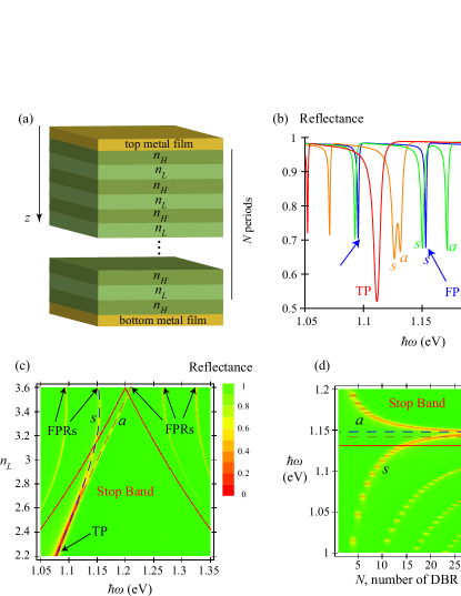
The proposed structure is composed of two identical metal films and one-dimensional array, which forms a DBR with Bragg frequency (see Fig. 1 (a)). Each of periods of the DBR is composed of a couple of dielectric layers with refraction indices and , . The thicknesses of the layers are denoted as and , making the total thickness of the DBR stack . The thickness of metal films covering the DBR is .
We follow the characteristic matrix approach Born and Wolf (1999). The tangential components and of magnetic and electric field in a planar structure can be related at locations and through the following matrix equation
| (1) |
Using the Abeles theorem Abelès (1950) we have obtained an expression for the characteristic matrix of the array
| (2) |
where and are the characteristic matrices of the and layers, are the Chebyshev polynomials of the 2nd kind, , were and are the Bloch vector and the thickness of a DBR period.
The transmission spectrum of the DBR is composed of bands of strong transmission alternating with stop bands, in which the transmission is low. In the stop bands the Bloch vector is complex and fields decay from the edges of the DBR. The decaying fields in the DBR can be matched at the metal-DBR boundary with fields penetrating the metal and form the TP modes whose intensity is enhanced at the boundary Kaliteevski et al. (2007). We consider a structure in which the DBR is bounded by metal layers from both sides. If the metal layers are thicker than the metal skin depth , i.e. , the structure supports modes with the following dispersion
| (3) |
or , where . In the paper we use a notation to denote with subscripts , , , and corresponding to the medium of incidence, metal films, and layers and substrate. Here and is the dielectric permittivity of a medium. The structures we consider are non-magnetic. In Eq. (3) the plus sign is for modes whose magnetic field is symmetric with respect to the center of the structure, and minus for antisymmetric modes. In absence of dielectric contrast in the DBR, , the modes of Eq. (3) turn into guided modes of the resulting metal-insulator-metal (MIM) structure.
Increasing the dielectric contrast of the DBR expands the stop bands and induces frequency shifts of pairs of the guided modes closest to the stop bands toward each other. This effect can be seen from Eqs. (2) and (3). The Bloch wave vector at frequencies close to the first stop band can be represented as , with being imaginary within the stop band. From the definition of Chebyshev polynomials in the limit (i.e. when field strongly decays on the length of the DBR) it follows that the matrix elements of exponentially grow such that the symmetric and antisymmetric modes of Eq. (3) become degenerate satisfying . The dispersion relation for this degenerate mode is
| (4) |
where is the component of the wave vector in layer. Excluding from Eq. (4) and definition of the Bloch vector in the range we arrive at
| (5) |
for normal incidence. With the exception of the last factor , Eq. (5) is similar to the original expression of Ref. [Kaliteevski et al., 2007] for the TP frequency. The main approximation of Ref. [Kaliteevski et al., 2007] turns out to be the assumption , resulting in error of (see Fig. 1(d)).
Thus, as the dielectric contrast of the DBR is increased in a MNL-DBR-MNL structure with thick metal films a pair of guided modes near Bragg frequency gradually become degenerate and are transformed into a TP. The splitting of TPs in a DBR bounded by two cavities with thicknesses of and semi-infinite metal layers was considered in Ref. [Iorsh et al., 2012]. The splitting for that structure grows with reduction of dielectric contrast, but then collapses at moderate contrasts according to results of Ref. [Iorsh et al., 2012], which is a very different behavior from the resonances considered in our structure.
The optical properties of the MNL-DBR-MNL structure are described by the equation:
| (6) |
where and are the reflectance and transmittance amplitudes and is the characteristic matrix of the metal films. From Eq. (6) using general relations between the characteristic and transfer matrices Furman and Tikhonravov (1992) we have obtained the analytical expressions for and . For instance, the transmittance amplitude for normal incidence is given by
| (7) |
where , and represent the Fresnel formulae, while , . We also use shorthand notations for , and . The analytical expressions were used to check the results of the numerical computations obtained by solution of Eq. (6).
In Figs. 1(b)-(d) we show computation of reflectance of a MNL-DBR-MNL structure under normal incidence. The medium of incidence and the substrate are considered as vacuum . The phenomenological parameters of gold are used for metal films Johnson and Christy (1972). Their thickness is taken which exceeds the skin depth by factor of . The DBR is formed by GaAs/GaAlAs structure. The Bragg frequency is selected to be . In this frequency range index of refraction for GaAs is , while the index of refraction of GaAlAs component physically can be in the range for different Al fraction A.N.Pikhtin and A.D.Yas’kov (1980). For the sake of argument we vary from to in this paper.
In absence of the dielectric contrast , and Eq. (7) transforms into the expression for transmission through a Fabry-Pérot resonator Born and Wolf (1999). In MNL-DBR-MNL structures with low dielectric contrast the transmittance is high (and reflectance is low) at Fabry-Pérot resonances, while all the incident radiation is reflected at other frequencies. In Fig. 1(b) we show the reflectance spectrum . The structure for which (blue curve) has three FPRs in the frequency range shown (marked by arrows) separated by equal frequency bands of strong reflection. If the index of refraction is lowered to (green curve) one of the FPRs corresponding to a magnetically antisymmetric mode (marked by ) is strongly shifted to the red. The symmetric mode at lower frequency (marked by ) is not shifted, which leads to reduced separation between the modes. At (orange curve) the reflection dips corresponding to the symmetric and antisymmetric modes are separated by . The energies of the modes fully merge at as shown by the red curve and correspond to the energy of TP.
The transformation of the modes is further demonstrated in Fig. 1(c). This panel shows the dependence of the reflectance spectrum on the dielectric contrast (i.e. on ). The stop band lower and upper frequencies are shown by the red curves (they formally limit the frequency band with ). At high dielectric contrast the MNL-DBR-MNL structure fully reflect the incident radiation except for the narrow band marked as TP. As the dielectric contrast is reduced this reflection dip is split into two dips, which become FPRs at low contrast. We show the dispersion of the modes [Eq. (3)] by the dashed lines. They follow the reflectance dips obtained using Eq. (6). The correspondance of the reflection dips to the modes of Eq. (3) is due to the fact that considerably exceeds the skin depth . At high dielectric contrast the modes described by Eq. (3) merge and follow the dispersion of the TP given by Eq. (4).
The Tamm plasmon splitting as the contrast of the DBR is reduced is due to reduction of and hybridization of TPs localized at different metal-DBR boundaries. Along the same lines the splitting should be observed if the number of periods of the DBR is reduced at constant contrast (i.e. ). This is confirmed by the Fig. 1(d). If one can see a single reflectance dip at the bottom of the stop band due to the excitation of the TP. The dashed blue line corresponds to the energy of TP calculated using Eq. (4). The dashed brown line is at the energy of TP calculated using expression of Ref. [Kaliteevski et al., 2007] (the discrepancy of about ). For this dip is split into two dips with higher frequency separation between them for smaller , reaching for the structure with .
If the thickness of the metal layers is smaller than , the frequencies of the reflection dips cannot be described by Eqs. (3) and (4). In Fig. 2(a) we show computations similar to those shown in Fig. 1(c), but for . A considerable shift to the red of both resonances compared to the modes in the structure with thick metal films (dashed lines) is observed. Reflectance reduction at the resonances is much stronger than in the case with . This is due to the enhanced interaction of incident radiation with the resonances for . The resonances are strongly excited leading to higher field intensity in the structure and increased transmittance.
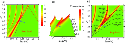
In Figs. 2(b)-(c) we plot the transmittance of the same MNL-DBR-MNL structure as in Fig. 2(a). The transmittance is highly suppressed in the frequency band under consideration, except for the strong transmittance peaks at the resonances, corresponding to the dips in reflectance. It can be seen that at lower contrast, when the transmittance peaks are split, the maximum transmittance is , while reflectance is , which allows to estimate the absorbance by both modes as .
The resonances merge if the dielectric contrast of the DBR is increased. The merger point, which corresponds to , is marked by the blue arrows in all panels of Fig. 2. For even stronger dielectric contrast the transmittance decays exponentially as can be clearly seen from Fig. 2(b). This decay can be understood from Fig. 2(c), in which the transmittance is superimposed on the lines of constant (the dashed black lines). As the contrast is increased the frequency of the modes correspond to higher value of this parameter, for instance, for . From Eq. (7) one can see that for higher contrast . This implies that optical fields become exponentially weak on the bottom side of the structure with consequent diminishing of transmittance. We will show below that decay of transmittance is due to destructive interference between the resonant modes on the bottom side of the DBR.
Consider a structure with inversion symmetry such that . The tangential magnetic and electric field components can be represented as sums of even and odd functions with respect to the center of the structure, e.g. as , where . Both symmetric and antisymmetric terms represent solutions of Maxwell equations for the structure. Therefore, Eq. (6) is partitioned as:
| (8) |
where index () corresponds to plus (minus) sign, so that and . In Eq. (8) . All of the spectral characteristics of the structure with inversion symmetry are determined by the reflection amplitudes and for the magnetically symmetric and antisymmetric parts of the field.
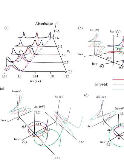
The absorbance spectra of the same structure as in Fig. 2 are shown in Fig. 3(a). In Fig. 3(a) we plot the total absorbance (black curves) as well as partial absorbances of the symmetric (red curves) and antisymmetric (blue curves) field components. The absorbance peaks in Fig. 3(a), which are in agreement with reflectance dips and transmittance peaks of Fig. 2. Using the partial absorbances and coefficients and the lower energy peak can be attributed to the resonance of the magnetically symmetric part of the field, while the higher energy peak is related to the antisymmetric part of the field. As was mentioned above at low dielectric contrast the absorbance for both modes is . When the peaks of partial absorbances merge the total absorbance increases, which corresponds to the exponential decay of the transmittance (cf. Figs. 2(b)-(c)).
In Fig. 3(b)-(d) we show the frequency dependences of complex parameters (red curve), (blue curve) and the total reflectance amplitude (green curves). In panel (b) the structure with moderate dielectric contrast () is considered. At lower frequencies both parts of the field are non-resonant, so that and all of the incident power is reflected for both field symmetries. At the symmetric part of the field becomes resonant, which can be seen by the loop of the red curve in Fig. 3(b). At the antisymmetric part of the field is resonant and the blue curve makes a resonance loop. Both loops are well separated in frequency, which results in two separate loops of , two dips of reflectance (cf. Fig. 2(a)) and two peaks of transmittance (cf. Figs. 2(b)-(c)) and absorbance (cf. Fig. 3(a)). In the midst of the resonances the reflection coefficients are phase-shifted by with respect to the incident waves. The phase of the total reflection coefficient varies within the range from to .
Increasing the contrast (see Fig. 3(c) for and Fig. 3(d) for ) results in reduction of splitting between symmetric and antisymmetric resonances. Correspondingly, the loops that and make in the complex plane as functions of frequency occur at closer frequencies, which changes the shape of the curve corresponding to the total reflectance coefficient . Instead of the two frequency-separated loops, makes a heart-shaped loop at with a small sub-loop that corresponds to the increase in reflectance between closely placed dips in the spectrum shown in Fig. 2(a). At the two resonances merge and the loops coincide in Fig. 2(d). The curve for contains only one loop resulting in the single dip in reflectance spectrum in Fig. 2(a). The phase of the total reflection coefficient is in the middle of the resonance. Due to the reduced splitting between the resonances the loops of and approach each other in Figs. 3(b)-(d), which leads to exponential decay of the transmittance shown in Figs. 2(b)-(c).
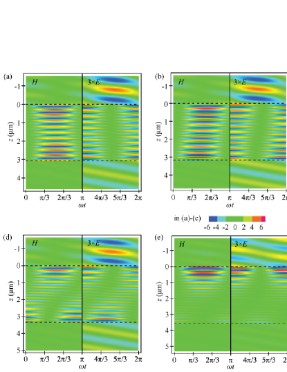
In Fig. 4 we show the field distribution during an oscillation period for several situations. In panels (a)-(e) the magnetic field is shown for the first half of the period, while electric field is shown for the second half. The graphs correspond to normal incidence, therefore the field is not modulated perpendicularly to the growth axis. Off-resonance incidence upon the structure leads to full reflection of radiation, without considerable field intensity penetrating the structure itself. If the incident radiation excites the symmetric field resonance as shown in Fig. 4(a), the field penetrates into the structure. The character of the field distribution in Fig. 4(a) confirms that the symmetric resonance is excited. The parameters pertaining to the panels of Fig. 4 are marked in Fig. 2(c).
In Fig. 4(b) excitation of an antisymmetric resonance is demonstrated. In this case the magnetic field is out of phase on different sides of the structure. One can also notice that there is a small delay of the field oscillations on the upper side of the structure with respect to the field at the bottom. This is due to admixture of the symmetric mode to mainly antisymmetric field distribution. At the dielectric contrast is already high enough for the symmetric and antisymmetric modes to be spectrally close and interfere. High degree of interference is shown in Fig. 4(c) for excitation at a frequency between the symmetric and antisymmetric resonances (see Fig. 2(c)). The field is enhanced at the bottom of the structure and suppressed at the top, which corresponds to exponential growth of the field towards the bottom of the structure.
Interference in the structure can be also seen in Fig. 4(d) at the merger point of the symmetric and antisymmetric modes. Both modes are strongly excited and interfere to produce field distributions which are localized on one side of the structure and decay towards another side with the localization side being alternated after a quarter of the optical period. After the full merger of the resonances the modes destructively interfere on the bottom side of the structure as shown in Figs. 4(e)-(f). The field decays exponentially towards the back side of the structure, which results in exponential decay of transmission as was discussed in relation with Figs. 2(b)-(c). The power that is not transmitted is dissipated in the top metal film instead, which is represented in Fig. 3(a) by increased absorbance when the splitting between the symmetric and antisymmetric resonances is small.
In summary, we have shown that optical properties of the metal nanolayer - DBR - metal nanolayer structure in the frequency range near the stop band of the DBR are determined by a pair of resonances which are intermediate between Fabry-Pérot resonances at low dielectric contrast of the DBR and a Tamm plasmon at high contrast. We have demonstrated that in a MNL-DBR-MNL structure with inversion symmetry the low energy resonance corresponds to a resonance of field part, which is symmetric in magnetic field, while the antisymmetric part has a higher energy resonance. The spectral merger of these resonances leads to appearance of a Tamm plasmon and considerable decrease of transmission as well as enhanced absorption. In moderate and high contrast structures the resonances are weakly split, which allows for various spatio-temporal interference patterns and opens possibility for coherent control in the proposed structure.
References
- Lao et al. (2011) Y.-F. Lao, G. Ariyawansa, and A. G. U. Perera, Journal of Applied Physics 110, 043112 (2011).
- Kavokin et al. (2005) A. V. Kavokin, I. A. Shelykh, and G. Malpuech, Physical Review B 72, 233102 (2005).
- Kaliteevski et al. (2007) M. Kaliteevski, I. Iorsh, S. Brand, R. A. Abram, J. M. Chamberlain, A. V. Kavokin, and I. A. Shelykh, Physical Review B 76, 165415 (2007).
- Sasin et al. (2010) M. E. Sasin, R. P. Seisyan, M. A. Kaliteevski, S. Brand, R. A. Abram, J. M. Chamberlain, I. V. Iorsh, I. A. Shelykh, A. Y. Egorov, A. P. Vasil’ev, et al., Superlattices and Microstructures 47, 44 (2010).
- Brückner et al. (2011) R. Brückner, M. Sudzius, S. I. Hintschich, H. Fröb, V. G. Lyssenko, and K. Leo, Physical Review B 83, 033405 (2011).
- Iorsh et al. (2012) I. Iorsh, P. Panicheva, I. Slovinskii, and M. Kaliteevski, Technical Physics Letters 38, 351 (2012).
- Symonds et al. (2009) C. Symonds, A. Lemaitre, E. Homeyer, J. C. Plenet, and J. Bellessa, Applied Physics Letters 95, 151114 (2009).
- Liew et al. (2010) T. C. H. Liew, A. V. Kavokin, T. Ostatnicky, M. Kaliteevski, I. A. Shelykh, and R. A. Abram, Physical Review B 82, 033302 (2010).
- Kaliteevski et al. (2009) M. Kaliteevski, S. Brand, R. A. Abram, I. Iorsh, A. V. Kavokin, and I. A. Shelykh, Applied Physics Letters 95, 251108 (2009).
- Gazzano et al. (2011) O. Gazzano, S. M. de Vasconcellos, K. Gauthron, C. Symonds, J. Bloch, P. Voisin, J. Bellessa, A. Lemaitre, and P. Senellart, Physical Review Letters 107, 247402 (2011).
- Flayac et al. (2012) H. Flayac, G. Pavlovic, M. A. Kaliteevski, and I. A. Shelykh, Physical Review B 85, 075312 (2012).
- Born and Wolf (1999) M. Born and E. Wolf, Principles of Optics (University Press, Cambridge, 1999).
- Abelès (1950) F. Abelès, Ann. de Physique 5, 777 (1950).
- Furman and Tikhonravov (1992) S. Furman and A. Tikhonravov, Basics of optics of multilayer systems (Editions Frontiers, Gif-sur Yvette, 1992).
- Johnson and Christy (1972) P. B. Johnson and R. W. Christy, Physical Review B 6, 4370 (1972).
- A.N.Pikhtin and A.D.Yas’kov (1980) A.N.Pikhtin and A.D.Yas’kov, Soviet Physics - Semiconductors 14, 389 (1980).