A topological crystalline insulator phase via topological phase transition and crystalline mirror symmetry
Abstract
A topological insulator protected by time-reversal symmetry is realized via spin-orbit interaction driven band inversion. The topological phase in the Bi1-xSbx system is due to an odd number of band inversions. A related spin-orbit system, the Pb1-xSnxTe, has long been known to contain an even number of inversions based on band theory. Here we experimentally investigate the possibility of a mirror symmetry protected topological crystalline insulator phase in the Pb1-xSnxTe class of materials which has been theoretically predicted to exist in its end compound SnTe. Our experimental results show that at a finite-Pb composition above the topological inversion phase transition, the surface exhibits even number of spin-polarized Dirac cone states revealing mirror-protected topological order distinct from that observed in Bi1-xSbx. Our observation of the spin-polarized Dirac surface states in the inverted Pb1-xSnxTe and their absence in the non-inverted compounds related via a topological phase transition provide the experimental groundwork for opening the research on novel topological order in quantum devices.
Topological insulators are band insulators featuring uniquely spin-polarized surface states, which is believed to be a consequence of odd number of inversions of bulk bands driven by spin-orbit interaction alone or in combination with crystal lattice modulations Moore ; RMP ; Zhang_RMP ; Hasan QPT ; Matthew Nature physics BiSe . The odd number of band inversion transitions in the bulk demarcate a Z2 topological insulator phase with spin-polarized surface states from that of a conventional band insulator phase as previously demonstrated in topological insulator Bi1-xSbx and the Bi2Se3 series Moore ; RMP ; Zhang_RMP ; Hasan QPT ; Matthew Nature physics BiSe . Within band theoretical calculations, lead tin telluride Pb1-xSnxTe, which is a narrow band-gap semiconductor widely used for infrared optoelectronic and thermoelectric devices PbTe IR ; PbTe Thermal , has long been known to contain an even number of band inversions as electronic structure is tuned via the Sn/Pb ratio PST band-gap ; PST Inversion1 ; PST Inversion2 ; PST Inversion3 ; Volkov ; Fradkin . Theoretical calculations have also predicted the occurrence of surface or interface states within the inverted band-gap upon the band inversion transition PST Inversion3 ; Volkov ; Fradkin but no experimental evidence of the surface states has been reported so far. Recent theoretical works Liang PRL TCI ; Liang NC SnTe have further stimulated the experimental search for surface states in Pb1-xSnxTe. In a recent calculation Liang NC SnTe , Hsieh et al. predicted that the topological surface states in SnTe Liang NC SnTe are protected by crystalline space group symmetries, in contrast to the time-reversal symmetry protection in the well known Z2 topological insulators.
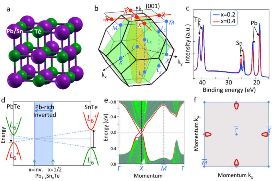
The crystal group symmetry of Pb1-xSnxTe, critical for the realization of the topological crystalline insulator (TCI) phase Liang PRL TCI , is based on the sodium chloride structure (space group Fmm (225)). In this structure, each of the two atom types (Pb/Sn, or Te) forms a separate face-centered cubic lattice, with the two lattices interpenetrating so as to form a three-dimensional checkerboard pattern. The first Brillouin zone (BZ) of the crystal structure is a truncated octahedron with six square faces and eight hexagonal faces. The band-gap of Pb1-xSnxTe is found to be a direct gap located at the points in the BZ PST band-gap ., which are the centers of the eight hexagonal faces of the BZ. Due to the inversion symmetry of the crystal, each point and its diametrically opposite partner on the BZ are completely equivalent. Thus there are four distinct point momenta. It is well established that the band inversion transitions in the Pb1-xSnxTe take place at these four points of the BZ PST Inversion1 ; PST Inversion2 ; PST Inversion3 ; Volkov ; Fradkin . As a result, even number of (four) inversions exclude the system from being a Kane-Mele Z2 topological insulator RMP . However, it is interesting to note that the momentum-space locations of the band inversions coincident with the momentum-space mirror plane within the BZ. This fact provides a clue that band inversions in Pb1-xSnxTe may lead to a distinct topologically nontrivial phase that is irrelevant to the time-reversal symmetry but may be the consequence of the spatial mirror symmetries of the crystal, which has been theoretically shown in the inverted end compound SnTe Liang NC SnTe . However, it is experimentally known that SnTe crystals actually subject to a rhombohedral distortion PST Rhombohedral Distortion , which, strictly speaking, breaks the crystal mirror symmetries and hence excludes a gapless TCI phase Liang NC SnTe . More importantly, SnTe crystals are typically heavily p-type SnTe p-type due to the fact that Sn vacancies are thermodynamically stable SnTe p-type , which makes the chemical potential of SnTe to lie below the bulk valence band maximum, consequently not cutting across the surface states. The surface states, which may exist within the band-gap, are thus unoccupied and cannot be experimentally studied by photoemission experiments SnTe ARPES . On the other hand, the Pb-rich samples are reported to possess the ideal (averaged) sodium chloride structure without global rhombohedral distortion PST Rhombohedral Distortion which thus preserve the proper crystal symmetry required for the predicted TCI phase Liang NC SnTe . Moreover, it is possible to grow Pb-rich crystals, in which the chemical potential can be brought up above the bulk valence band maximum (in-gap or even n-type) PST n-type so as to lie near the surface state Dirac point.
Therefore, in order to experimentally investigate the possibility of a topological phase transition, and thus rigorously proving the existence of a TCI phase in the Pb1-xSnxTe system, we hereby utilize angle-resolved photoemission spectroscopy (ARPES) and spin-resolved ARPES to study the low energy electronic structure below and above the band inversion topological transition in the Pb-rich compositional range of the system, through which the observation of spin-polarized surface states in the inverted regime and their absence in the non-inverted regime is demonstrated, correlating the observed spin-polarized Dirac surface states with the expected band inversion topological phase transition. We further map out the critically important spin structure of the surface states protected by mirror symmetries in the inverted topological composition. These results show that the topological order observed in Pb1-xSnxTe is distinct from that previously discovered in Bi1-xSbx or Bi2Se3 Moore ; RMP ; Zhang_RMP ; Hasan QPT ; Matthew Nature physics BiSe . Our spin-resolved study of Pb1-xSnxTe paves the way for further investigation of many novel properties of topological crystalline order Liang PRL TCI ; Yannopapas ; Wang ; Vildanov in real materials and devices.
Results
Comparison of non-inverted and inverted compositions
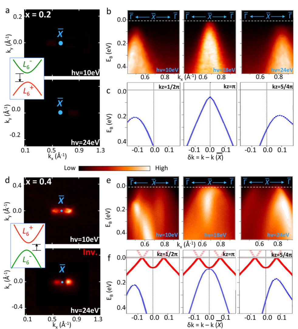
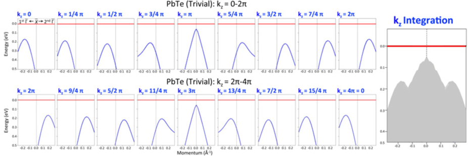
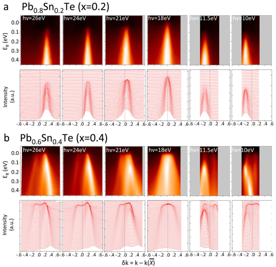
In order to capture the electronic structure both below and above the band inversion transition (theoretically predicted to be around PST Inversion1 ; PST Inversion2 ), we choose two representative compositions, namely and , for detailed systematic studies. Figure 1c shows the momentum-integrated core level photoemission spectra for both compositions, where intensity peaks corresponding to tellurium , tin , and lead orbitals are observed. The energy splitting of the Pb orbital is observed to be larger than that of the Sn orbital, which is consistent with the stronger spin-orbit coupling of the heavier Pb nuclei. In addition, the spectral intensity contribution of the Sn peaks in the sample (red) is found to be higher than that of in the sample (blue), which is also consistent with the larger Sn concentration in the samples. We perform systematic low energy electronic structure studies on these two representative compositions. Since the low energy physics of the system is dominated by the band inversion at points ( points projected onto points on the (001) surface), we present ARPES measurements with the momentum space window centered at the point, which is the midpoint of the surface BZ edge (see Fig. 1b). Figure 2a,b show the ARPES Fermi surface and dispersion mappings of the Pb0.8Sn0.2Te sample (). The system at is observed to be gapped: No band is observed to cross the Fermi level in the Fermi surface maps (Fig. 2a). The dispersion measurements (Fig. 2b) reveal a single hole-like band below the Fermi level. This single hole-like band is observed to show strong dependence with respect to the incident photon energy (see Fig. 2b, and also detailed in Supplementary Figures S1-S3 and Supplementary Methods in the supplementary information (SI).), which reflects its three-dimensionally dispersive bulk valence band origin. As a qualitative guide to the ARPES measurements on , we present first-principles based electronic structure calculation on the non-inverted end compound PbTe (Fig. 2c). Our calculations confirm that PbTe is a conventional band insulator, whose electronic structure can be described as a single hole-like bulk valence band in the vicinity of each point, which is consistent with our ARPES results on Pb-rich Pb0.8Sn0.2Te. The three-dimensional nature of the calculated bulk valence band is revealed by its evolution in Figure 2c, which is in qualitative agreement with the incident photon energy dependence of our ARPES measurements shown in Figure 2b.
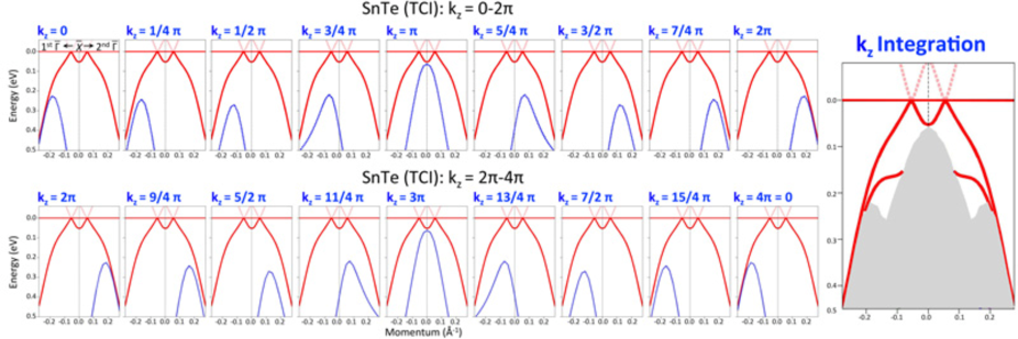
Now we present comparative ARPES measurements under identical experimental conditions and setups on the Pb0.6Sn0.4Te () sample. In contrast to the conventional band insulator (insulating) behavior in the sample, the Fermi surface mapping (Fig. 2d) on the sample shows two unconnected metallic Fermi pockets (dots) on the opposite sides of the point. Such two-pockets Fermi surface topology cannot be easily interpreted as the bulk valence band since the low energy bulk valence band of the Pb1-xSnxTe system is a single hole-like band, unless certain surface-umklapp processes of the bulk states are considered, which usually have only weak cross-section in ARPES measurements. The assignment of the observed two-Fermi-pockets as surface-umklapp processes or other bulk-related origins can be further ruled out by incident photon energy dependence ( dispersion) measurements and our spin polarization studies of these metallic states (see Supplementary Figures S1-S5 in the SI). The dispersion measurements on the sample are shown in Figure 2e. The single hole-like bulk valence band, which is similar to that in the sample, is also observed below the Fermi level. More importantly, a pair of metallic states crossing the Fermi level on the opposite sides of the point is observed along the mirror line momentum space direction. These states are found to show no observable dispersion upon varying the incident photon energy (further details in Supplementary Figure S3), reflecting its two-dimensional character. On the other hand, the single hole-like band is observed to disperse strongly upon varying the incident photon energy, suggesting its three-dimensional character. At a set of different photon energy () values, the bulk valence band intensity overlaps (intermixing) with different parts of the surface states in energy and momentum space. At a photon energy of 18 eV, the intermixing (intensity overlap) is strong, and the inner two branches of the surface states are masked by the bulk intensity. At photon energies of 10eV and 24 eV, the surface states are found to be relatively better isolated. These ARPES measurements suggest that the sample lie on the inverted composition regime and that the observed surface states are related to the band inversion transition in Pb1-xSnxTe as predicted theoretically PST Inversion3 ; Volkov ; Fradkin ; Liang NC SnTe . As a qualitative guide, we present first-principles based electronic structure calculation on the inverted end compound SnTe (Fig. 2f). The calculated electronic structure of SnTe is found to be a superposition of two nondispersive metallic surface states and a single hole-like dispersive bulk valence band in the vicinity of the point, which is in qualitative agreement with the ARPES results on Pb0.6Sn0.4Te.
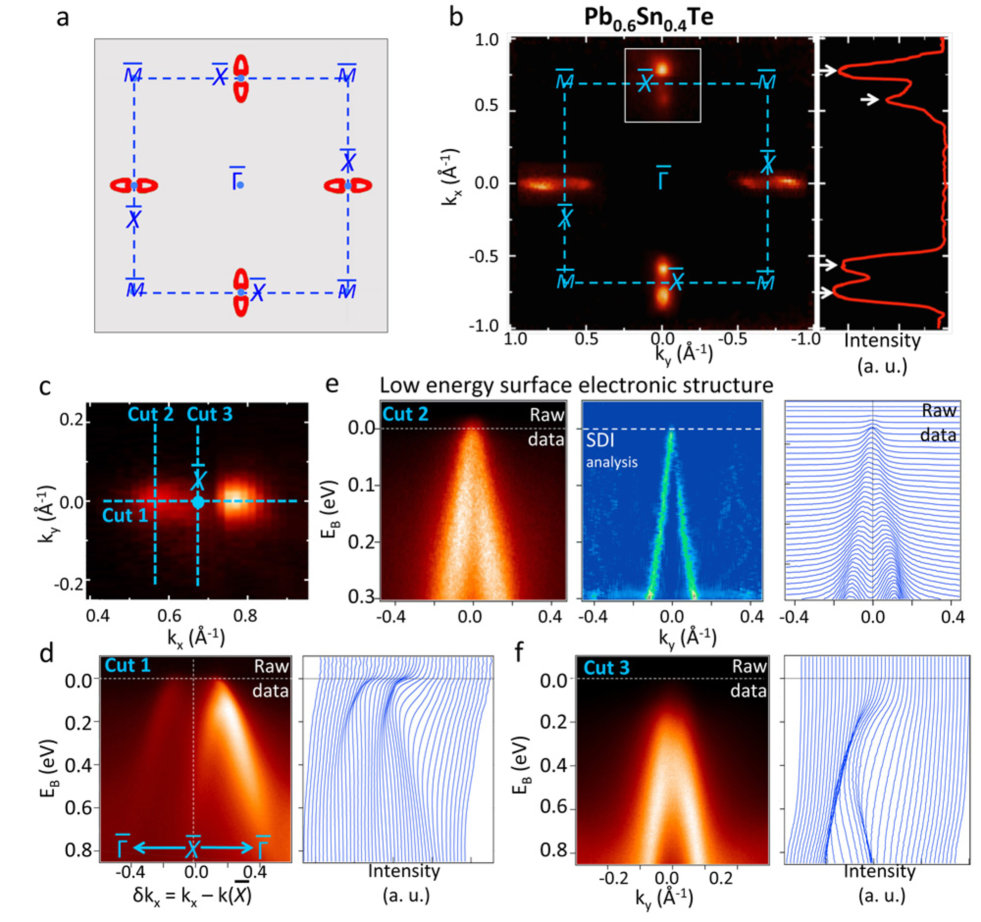
Surface state topology of Pb0.6Sn0.4Te
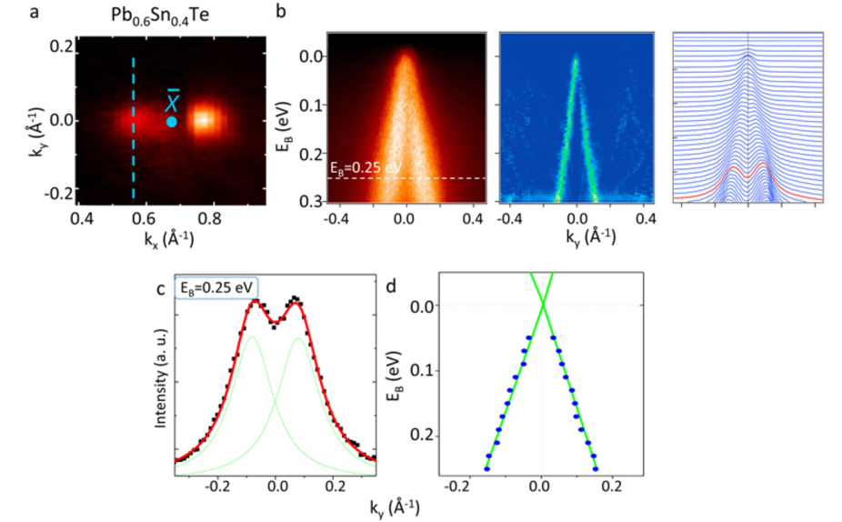
We now perform systematic measurements on the surface electronic structure of the Pb0.6Sn0.4Te. Figure 3b shows the wide range Fermi surface mapping covering the first surface BZ. The surface states are observed to be present, and only present, along the mirror line () directions. No other states are found along any other momentum directions on the Fermi level. In close vicinity to each point, a pair of surface states are observed along the mirror line direction. One lies inside the first surface BZ while the other is located outside. Therefore, in total four surface states are observed within the first surface BZ, in agreement with the fact that there are four band inversions in Pb1-xSnxTe. The mapping zoomed-in near the point (Fig. 3c) reveals two unconnected small pockets (dots). The momentum space distance from the center of each pocket to the point is about . Dispersion measurements ( vs ) are performed along three important momentum space cuts, namely cuts 1, 2, and 3 defined in Fig. 3b, in order to further reveal the electronic structure of the surface states. Metallic surface states crossing the Fermi level are observed in both cuts 1 and 2, whereas cut 3 is found to be fully gapped, which is consistent with the theoretically calculated surface states electronic structure shown in Figure 1e. In cut 1 (Fig. 3d), which is the mirror line () direction, a pair of surface states are observed on the Fermi level. The surface states in our Pb0.6Sn0.4Te samples are found to have a relatively broad spectrum, which can be possibly understood by the strong scattering in the disordered alloy system similar to the broad spectrum of the topological surface states in the Bi1-xSbx alloy David Nature BiSb . In addition to the scattering broadening, the surface states are also observed to tail on the very strong main valence band emission (for example, the white region of intensity distribution in Fig. 3d). In the case of Figure 2e (photon energy of 24 eV), the bulk valence band maximum (VBM) locates outside the first surface BZ. The surface state inside the first surface BZ is relatively better isolated from the bulk bands as compared to the one outside the first surface BZ. We thus study the dispersion along cut 2 (Fig. 3d), which only cuts across the surface states inside the first surface BZ. Both the dispersion maps and the momentum distribution curves in cut 2 reveal that the surface states along cut 2 are nearly Dirac-like (linearly dispersive) close to the Fermi level. In many topological insulators, the surface states deviate from ideal linearity Liang PRL Warping . Fitting of the momentum distribution curves of cut 2 (see Supplementary Figure S6 for data analysis) shows that the experimental chemical potential () lies roughly at (or just below) the Dirac point energy (), eV. The surface states’ velocity is obtained to be ( m/s) along cut 2, and ( m/s) for the two outer branches along cut 1, respectively.
Spin polarization measurements of the surface states
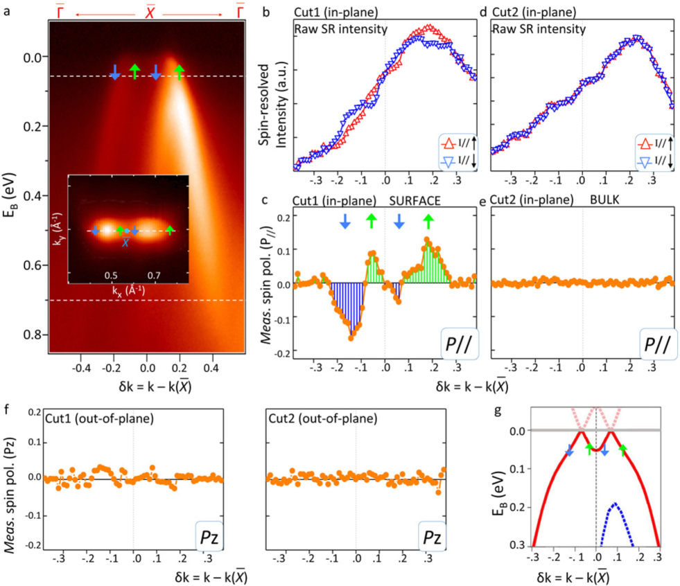
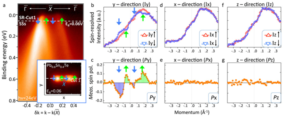
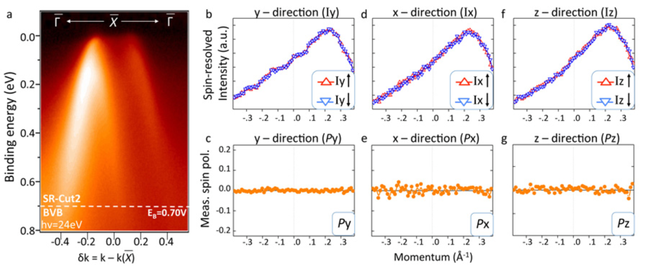
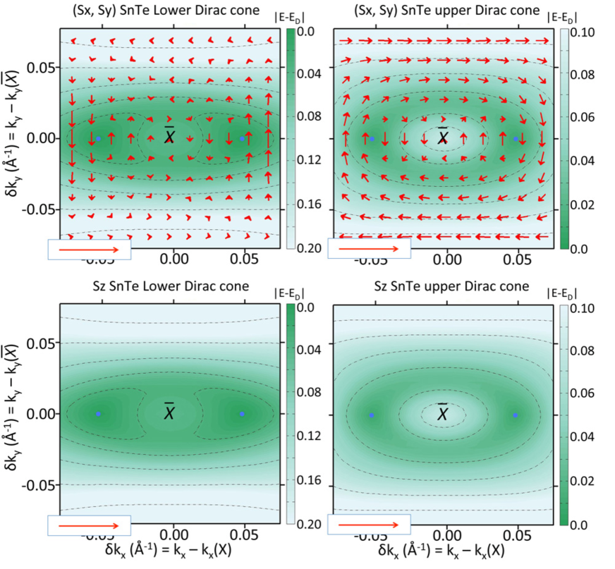
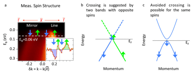
We study the spin polarization of the low energy states of the Pb0.6Sn0.4Te samples, which are highly dominated by the surface states near the Fermi level. We further compare and contrast their spin behavior with that of the states at high binding energies away from the Fermi level, which are highly dominated by the bulk valence band in the same sample. Spin-resolved (SR) measurements are performed in the spin-resolved momentum distribution curve mode Spin1 ; Spin2 , which measures the spin-resolved intensity and net spin polarization at a fixed binding energy along a certain momentum space cut direction (detailed in the Methods section). As shown in Figure 4a, our spin-resolved measurements are performed along the mirror line () direction, since the electronic and spin structure along this direction is most critically relevant to the predicted TCI phase Liang NC SnTe . Considering that the natural Fermi level of our samples are very close to the Dirac point (which is spin degenerate), the spin polarization of the surface states are measured at 60 meV below the Fermi level in order to gain proper contrast, namely SR-Cut 1 in Figure 4a. As shown in the net spin polarization measurement of SR-Cut 1 in Figure 4c, in total four spins pointing in the () in-plane tangential direction are revealed for the surface states along the mirror line direction. This is well consistent with the observed two surface state cones (four branches in total) near an point along the mirror line direction. To compare and contrast the spin polarization behavior of the surface states (SR-Cut 1) with that of the bulk states, we perform spin-resolved measurement SR-Cut 2 at eV, where the bulk valence bands are prominently dominated. Indeed, in contrast to SR-Cut 1 reflecting the surface states’ spin polarization, no significant net spin polarization is observed for SR-Cut2, which is expected for the bulk valence bands of the inversion symmetric (centrosymmetric) Pb1-xSnxTe system. Our observed spin polarization configuration of the surface states is also in qualitative agreement with the first-principles calculation spin texture of the SnTe TCI surface states (see Supplementary Figures S7-S9 for texture calculation). And Experimental derived topological invariant (Mirror Chern number Mirror Chern Number ; David Science BiSb ) also agrees with theoretical prediction for SnTe Liang NC SnTe .
Discussion
We discuss the possibility that the observed surface states in our data are the signature of the theoretically predicted TCI phase. The TCI phase was predicted to be observed in the band inverted side and absent in the non-inverted side Liang NC SnTe . In our data of the Pb0.6Sn0.4Te samples which lie on the inverted side, surface states are observed, and only observed, along the two independent mirror line () directions. Within the first surface BZ, two surface states are observed on each mirror line, which are found to locate in vicinity of the points. Dispersion measurements (e.g. Cut 2 in Fig. 3) reveal a nearly linear dispersion. Spin polarization measurements show that these surface states are spin-polarized and their spin polarization direction is locked with their momentum (spin-momentum locking). The overall electronic structure observed for our surface states are in qualitative agreement with the theoretically predicted surface states of the TCI phase in SnTe Liang NC SnTe . It is important to note that in an alloy, the space group symmetry is only of the averaged type. The spatial mirror symmetry required for the topological protection is only preserved in a globally averaged sense. To this date, it is not even theoretically known whether only averaged mirror symmetry is sufficient for the predicted TCI phase. In the absence of any theoretical work for the alloy, the experimental proof of mirror protection in the alloy Pb1-xSnxTe(Se) system perhaps requires the observation of strictly gapless surface states. The current ARPES works PSS TCI ; PST Xu have not demonstrated resolution better than 5 meV, and thus fitting of the energy-momentum distribution curves lacks the resolving power to exclude gap values less than 5 meV (demonstrated in Supplementary Figure S10 and Supplementary Discussion). On the other hand, a proof of strictly gapless surface states in fact requires a surface and spin sensitive experimental setup with energy resolution better than 1 meV, which can even exclude possible small gap values of meV at the Dirac point. Even a gap size of even less than 1 meV can lead to observable change in spin-transport experiments, thus destroying the delicate TCI phase. Therefore, while the existence of surface states correlated with band inversion transition is established here in our work, their gapped or gaplessness nature requires surface transport experiments on samples with improved quality, which is currently not possible PSS TCI .
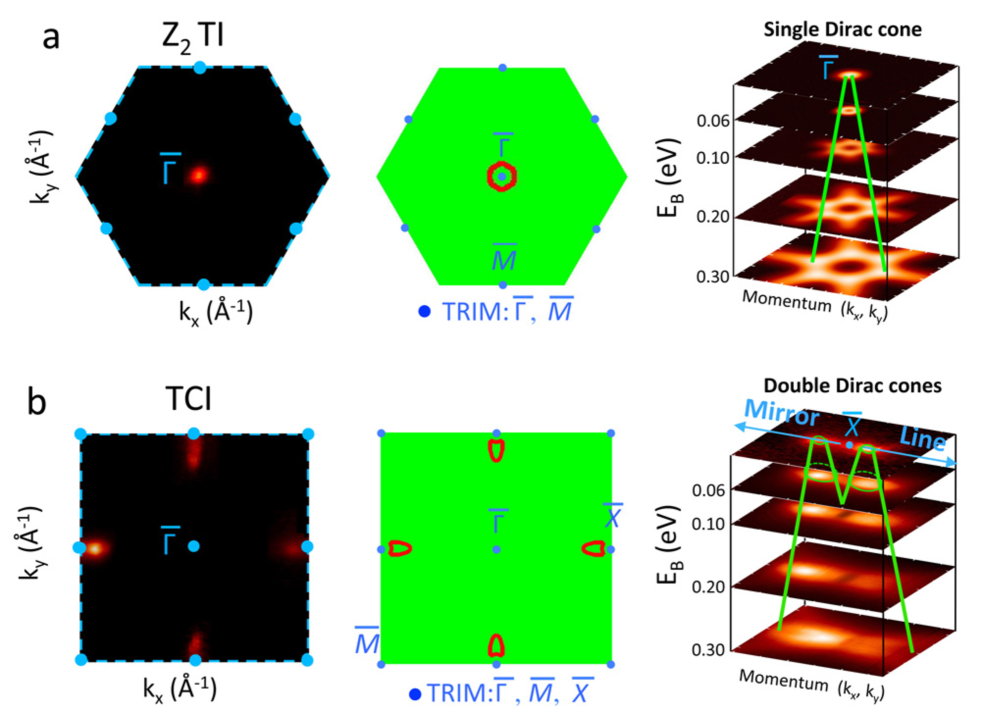
Our observations of spin-momentum locked surface states in the inverted composition and their absence in the non-inverted composition suggest that Pb1-xSnxTe system is a tunable spin-orbit insulator analogous to the BiTl(S1-δSeδ)2 system Hasan QPT , which features a topological phase transition across the band inversion transition. However, the key difference is that odd number of band inversions in the BiTl(S1-δSeδ)2 system leads to odd number of surface states, whereas even number of band inversions in Pb1-xSnxTe system leads to even number of surface states per surface BZ. We further present a comparison of the Pb0.6Sn0.4Te and a single Dirac cone Z2 topological insulator (TI) GeBi2Te4 Ternary arXiv ; Ternary PRB ; Kimura . As shown in Figure 5a-c, for GeBi2Te4, a single surface Dirac cone is observed enclosing the time-reversal invariant (Kramers’) momentum in both ARPES and calculation results, demonstrating its Z2 topological insulator state and the time-reversal symmetry protection of its single Dirac cone surface states. On the other hand, for the Pb0.6Sn0.4Te samples (Fig. 5d-f), none of the surface states is observed to enclose any of the time-reversal invariant momentum, suggesting their irrelevance to the time-reversal symmetry related protection. With future ultra-high-resolution experimental studies to prove the strict gapless nature of the Pb0.6Sn0.4Te surface states and therefore the topological protection by the crystalline mirror symmetries, it is then possible to realize magnetic yet topologically protected surface states in the Pb1-xSnxTe system due to its irrelevance to the time-reversal symmetry related protection, which is fundamentally not possible in the Z2 topological insulator systems. Considering the wide applications of magnetic materials in modern electronics, such topologically protected surface states compatible with magnetism will be of great interest in terms of integrating topological insulator materials into future electronic devices.
We note that one advantage of the Pb1-xSnxTe system is that it can be easily doped with manganese, thallium, or indium to achieve bulk magnetic or superconducting states PbMnTe ; Tl-PbTe ARPES ; In-SnTe Ando . The symmetry in the Pb1-xSnxTe system (its nonmagnetic character) can be broken by magnetic or superconducting doping into the bulk or the surface. In future experiments, it would be interesting to explore the modification of our observed surface states brought out by magnetic and superconducting correlations, in order to search for exotic magnetic and superconducting order on the surface. Such magnetic and superconducting orders on the surface states in Pb1-xSnxTe can be different from those recently observed in the Z2 topological insulators Andrew CuBiSe ; Hedgehog due to its very distinct topology of surface electronic structure. The novel magnetic and superconducting states to be realized with this novel topology are not strongly related to the question of gapless or gapped nature of the TCI phase. Therefore our observation of the spin-polarized surface states presented here provides the much desired platform for realizing unusual surface magnetic and superconducting states in future experiments.
Methods
Electronic structure measurements.
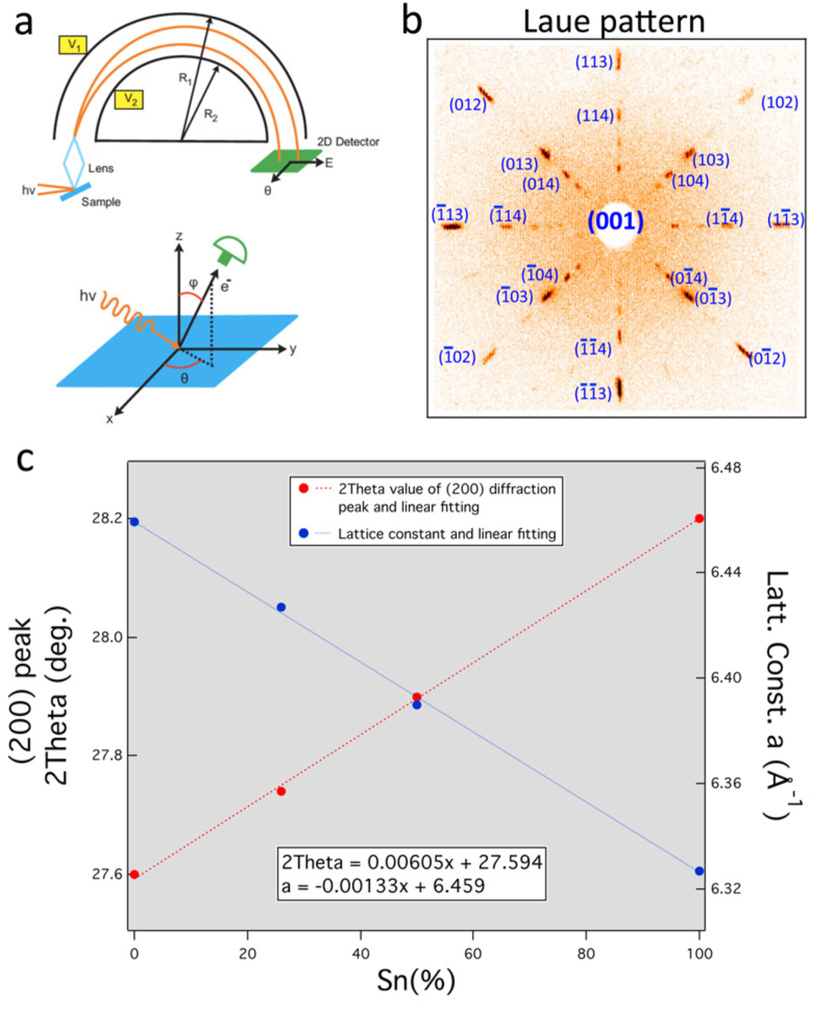
Spin-integrated angle-resolved photoemission spectroscopy (ARPES) measurements were performed with incident photon energies of eV to eV at beamline 5-4 at the Stanford Synchrotron Radiation Lightsource (SSRL) in the Stanford Linear Accelerator Center, and with eV to eV photon energies at beamlines 4.0.3, 10.0.1, and 12.0.1 at the Advance Light Source (ALS) in the Lawrence Berkeley National Laboratory (LBNL). Samples were cleaved in situ between to K at chamber pressure better than torr at both the SSRL and the ALS, resulting in shiny surfaces. Energy resolution was better 15 meV than and 1% of the surface BZ. In order to cross-check the cleavage surface orientation in ARPES measurements, the Laue back-reflection x-ray measurements were performed at the ALS using a Realtime Laue delay-line detector from Multiwire Laboratories (Ithaca, NY) and diffraction spot indexing was performed using the MWL NorthStar orientation package. The x-ray Laue measurements along with the analysis results are presented in the Supplementary Figure S11.
Spin-resolved measurements. Spin-resolved ARPES measurements were performed on the SIS beamline at the Swiss Light Source (SLS) using the COPHEE spectrometer with two 40kV classical Mott detectors and a photon energy of 24 eV, which systematically measures all three components of the spin of the electron (, , and ) as a function of its energy and momentum Spin1 ; Spin2 . Energy resolution was better than 60 meV and 3% of the surface BZ for the spin-resolved measurements. Samples were cleaved in situ at 20 K at chamber pressure less than torr. Typical electron counts on the detector reach , which places an error bar of approximately for each point on our measured polarization curves.
Sample growth. Single crystals of Pb1-xSnxTe were grown by the standard growth method (described in Ref. Growth for the end compound PbTe). High purity (99.9999%) elements of lead, tin, and tellurium were mixed in the right ratio. Lead was etched by CH3COOH+H2O2 (4:1) to remove the surface oxide layer before mixing. The mixture was heated in a clean evacuated quartz tube to 924 where it was held for two days. Afterwards, it was cooled slowly, at a rate of in the vicinity of the melting point, from the high temperature zone towards room temperature. The nominal concentrations were estimated by the Pb/Sn mixture weight ratio before the growth, in which the two representative compositions presented in the paper were estimated to be and . The concentration values were re-examined on the single crystal samples after growth using high resolution x-ray diffraction measurements by tracking the change of the diffraction angle (the 2Theta angle) of the sharpest Bragg peak, from which we obtained and (see Supplementary Figure S12 for diffraction data). In the paper we note the chemical compositions as Pb0.8Sn0.2Te and Pb0.6Sn0.4Te.
First-principles calculation methods. We perform first-principles calculations to extract both the electronic structure and the spin texture of the SnTe surface states. Our first-principles calculations are within the framework of the density functional theory (DFT) using full-potential projected augmented wave method PAW as implemented in the VASP package PBE . The generalized gradient approximation (GGA) VASP is used to model exchange-correlation effects. The spin-orbital coupling (SOC) is included in the self-consistent cycles. The surfaces are modeled by periodically repeated slabs of 33-atomic-layer thickness, separated by 13-angstrom-wide vacuum regions, using a Monkhorst-Pack -point mesh over the Brillouin zone (BZ) with 208 eV cutoff energy. The room-temperature crystal structures of SnTe in ideal sodium chloride are used to construct the slab in order to have the required crystal structure and mirror symmetries required for the predicted TCI phase Liang NC SnTe (The rhombohedral distortion is found to only occur in the Sn-rich compositions () and only at low temperature PST Rhombohedral Distortion ). The experimental lattice constants of SnTe with the value of 6.327 Å are used LSalts . The experimental lattice constant of PbTe with the value of 6.46 Å LSalts in ideal sodium chloride lattice are used in the PbTe band structure calculation.
References
- (1) Hasan, M. Z. & Moore, J. E. Three-Dimensional Topological Insulators. Ann. Rev. Cond. Mat. Phys. , 55-78 (2010).
- (2) Hasan, M. Z. & Kane, C. L. Topological insulators. Rev. Mod. Phys. , 3045-3067 (2010).
- (3) Qi, X. -L. & Zhang, S. -C. Topological insulators and superconductors. Rev. Mod. Phys. , 1057-1110 (2011).
- (4) Xia, Y. et al. Observation of a large-gap topological-insulator class with a single Dirac cone on the surface. Nature Phys. , 398-402 (2009).
- (5) Xu, S. -Y. et al. Topological phase transition and texture inversion in a tunable topological insulator. Science , 560-564 (2011).
- (6) Zogg, H., Fach, A., Masek, J. & Blunier, S. Photovoltaic lead-chalcogenide on silicon infrared sensor arrays. Opt. Eng. , 1440-1449 (1994).
- (7) Zhu, P. W. et al. Thermoelectric properties of PbTe prepared at high pressure and high temperature. J. Phys.: Condens. Matter , 11185-11188 (2002).
- (8) Dimmock, J. O. & Wright, G. B. Band Edge Structure of PbS, PbSe, and PbTe. Phys. Rev. , 821-830 (1964).
- (9) Dimmock, J.O., Melngailis, I. & Strauss, A.J. Band structure and laser action in PbxSn1-xTe. Phys. Rev. Lett. , 1193-1196 (1966).
- (10) Gao, X. & Daw, M. S. Investigation of band inversion in (Pb,Sn)Te alloys using ab initio calculations. Phy. Rev. B , 033103 (2008).
- (11) Pankratov, O. A., Pakhomov, S. V. & Volkov, B. A. Supersymmetry in heterojunctions: Band-inverting contact on the basis of Pb1-xSnxTe and Hg1-xCdxTe. Solid State Commun. , 93-96 (1987).
- (12) Volkov, B. A. & Pankratov, O. A. Two-dimensional massless electrons in an inverted contact. JETP Lett. , 178-181 (1985).
- (13) Fradkin, E., Dagotto, E. & Boyanovsky, D. Physical Realization of the Parity Anomaly in Condensed Matter Physics. Phys. Rev. Lett. , 2967-2970 (1986).
- (14) Fu, L. Topological Crystalline Insulators. Phys. Rev. Lett. , 106802 (2011).
- (15) Hsieh, H. et al. Topological Crystalline Insulators in the SnTe Material Class. Nature Comm. , 982 (2012).
- (16) Iizumi, M. et al. Phase Transition in SnTe with Low Carrier Concentration. J. Phys. Soc. Jpn. , 443-449 (1975).
- (17) Burke, Jr., J. R., Allgaier, R. S., Houston, Jr., B. B., Babiskin, J. & Siebenmann, P. G. Shubnikov-de Haas effect in SnTe. Phys. Rev. Lett. , 360-361 (1965).
- (18) Littlewood, P. B. et al. Band structure of SnTe studied by Photoemission Spectroscopy. Phys. Rev. Lett. , 086404 (2010).
- (19) Takafuji Y. & Narita S. Shubnikov-de Haas Measurements in N-Type Pb1-xSnxTe. Jpn. J. Appl. Phys. , 1315-1322 (1982).
- (20) Yannopapas, V. Gapless surface states in a lattice of coupled cavities: A photonic analog of topological crystalline insulators. Phys. Rev. B , 195126 (2011).
- (21) Hao, N., Zhang, P. & Wang, Y. Topological phases and fractional excitations of the exciton condensate in a special class of bilayer systems. Phys. Rev. B , 155447 (2011).
- (22) Vildanov, N. M. Effective field theory description of topological crystalline insulators. Preprint at http://arXiv.org/abs/1205.3560 (2012).
- (23) Hsieh, D. et al. A topological Dirac insulator in a quantum spin Hall phase. Nature , 970-974 (2008).
- (24) Fu, L. Hexagonal warping effects in the surface states of the topological insulator Bi2Te3. Phys. Rev. Lett. , 266801 (2009).
- (25) Hoesch, M. et al. Spin-polarized Fermi surface mapping. J. Electron Spectrosc. Relat. Phenom. , 263-279 (2002).
- (26) Dil, J. H. et al. Spin and angle resolved photoemission on non-magnetic low-dimensional systems. J. Phys. Condens. Matter , 403001 (2009).
- (27) Teo, J. C. Y., Fu, L. & Kane, C. L. Surface states and topological invariants in three-dimensional topological insulators: Application to Bi1-xSbx. Phys. Rev. B , 045426 (2008).
- (28) Hsieh, D. et al. Observation of Unconventional Quantum Spin Textures in Topological Insulators. Science , 919-922 (2009).
- (29) Dziawa, P. et al. Topological crystalline insulator states in Pb1-xSnxSe. Preprint at arXiv:1206.1705v1
- (30) Xu, S. -Y. et al. Observation of Topological Crystalline Insulator phase in the lead tin chalcogenide Pb1-xSnxTe material class. Preprint at http://arXiv.org/abs/1206.2088 (2012).
- (31) Xu, S. -Y. et al. Discovery of several large families of Topological Insulator classes with backscattering-suppressed spin-polarized single-Dirac-cone on the surface. Preprint at http://arXiv.org/abs/1007.5111 (2010).
- (32) Neupane, M. et al. Topological surface states and Dirac point tuning in ternary topological insulators. Phys. Rev. B , 235406 (2012).
- (33) Okamoto, K. et al. Observation of a Highly Spin Polarized Topological Surface State in GeBi2Te4. Preprint at http://arXiv.org/abs/1207.2088 (2012).
- (34) Story, T. et al. Carrier-concentration-induced ferromagnetism in PbSnMnTe. Phys. Rev. Lett. , 777-779 (1986) .
- (35) Nakayama, K., Sato, T., Takahashi, T. & Murakami, H. Doping Induced Evolution of Fermi Surface in Low Carrier Superconductor Tl-Doped PbTe. Phys. Rev. Lett. , 227004 (2008).
- (36) Sasaki, S. et al. Odd-Parity Pairing and Topological Superconductivity in a Strongly Spin-Orbit Coupled Semiconductor. Preprint at http://arXiv.org/abs/1208.0059 (2012).
- (37) Wray, L. A. et al. Observation of topological order in a superconducting doped topological insulator. Nature Phys. , 855-859 (2010).
- (38) Xu, S.-Y. et al. Hedgehog spin texture and Berry’s phase tuning in a magnetic topological insulator. Nature Phys. , 616-622 (2012).
- (39) Nugraha, K. Suto, O. Itoh, J. Nishizawa, Y. Yokota, Growth and electrical properties of PbTe bulk crystals grown by the Bridgman method under controlled tellurium or lead vapor pressure. J. Cryst. Gr. , 402-407 (1996).
- (40) Kresse, G. & Joubert, D. From ultrasoft pseudopotentials to the projector augmented-wave method. Phys. Rev. B , 1758-1775 (1999).
- (41) Perdew, J. P., Burke, K. & Ernzerhof, M. Generalized Gradient Approximation Made Simple. Phys. Rev. Lett. , 3865-3868 (1996).
- (42) Kresse, G. & Hafner, J., Ab initio molecular dynamics for open-shell transition metals. Phys. Rev. B , 13115-13118 (1993).
- (43) Bis, R. F & Dixon, J. R. Applicability of Vagard’s Law to the PbxSn1-xTe Alloy System. J. Appl. Phys. , 1918-1921 (1969).
- (44) Bouad, N. et al. Neutron powder diffraction study of strain and crystallite size in mechanically alloyed PbTe. J. Solid State Chem. , 189-195 (2003).
- (45) Ishida, A., Aoki, M. Fujiyasu, H. Sn diffusion effects on x-ray diffraction patterns of Pb1-xSnxTe-PbSeyTe1-ysuperlattices. J. Appl. Phys. , 797-801 (1985).
- (46) Yakimova, R. T., Trifonova, E. P., Karagiozov, L. & Petrov, S. Structural and electrical characteristics of iodidely synthesized Pb1-xSnxTe crystals. S. Cryst. Res. Technol. , K109-K112 (1984).
- (47) Scheer, M., McCarthy, G., Seidler, D. & Boudjouk, P. North Dakota State Univ., Fargo, ND, USA., ICDD Grant-in-Aid (1994).
- (48) Hsieh, D. et al. A tunable topological insulator in spin helical Dirac transport regime. Nature , 1101-1105 (2009).
Correspondence and requests for materials should be addressed should be addressed to M.Z.H. (Email: mzhasan@princeton.edu).
Supplementary Information:
Observation of a topological crystalline insulator phase and topological phase transition in Pb1-xSnxTe
Su-Yang Xu, Chang Liu, N. Alidoust, M. Neupane, D. Qian, I. Belopolski, J. D.
Denlinger, Y. J. Wang, H. Lin, L. A. Wray, G. Landolt, B. Slomski, J. H. Dil, A.
Marcinkova, E. Morosan, Q. Gibson, R. Sankar, F. C. Chou, R. J. Cava,
A. Bansil, and M. Z. Hasan
This file includes:
| Supplementary Figures |
| Supplementary Discussion |
| Supplementary Methods |
| Supplementary References |
Supplementary Figures
Supplementary Discussion
-
-
•
The topological distinction between TI and TCI phases
-
–
TCI vs. TI / Even vs. Odd number of band inversions: It is important to note that the Pb1-xSnxTe system contains an even number of inversions [9]. Traditionally even number of band inversions are believed to be topologically trivial, and only odd number of inversions are believed to give rise to topological insulator states [2]. For this reason, although the Pb1-xSnxTe system has long been known to contain an even number of inversions, they were believed to be trivial insulators. (see Ref. [2]). Since the much studied Z2 TIs can only be realized via odd number of inversions, thus the even number inversions in the SnTe system determines that such system is topologically distinct from both the TI phase and the trivial band insulator phase, which means TCI is a new phase of topological matter.
-
–
Irrelevance of Time-Reversal Symmetry Protection: The topological distinction between TCI and TI can be directly seen from our ARPES measured surface states. For example, Fig. 5 in the maintext shows an ARPES comparison between a Z2 (Kane-Mele) TI GeBi2Te4 and our new Pb0.6Sn0.4Te samples. As shown in Fig. 5 of the maintext, GeBi2Te4 belongs to the well-understood single Dirac cone topological insulator, which is topologically the same as the famous Bi2Se3 or Bi2Te3 systems. GeBi2Te4 has only one surface state (odd number), which is found to enclose the time-reversal invariant momenta (TRIM) or the Kramers point (the point). For this reason, the single Dirac cone surface state in GeBi2Te4 (also Bi2Se3, Bi2Te3, and all other Z2 TI systems) is topologically protected by time-reversal symmetry. In sharp contrast, in the Pb0.6Sn0.4Te system, none of the surface states are found to enclose any of the time-reversal invariant momenta (TRIM). Thus the surface states in the Pb0.6Sn0.4Te system are irrelevant to time-reversal symmetry type of protection. The topological protection in the case of Pb0.6Sn0.4Te is a result of the mirror (spatial) symmetries of the crystal, as theoretically predicted by Ref. [15]. One relevant experimental evidence for the mirror protection is that all of the observed surface states are located on the mirror line momentum space directions ().
-
–
-
•
Spin polarization, Dirac crossing and gapless nature
Here we provide one experimental observation relevant to the Dirac crossing and gapless nature: the spin polarization profile. As shown in Supplementary Figure 10, for two electronic bands with opposite spin directions, crossing is the only fate. The avoided crossing and gap behavior is only allowed if the bands have the same spin flavor or they are spin degenerate. Here we show that at energy level 60 meV below the chemical potential (thus about meV around the Dirac point), the two branches of each surface state cone show the expected opposite spin directions. It has been recently experimentally shown that the spin texture of the Dirac surface states will be strongly disturbed when a gap is opened at the Dirac point [38]. The energy scale where the spin texture is disturbed roughly corresponds to the gap value [38]. Therefore, by showing a helical spin structure at about meV around the Dirac point in Supplementary Figure 4c and Supplementary Figure 10a, we can safely exclude a gap value of meV. However, whether there is a 10 meV gap or not in our surface states still need further studies.
Supplementary Methods
-
•
Laue measurements
The surface cleavage termination is determined by X-ray diffraction measurements on the cleaved samples after ARPES measurements. Supplementary Figure 11b shows a representative Laue measurement on the Pb0.6Sn0.4Te () sample. The Miller indices are noted for the diffraction peaks in Laue pattern, which reveals that the cleavage surface of the crystal is perpendicular to the [001] vertical crystal axis. The (001) surface termination determined here from Laue results is consistent with the four-fold symmetry of the ARPES Fermi surfaces and the size of the surface BZ in ARPES measurements.
-
•
X-ray diffraction measurements
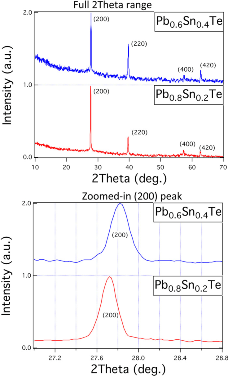
As shown in Supplementary Figure 12 for our XRD measurements on the two representative compositions, the 2Theta values of the (200) Bragg peak are found to be 27.73 deg (for the nominal concentration samples, noted as Pb0.8Sn0.2Te in the maintext) and 27.83 deg (for the nominal concentration samples, noted as Pb0.6Sn0.4Te in the maintext). Using the linear fitting above, these 2Theta values correspond to x values of (for the nominal concentration samples) and (for the nominal concentration samples). In the paper we note the chemical compositions as Pb0.8Sn0.2Te and Pb0.6Sn0.4Te.
-
•
Incident photon energy dependence study on Pb1-xSnxTe
As a qualitative guide to the ARPES incident photon energy dependence measurements, here we show the first-principles calculated bulk bands dispersion of the two end compounds inverted SnTe (Supplementary Figure 1) and non-inverted PbTe (Supplementary Figure 2) respectively.
Now we present comparative incident photon energy dependence studies between the inverted Pb0.6Sn0.4Te samples and the non-inverted Pb0.8Sn0.2Te samples under the identical experimental conditions and setups (beamline, incident photon energy values, incident light polarization, sample surface preparation procedure, etc.) as shown in Supplementary Figure 3. A pair of surface states without observable dispersion is observed in the inverted samples but absent in the non-inverted samples. no surface state on the Fermi level is observed for all the incident photon energy applied under the same experimental conditions and setups as shown in Supplementary Figure 3a. The evolution (dispersion) of the bulk valence band at different values (different incident photon energies) is in qualitative agreement with the theoretical calculation results shown above. The incident photon energy range from 26 eV to 10 eV shown in Supplementary Figure 3 corresponds to a wide range from to , which corresponds to going from the top of the bulk BZ to the center of the bulk BZ.
-
•
Fitting results of the experimental chemical potential with respect to the Dirac point energy
We apply a linear fitting to the ARPES dispersion near the Fermi level along Cut 2 in the maintext, which enables us to extract the velocity of the surface states, as well as the chemical potential () with respect to the Dirac point energy ().
-
–
Supplementary Figure 6a shows the Fermi surface mapping zoomed-in in the vicinity of an point. The blue dotted line defines a momentum space cut direction (which is the same as Cut 2 in Fig. 3 of the maintext).
- –
- –
-
–
We fit the MDCs by two Lorentzian peaks. We take the MDC Lorentzian fitting at eV as an example, as shown in Supplementary Figure 6c. The Lorentzian peak position reveals the momentum location of each branch of the Dirac surface states at eV.
-
–
By performing such fitting at different binding energies, we obtain the dispersion of the surface states, namely (, ). The solid blue circles in Supplementary Figure 6E show the obtained dispersion data points of the surface states from eV to eV with a binding energy step of eV.
-
–
Then we fit the surface states’ dispersion data points by a linear function. For the two branches of the surface state cone we obtain the following: for the branch with positive slope, we have . And for branch with negative slope, we have . Thus, the linear fittings of both branches give the velocity (the absolute value of the slope) of the Dirac cone to be around . The Dirac point energy is given by the binding energy intercept () of the linear fitting, which is 0.008 eV and -0.010 eV for each fitting respectively. This means the Dirac point energy implied by the fitting of the positive slope branch is 0.008 eV below the chemical potential , whereas the Dirac point energy implied by the fitting of the negative slope branch is 0.010 eV above the chemical potential .
-
–
In the maintext, we report a surface state velocity of along this momentum space cut direction (Cut 2 in Fig. 3 of the maintext). Furthermore the chemical potential with respect to the Dirac point is found to be eV
-
–
-
•
Spin-resolved measurements on Pb0.6Sn0.4Te
Here we show systematic spin dataset of these measurements for all three components of the spin polarization vector. The , directions for spin polarization vectors are defined in the inset of Supplementary Figure 4a. And the direction follows the right-hand rule. The , and measurements for SR-Cut 1 and SR-Cut 2 are shown in Supplementary Figure 4 and Supplementary Figure 5. As discussed in the main paper, in total four in-plane tangential () spins are revealed by these polarization measurements (Supplementary Figure 4c) on the surface states. We note that the magnitude of the spin polarization is between , which is smaller than the typically observed 40% net spin polarization of the Z2 topological insulator surface states David Nature tunable . In fact the spin polarization in our samples is found to be consistent with the first-principles based spin texture calculation on SnTe surface states (see below). As shown in Supplementary Figure 4c, the polarization magnitude of the inner two branches are found to be smaller as compared to that of the outer two branches. This can be understood by two independent reasons: First, since the inner two branches are close to each other in momentum space, their polarization signal can intermix with each other due to the finite momentum resolution of the spin-resolved measurements (the momentum resolution is about 3% of the surface BZ which corresponds to roughly ). Second, the smaller polarization of the inner two branches is even observed in our calculation on SnTe (see below). This effect is related to the anisotropy of the surface states and the hybridization of the two adjacent Dirac cones.
-
•
Spin texture calculation of SnTe
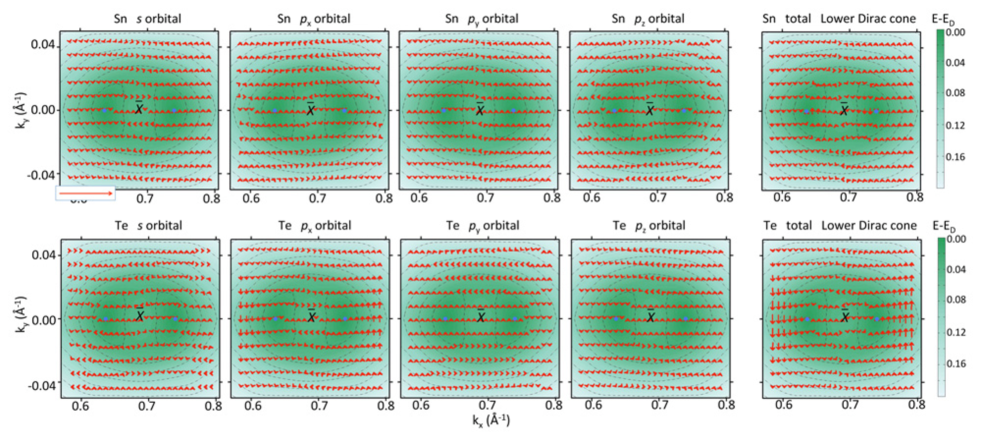
The spin texture of SnTe is calculated using VASP first-principles method. We have assumed the SnTe lattice in ideal sodium chloride structure without rhombohedral distortion. The calculated spin texture of the SnTe surface states is shown in Supplementary Figure 7 for the lower and upper Dirac cone, respectively. The out-of-plane component of the spin texture is found to be zero. We compare the calculated spin texture with the spin polarization measurements shown above: Along the mirror line direction ( in Supplementary Figure 7a), both theoretical calculations in Supplementary Figure 7a (low Dirac cone) and spin measurements in Supplementary Figure 4c reveal in total 4 spins with alternating directions in going along the mirror line. The magnitude of the spin polarization in calculation is found to range to , which is consistent with the experiments in Supplementary Figure 4c. The inner two spins close to the point are found to have smaller polarization as compared to the outer two, which is also in agreement with the experimental results in Supplementary Figure 4c.
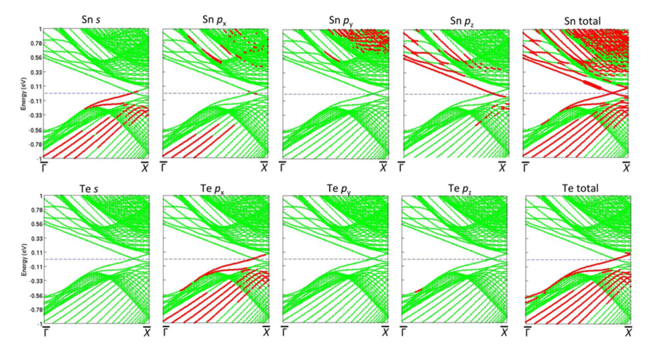
In order to better understand the spin texture, we also calculate the atomic orbital contribution of the spin texture. For the (001) surface, as shown in Supplementary Figure 9.