Topological Insulating States in Laterally Patterned Ordinary Semiconductors
Abstract
We propose that ordinary semiconductors with large spin-orbit coupling (SOC), such as GaAs, can host stable, robust, and tunable topological states in the presence of quantum confinement and superimposed potentials with hexagonal symmetry. We show that the electronic gaps which support chiral spin edge states can be as large as the electronic bandwidth in the heterostructure miniband. The existing lithographic technology can produce a topological insulator (TI) operating at temperature . Improvement of lithographic techniques will open way to tunable room temperature TI.
pacs:
72.25.Hg,73.43.-f,73.21.Cd,72.80.EyA topological insulator (TI) is a fascinating state of matter which presents unusual physical properties such as a quantum Spin Hall effect in two-dimensions (2D), spin-polarized chiral Dirac surface states in three-dimensions (3D), exotic magneto-electric effects, and Majorana fermions in the presence of superconductivity zhang ; hasankane ; moore . Although TIs have attracted a lot of attention, progress in this area has been hindered by the absence of experimental systems with robust electronic and structural properties. Although these materials have been christened as “topologically protected”, material issues associated the weak strength of the SOC, the small size of the gaps, and the strong disorder (of the order of the electronic bandwidth) present in most of the proposed systems, make the experimental realization of these amazing physical properties very difficult, if not unattainable.
One of the first theoretical predictions for such TI states was made for graphene Kane05 in the early days of graphene research Greview . Nevertheless, carbon is a light element with weak intrinsic SOC ( eV). In addition, in flat graphene, due to wavefunction orthogonality, the SOC for the -bands is even weaker ( eV) and, therefore, essentially unobservable. While deviations from flat sp2, to out of plane sp3, bonds can lead to three fold enhancement of the SOC netoguinea , the atomic control over these deformations is a major experimental challenge. Shortly after its initial proposal, TI states where predicted to occur in HgTe quantum wells hgte , in 3D bulk solids of binary compounds involving Bi biti , and half-Heusler ternary compounds hsinlin . Unfortunately, all these materials are very sensitive to stoichiometry. Hence, the unavoidable presence of defects, which are usually unitary scatterers and can act as donors/acceptors, has a strong effect in the electronic structure. One observes, for instance, large broadening of the spectral lines for surface states in angle resolved photo-emission, and doping of the bulk crystal ultimately transforming the TIs into metals kanemoore .
An idea to use semiconductors to produce TI was put forward in Ref. Liu . In particular it was suggested to use inverted InAs/GaSb Quantum Wells. The system was realized experimentally with some indications for helical edge modes knez . In this paper, we propose an alternative way to produce robust, structurally stable, and tunable TI states in ordinary semiconductors such as GaAs. The advantages of these materials are that they have significant SOC, they can be grown with extreme precision using molecular beam epitaxy (MBE) with large electronic mobilities, they can be tailored into quantum wells with arbitrary thickness, and can be controlled by external gates socreview . The robustness and flexibility of these systems can be the starting point for the creation of different kinds of TIs that cannot be obtained otherwise.
In fact, it is known that hole-doped zinc-blend semiconductors naturally have large SOC that originates from the atomic fine structure splitting. We demonstrate that the effective SOC in a semiconductor quantum well with a superimposed hexagonal superlattice can be controlled by the strength of the transverse confinement and the scale of the superlattice. Hence, the SOC gap can made comparable to the bandwidth or continuously switched to zero. Finally, we show that the SOC leads to the appearance of chiral spin edge modes in contrast with systems such as graphene where these edge states exist even in the absence of SOC Gedge . Thus, in our proposal, the system can be continuously tuned between the Dirac metal, topological insulator, and standard band insulator.
As it is well known socreview , in the 3D bulk of a semiconductor, the hole wave function in systems like GaAs originates from the atomic orbital and thus, the hole has an angular momentum (the so-called, hole spin ). In the large wavelength approximation (the approximation), the hole effective Hamiltonian is proportional to the second power of the hole momentum . The only kinematic structures allowed by symmetries are , , and , where is the 4th rank tensor built of unit vectors of the cubic lattice that is known to be parametrically small relative to the other terms socreview and will be disregarded in what follows. In this case, the effective Hamiltonian can be written as (we use units such that ):
| (1) |
where is the free electron mass and , are the Luttinger-Kohn parameters Luttinger . Hereafter, we use the parameters for GaAs where , gval . Notice that parametrizes the effective SOC and is comparable with , which parametrizes the effective hole kinetic energy.
The 3D semiconductor can be geometrically confined in one direction creating at 2D quantum well. For simplicity, we assume that the confinement is described by an infinite square well of width and that only the lowest quantum state, , has to be taken into account. In this case we have , and . As a result, the in-plane momentum is small and the term in (1) enforces the spin quantization along the z-axis. The lowest energy state corresponds to and the higher state corresponds to giving rise to the heavy () and light () hole states socreview . According to (1) the value of the splitting between these states is given by: . When the hole density is low only the heavy hole band is filled. The heavy hole 2D dispersion follows from (1) and has several contributions. Firstly, there is a diagonal term due to the z-confinement contribution which is just the matrix element of (1):
| (2) |
Here is the in-plane momentum. There is also the 2nd order perturbation theory contribution due to the term in (1). This term generates virtual z-excitations. A straightforward calculation gives the following 2nd order contribution for GaAs: . Putting these results together with (2) we find that the in-plane mass of the heavy hole is . For a soft parabolic z-confinement the mass can be somewhat larger, .
The part of the Hamiltonian (1) leads to the heavy-light hole mixing. The mixing matrix elements are:
with states given by:
| (3) |
Here we have introduced an effective “spin” degree of freedom describing the two and states. Interestingly, , which can be considered as a strength of the spin orbit interaction, see Eq. (1), is cancelled out in the expression for in Eq. ( Topological Insulating States in Laterally Patterned Ordinary Semiconductors). One can call it ”ultrarelativistic” behaviour, the spin-orbit is so large that it does not appear explicitly in the answer.
In order to generate the TI, a potential with hexagonal (triangular) symmetry and spacing , as shown in Fig.1, is superimposed to the 2D electron gas Park09 ; Gibertini09 ; Singha11 .
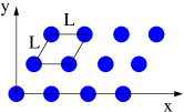

The lattice translation vectors are , . Hence, there are two independent reciprocal lattice vectors in the Brillouin zone (see Fig.1):
The points , , are connected by vectors , and are obtained from the by reflection. In order to simplify notation, we will measure energy in units of the bandwidth:
| (4) |
In the case of GaAs, assuming nm, which can be obtained experimentally with standard lithographic techniques, we have meV. Notice, however, this energy scale can be easily controlled by tuning (for nm, meV.
Unlike the case of graphene where the starting point is a tight-binding description Greview , our description starts from a nearly free electron description. We assume, for simplicity, a periodic potential with a single Fourier component:
| (5) |
where gives the strength of the potential. This potential has nonzero matrix elements only between states and with matrix elements given by . Diagonalization of the Hamiltonian,
| (6) |
gives the hole dispersion shown in Fig. 2(a) with the presence of two Dirac points with linear dispersion.
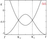
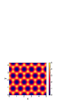
If the chemical potential is tuned at the Dirac point the average hole density is . The map of the charge density is shown in Fig. 2(b). At the average density is . Even when the potential is strong, namely , the dispersion, Fig. 2(a), is rather close to the result obtained by perturbation theory. The charge density plot, Fig. 2(b), is fully connected with empty spots at positions of the potential maximums. So, in clear contrast to graphene, at the system is much closer to the nearly free electron regime than to the tight-binding one.
Perturbative analysis of the system in the nearly free electron regime, at small , is straightforward Park09 . A hole state close to the Dirac point, , is described by degenerate perturbation theory as:
| (7) |
In the basis of states the Hamiltonian (6) is represented by matrices:
The eigen-energies of the U-matrix are . In order to project in the double degenerate subspace of we define Park09 :
| (14) |
Projecting the kinetic energy to this basis and shifting the zero energy level to one finds:
| (15) |
where , is the Fermi-Dirac velocity. Notice that the velocity is controlled by the lattice spacing. Hence, in the Pauli matrix (pseudo-spin) representation the effective low energy Hamiltonian reads:
| (16) |
One can perform the unitary transformation , where represents two subsequent rotations around x- and y-axes in the pseudo-spin space and transform the Hamiltonian to the conventional form of a 2D Dirac Hamiltonian: . However, in what follows we will use (16), as it is slightly more convenient for the study of the edge states.
The effective SOC arises due to the heavy-light hole mixing in the wave function ( Topological Insulating States in Laterally Patterned Ordinary Semiconductors). Certainly there are other SOC mechanisms such as Rashba, Dresselhaus, and even direct SOC with the modulating potential. However, all these mechanisms are relatively weak while the “ultrarelativistic” (see above) heavy-light hole mixing can give SOC comparable with the kinetic energy. The heavy-light hole mixing in the wave function ( Topological Insulating States in Laterally Patterned Ordinary Semiconductors) leads to the following SOC correction to the matrix element of the potential (5):
| (17) |
Here , and is the effective spin 1/2 introduced in ( Topological Insulating States in Laterally Patterned Ordinary Semiconductors). At long wavelengths the leading order contribution for the SOC is given by:
| (18) | |||||
which can be written as:
| (22) |
Projecting this matrix to the states and defined by (14) we get: . Thus, the final Hamiltonian, including (16), reads:
| (23) |
The Hamiltonian is written for the K Dirac cone. Under the parity reflection, , the kinetic energy ( Topological Insulating States in Laterally Patterned Ordinary Semiconductors) changes its sign while the SOC (18) is unchanged. Hence, at the Dirac point the effective Hamiltonian differs from (23) only by the replacement . After a unitary transformation the Hamiltonian (23) can be written in its conventional form Kane05 : leading to a SOC gap given by:
| (24) |
which shows that the SOC gap is a very strong function of the ratio.
SOC matrix elements (17) can be easily included in the exact diagonalization. Notice that eqs. ( Topological Insulating States in Laterally Patterned Ordinary Semiconductors) and (17) are derived assuming . Even at small this condition is violated for high momenta states included in the exact diagonalization. To avoid this problem we account (17) only for three lowest quantum states and set the SOC matrix element equal to zero for all higher states. This procedure gives the correct gap near the Dirac points. Notice that, for . The dispersion calculated numerically for this value of the SOC and is shown in Fig. 3a.
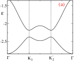
The calculated spin orbit gap is close to the analytical formula (24). By varying the transverse confinement width , see Eq.(24), one can continuously change the SOC gap and, hence, the electronic properties of devices made in these systems.
In order to study the presence of edge states we have to consider a sample with a confining potential at the edge. Having in mind simplicity, we consider an infinite edge potential. The mechanism of the edge state formation discussed here is qualitatively different from that in the graphene Greview because of the nature and strength of the potentials in the two cases: graphene is better described by the tight-binding model, while semiconductors are better described by the nearly free electron approximation. In graphene described by the tight binding approximation edge states exist even without the SOC (say, along the zig-zag direction), and the SOC only modifies the dispersion of the state Kane05 . On the other hand, in the nearly free electron approximation the SOC is crucial for the formation of the edge state.
Let us consider the effect of a laterally confining potential to the lattice potential (5). We assume:
| (27) |
The envelope wave function of the edge state at is given by:
| (30) |
Solving with Hamiltonian (23) one finds:
| (31) |
The corresponding full coordinate wave function reads:
| (32) |
where we have used Eqs. ( Topological Insulating States in Laterally Patterned Ordinary Semiconductors), (14) for and . The wave function must be zero at at the position of the confining wall. It is obvious that one cannot satisfy this condition at arbitrary . Fortunately, it is very easy to find the state if the wall position is chosen as: , where is integer. At the basis wave function is zero at any . Therefore, to have we need only to impose . Hence, using ( Topological Insulating States in Laterally Patterned Ordinary Semiconductors) we conclude that the edge state exists only at :
which is valid near the K Dirac point. We already pointed out that at the Dirac point the effective Hamiltonian differs from (23) only by the replacement . The edge solution ( Topological Insulating States in Laterally Patterned Ordinary Semiconductors) is transformed accordingly. Therefore, at K’ the edge state exists only at :
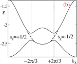
The dispersion of the edge states with is shown in Fig. 3(b). We found the edge states at a special position of the confining wall. An explicit calculation at a different wall position/shape is more involved since the calculation must include admixture of high momentum states to the wave function ( Topological Insulating States in Laterally Patterned Ordinary Semiconductors). However, a variation of the wall position/shape does not influence the edge states since they are topologically protected.
The edge states support the spin current at the edge of system in the regime of a TI. In Fig. 3 the energy is given in units of the bandwidth , Eq. (4), which depends on the period of the modulating potential. Present lithographic techniques can give the period nm in GaAs and nm in Si. According to Fig. 3 this results in the spin-orbital gap meV. By increasing the ratio the gap can be further boosted up by a factor . All in all the existing technology can produce a TI operating at temperature . Improvement of lithographic techniques down to scale nm will open way to tunable room temperature TI.
A disorder created by charged impurities, if strong, can destroy the miniband structure. There are two issues related to the disorder, (i) the hole mean free path, (ii) local fluctuations of the Fermi energy. In clean GaAs the electron mean free path is about 30m. For holes the mean free path is shorter, but still it is about 5m Chen12 , so on this side we are safe, the superlattice can be larger than 100100 sites. To estimate the inhomogeneity of Fermi energy we refer to Shubnikov de-Haas oscillations. For holes in clean GaAs the oscillations are observed down to magnetic field Tesla Chen12 . This corresponds to the cyclotron frequency meV and this is the upper limit for the Fermi energy inhomogeneity. So, we are safe here too.
In conclusion, we have shown that it is possible to create robust TI states in ordinary semiconductors with strong SOC by quantum confinement and superimposed potentials with hexagonal symmetry. We have shown that the SOC gaps can be as large as the heterostructure bandwidth and can be controlled by varying the confinement potential, the strength and scale of the superimposed potentials. These systems present amazing flexibility and can be tuned between completely different regimes such as the Dirac metal, TIs, and standard band insulators. Thus, they present an opportunity to study exotic physics in the framework of materials that have been the basis of the current semiconductor technology.
We thank A. R. Hamilton, T. Li, A. I. Milstein, and O. Klochan for discussions. OPS acknowledges ARC grant DP120101859. AHCN acknowledges DOE grant DE-FG02-08ER46512, ONR grant MURI N00014-09-1-1063, and the NRF-CRP award ”Novel 2D materials with tailored properties: beyond graphene” (R-144-000-295-281).
References
- (1) B. A. Bernevig, T. L. Hughes, S.-C. Zhang, Science 314, 1757, (2006).
- (2) M. Z. Hasan, and C.L. Kane, Rev. Mod. Phys. 82, 3045 (2010).
- (3) J. E. Moore, Nature 464, 194 (2010).
- (4) C. L. Kane and E. J. Mele, Phys. Rev. Lett. 95, 226801 (2005).
- (5) A. H. Castro Neto et al., Rev. Mod. Phys. 81, 109 (2009).
- (6) A. H. Castro Neto and F. Guinea, Phys. Rev. Lett. 103, 026804 (2009).
- (7) M. Konig et al., Science 318, 766 (2007).
- (8) L. Fu, and C.L. Kane, Phys. Rev. B 76, 045302 (2007).
- (9) Hsin Lin et al., Nat. Mat. 9, 546 (2010).
- (10) C. L. Kane and J. E. Moore, Physics World 24, 32 (2011).
- (11) C. Liu et al., Rev. Lett. 100, 236601 (2008).
- (12) I. Knez, R.-R. Du, and G. Sullivan, arXiv:1105.0137.
- (13) See, for instance, R. Winkler, Spin-Orbit Coupling Effects in Two-Dimensional Electron and Hole Systems (Springer-Verlag, Berlin, 2003).
- (14) A. H. Castro Neto, F. Guinea, and N. M. R. Peres, Phys. Rev. B 73, 205408 (2006).
- (15) J. M. Luttinger and W. Kohn, Phys. Rev. 97, 869 (1955).
- (16) I. Vurgaftman, J. R. Meyer, and L. R. Ram-Mohan, J. Appl. Phys. 89, 5815 (2001).
- (17) C.-H Park and S. G. Louie, Nano Letters, 9, 1793 (2009).
- (18) M. Gibertini et al, Phys. Rev. B 79, 241406(R) (2009).
- (19) A. Singha et al, Science 332, 1176 (2011).
- (20) J. C. H. Chen et al, Appl. Phys. Lett. 100, 052101 (2012).