Optical signatures of the tunable band gap and valley-spin coupling in silicene
Abstract
We investigate the optical response of the silicene and similar materials, such as germanene, in the presence of an electrically tunable band gap for variable doping. The interplay of spin orbit coupling, due to the buckled structure of these materials, and a perpendicular electric field gives rise to a rich variety of phases: a topological or quantum spin Hall insulator, a valley-spin-polarized metal and a band insulator. We show that the dynamical conductivity should reveal signatures of these different phases which would allow for their identification along with the determination of parameters such as the spin orbit energy gap. We find an interesting feature where the electric field tuning of the band gap might be used to switch on and off the Drude intraband response. Furthermore, in the presence of spin-valley coupling, the response to circularly polarized light as a function of frequency and electric field tuning of the band gap is examined. Using right- and left-handed circular polarization it is possible to select a particular combination of spin and valley index. The frequency for this effect can be varied by tuning the band gap.
pacs:
78.67.Wj,78.67.-n,75.70.Tj,73.22.PrI Introduction
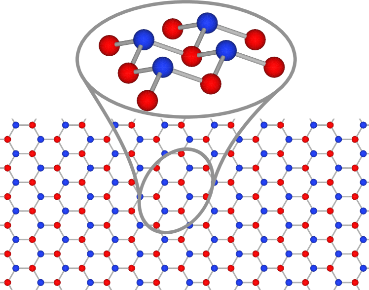
The experimental realization of two-dimensional crystals has sparked a flurry of research activity. The prototypical example was the isolation of graphene,Novoselov et al. (2004, 2005) a single layer of carbon atoms, with its remarkable physics due to the Dirac fermionic nature of its charge carriers. Much research has ensuedNeto et al. (2009); Abergel et al. (2010); Das Sarma et al. (2011); Kotov et al. (2012) and part of the focus is on the potential to manipulate the physics of these charge carriers to benefit technological applications. In graphene the charge carriers show a linear dispersion near the Fermi levelWallace (1947) with chiral properties attributed to the topological aspect of two sublattices in a hexagonal crystal lattice. This leads to a mapping of the low energy nearest neighbor tight-binding Hamiltonian on to a Dirac equation for massless fermions which exist at and in the hexagonal Brillouin zone.Semenoff (1984) The conical disperison at these points are referred to as valleys and many properties in graphene are spin degenerate and valley degenerate. As the spin-orbit interaction in graphene is quite smallKonschuh et al. (2010) and therefore neglected, interesting effects, such as inducing spin-valley coupling discussed here, will not be evident. This is unfortunate as much interesting physics and potential for spin manipulation will not be manifest in graphene. Given some of the limitations of graphene in this regard, attention has turned to other 2D crystals which have graphene-like features but stronger spin-orbit coupling. One such material is silicene, a monolayer of silicon atoms arranged in a honeycomb lattice, as in graphene. As silicon is already used in electronics and a large silicon manufacturing industry is in place, it bears closer inspection. Silicene has only recently been made in ribbonsAufray et al. (2010); Padova et al. (2010); Lalmi et al. (2010) and an experimental literature has yet to be developed. However, numerical calculations have shown that it should be possible to make silicene suitable for transfer to a substrate where it might be gated.Cahangirov et al. (2009); Drummond et al. (2012) As silicon has a stronger spin-orbit coupling than graphene, it will exhibit more clearly an energy gap in the band structure. It has been argued that in this circumstance, the Dirac nature of the fermions makes a topological insulator (TI). One of the interesting predictions for silicene involves that of inducing a tunable band gapDrummond et al. (2012) which would give rise to a transition between a topological insulator and a band insulator (BI).Drummond et al. (2012); Ezawa (2012a) This comes about due to the fact that in silicene, the size and distance between silicon atoms leads to a buckling of the structure where one sublattice is shifted upwards out of the 2D plane relative to the other (see Fig. 1). This means that an applied electric field perpendicular to this plane changes the sublattice potential and produces a tuning of the band gap in the dispersion.Drummond et al. (2012) Furthermore, the bands are spin-split in a valley-dependent way allowing for an examination of spin-valley coupling.Ezawa (2012b) Other examples of systems discussed in the literature which are predicted to show spin-valley coupling are MoS2 and other group-VI dichalcogenidesXiao et al. (2012); Cao et al. (2012) and a monolayer of germanium (germanene)Liu et al. (2011). Currently, MoS2 has been the subject of several experimental investigations, for example Ref. Mak et al. (2010, 2012); Zeng et al. (2012); Cao et al. (2012); Sallen et al. (2012), while silicene is still in its infancy and germanene has yet to be synthesized. Nonetheless, we will use the examples of silicene and germanene as a models to examine issues associated with spin-valley coupling and optical signatures of a TI to BI transition.
In this work, we study the finite frequency conductivity of a material such as silicene which can be induced to have spin-valley coupling and a tunable band gap. We find that there are characteristics in the far infrared or THz conductivity which would allow for the differentiation of the TI versus the BI. With tuning of the band gap, these features could be used to identify the critical point of transition and allow for an experimental determination of the strength of spin orbit coupling in these systems. We also consider the effect of finite doping and circularly polarized light as possible probes of spin-valley coupling. Previous issues associated with circular dichroism are revisited in view of performing broadband spectroscopy.
Our paper is organized in the following manner. In Section II, we briefly describe the basic Hamiltonian and approximations used in this work and outline the nature of our calculation of finite frequency conductivity. Following this, in Section III, we feature our results for the absorptive part of the longitudinal optical conductivity and provide a discussion of the physics. In Section IV, we discuss the case of circularly polarized light which illustrates the potential for spin-valley polarization and its the tuning by electric field. Our conclusions are summarized in Section V.
II Theoretical Background
Recently, there have been theoretical works which have calculated the band structure of siliceneLiu et al. (2011); Drummond et al. (2012) using density functional theory including effects due to spin-orbit coupling (SOC) and a perpendicular electric field. The spin-orbit band gap has been found to be about 1.5 meV and this can be increased to 2.9 meV under strain.Liu et al. (2011) This latter study has also predicted a SOC band gap of 23.9 meV for 2D germanium or germanene. In the work of Drummond et alDrummond et al. (2012), a SOC gap of 1.4-1.5 meV is also found for silicene and with a perpendicular electric field, the resulting gap may be tuned up to tens of meV before other transformations occur. This work along with that of EzawaEzawa (2012a, c, b) suggest that much of this behavior may be captured by a simple low energy Hamiltonian written about the K point labeled :
| (1) |
where is the valley label for the two K-points, which were previously referred to as and . The first term is the Hamiltonian for Dirac electrons with velocity (we take ), the second term is the Kane-Mele SOC term with SOC gap and the last term is associated with the perpendicular electric field which, when applied across the buckled structure, gives rise to an A-B sublattice asymmetry with on-site potential where is the perpendicular distance between the two sublattice planes. The matrices and are the Pauli matrices. The former act on the pseudospin space associated with the A and B sublattices and the latter are for real spin with , the z-component. In the papers by Ezawa, a Rashba SOC is included in addition to the intrinsic SOC used here. As the Rashba SOC is an order of 10 smaller in magnitude, we neglect it. Therefore, the full 8x8 matrix spanning both points is block diagonal in 2x2 matrices labeled by valley index for and and spin index for spin up and spin down, respectively:
| (2) |
The eigenvalues are evaluated from the Hamiltonian above to be:
| (3) |
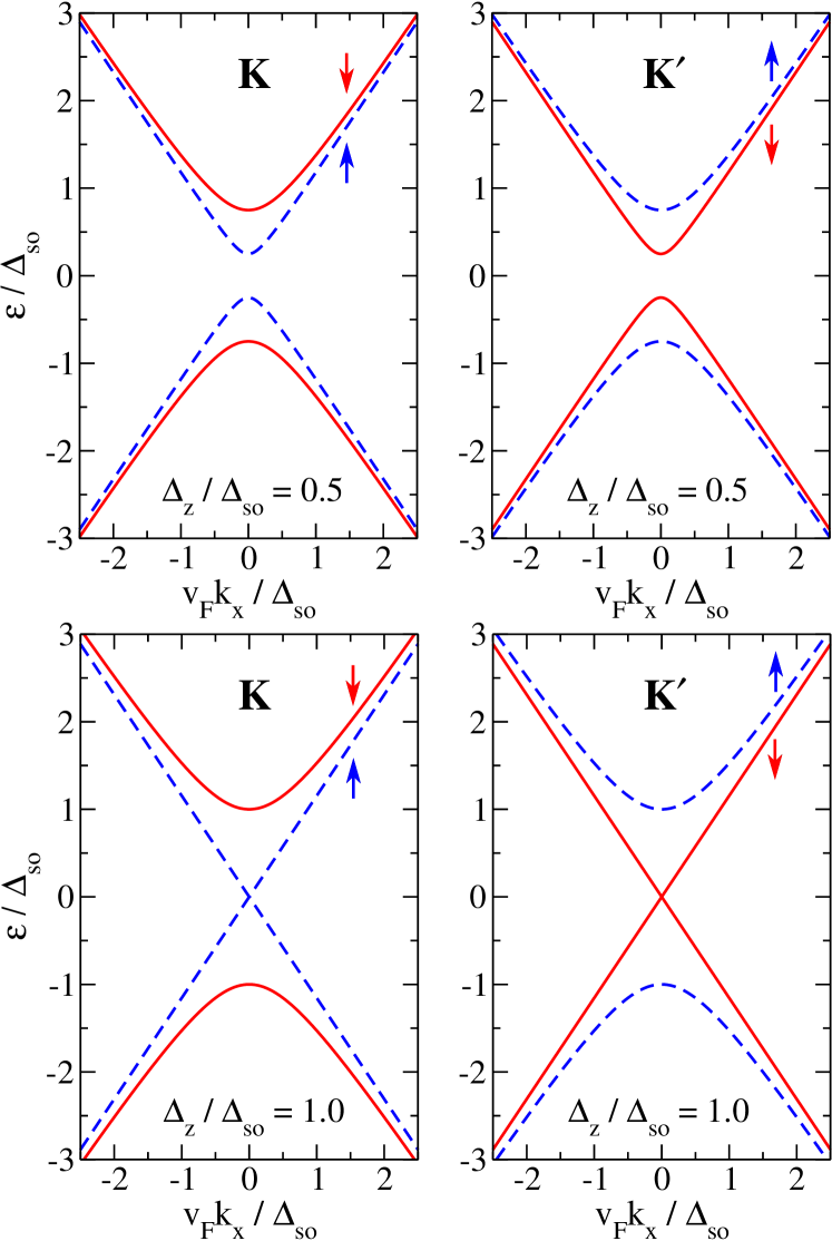
These are plotted in Fig. 2 for a value of where the bands are spin-split, reversed at the other point, and represent a topological insulator. Also shown is the case where . At this critical point, the gap of one of the spin-split bands closes to give a Dirac point while at the other point it is gapped and it is the other spin band which has no gap. This has been termed a valley-spin-polarized metal (VSPM).Ezawa (2012c) For , the spectrum becomes fully gapped again but the system is a band insulator albeit with unusual chiral properties.Drummond et al. (2012) In the case of , the bands are spin degenerate with a single band gap of . In Fig. 3, we show the total density of electronic states for the bands shown in Fig. 2.
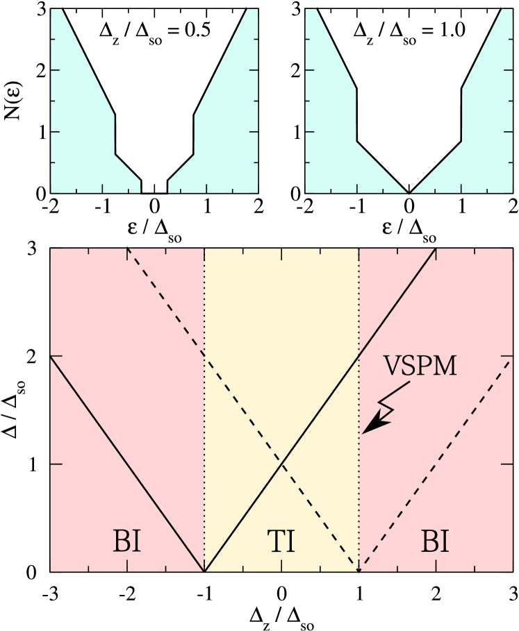
The density of states reflects the two gaps that open in the system depending on the strength of . At the critical value where , which is the VSPM state, the low energy density of states is linear out of zero energy and jumps at a value equal to the sum of to further linear behavior with double the slope (upper righthand frame of Fig. 3). This jump reflects the spin-split bands. For finite , a low energy gap appears at a value of the difference of these two energies and a jump at higher energy remains (upper lefthand frame). If , there is only the spin-orbit gap and the spin degeneracy in this case gives just the one gap edge with no further jumps in the density of states. This behavior is embodied in the following formula for the density of states:
| (4) |
where
| (5) |
and , with indexing the spin up/down bands at the point. A plot of the energy gaps for the spin-resolved bands are shown in the lower frame of Fig. 3, where the solid curve follows the notation of Fig. 2 and indicates the gap for the spin down band and the dashed line is for the spin up band at . The solid and dashed lines would reverse in the plot for the point, as seen in Fig. 2. The region of electric field that gives has been shown to pertain to a TI of the Kane-Mele type (or a quantum Hall spin insulator) and for , the system is a BI. The critical point at which is the VSPM state discussed previously. It is clear from this figure that in the BI state, both gap edges in the DOS will increase with the magnitude of the perpendicular electric field, whereas in the TI case, the higher one will increase with electric field while the lower one decreases, which would be a method of differentiating between the density of states of the BI versus the TI.
Such considerations also will apply to the dynamical conductivity which we evaluate by the usual Kubo formalism.Nicol and Carbotte (2008); Carbotte et al. (2010); Tabert and Nicol (2012) The zero temperature, absorptive part of the conductivity at photon frequency is given from an evaluation of
| (6) |
where is the chemical potential, , with referring to spatial coordinates in 2D, and is the spectral function of the Green’s function found from through the relation
| (7) |
Using Eq. (6) and the appropriate operator, we obtain the expression for the real part of the zero temperature longitudinal conductivity
| (8) |
where the response associated with a particular spin in a particular valley is given as
| Re | ||||
| (9) |
with
| (10) |
| (11) |
and is given by Eq. (3). From this we are able to obtain analytically, the real part of the longitudinal conductivity and its Kramers-Kronig-related imaginary part. These are given as
| (12) | ||||
| (13) |
where , , and . Likewise, the imaginary part of the zero temperature transverse or dynamical Hall conductivity for a given spin and valley is given by
| Im | ||||
| (14) |
where and are given by Eqs. (10) and (11), respectively. This can be solved analytically for the imaginary part and the Kramers-Kronig-related real part. These are
| (15) | ||||
| (16) |
Similar analytic forms have been found in other works for other systems.Gusynin et al. (2006); Tse and MacDonald (2010) With these formulas in hand, we can now discuss the longitudinal conductivity and the conductivity for circular polarization associated with the different valley and spin degrees of freedom. Our aim is to identify signatures of of the VSPM state and the TI to BI transition.
III Longitudinal optical response
In this section, we discuss the results for the real part of the frequency-dependent longitudinal conductivity. For our calculations shown in the figures, we have chosen to evaluate Eqs. (8) and (9), where we have replaced the delta functions in the spectral functions with Lorentzians according to with , a broadening parameter taken to be . (Note that the Kramers-Kronig related piece of the delta function in will have to be replaced with that for the Lorentzian form.)Tabert and Nicol (2012) This mimics impurity scattering in the system, with the transport scattering rate . This is done to provide more realistic looking curves, however, the analytical formulas above work very well if the delta function is replaced with a Lorentzian with halfwidth associated with the transport impurity scattering rate, instead of which is the quasiparticle scattering rate in the spectral function.Nicol and Carbotte (2008); Tabert and Nicol (2012)
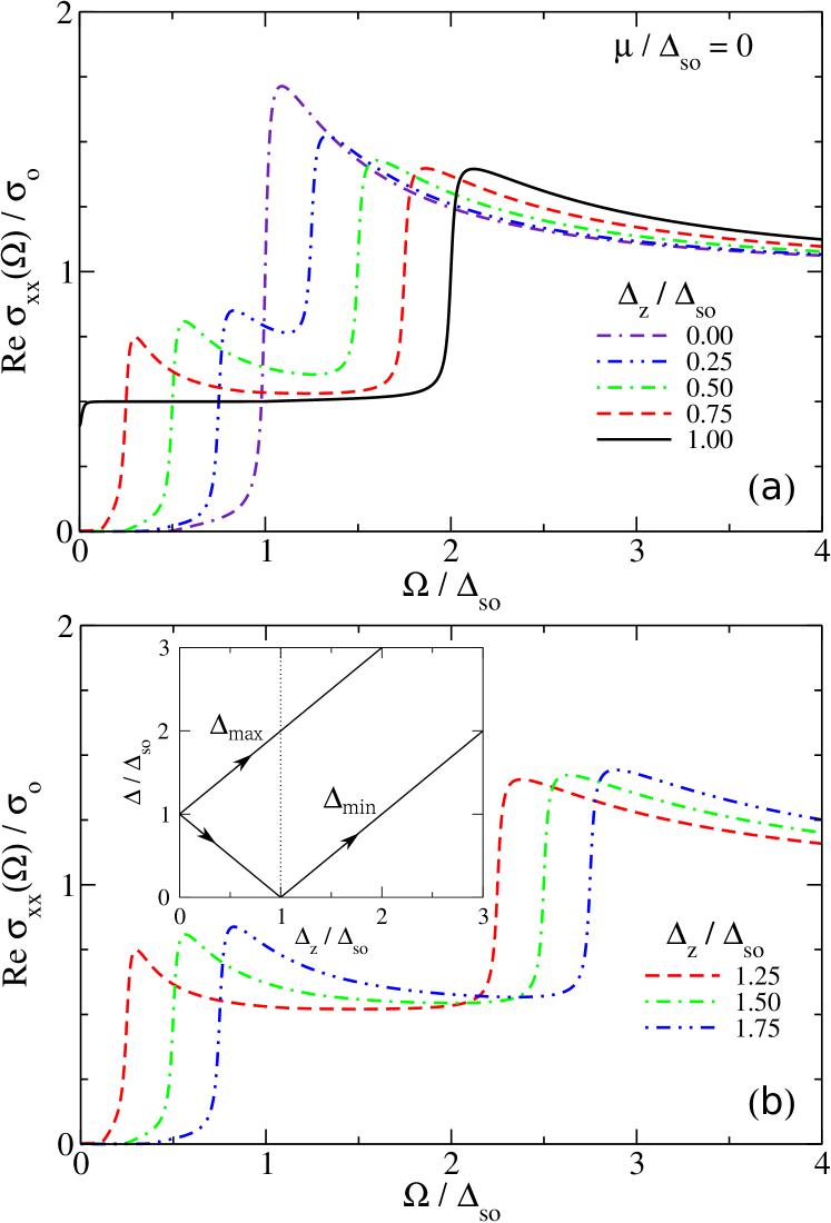
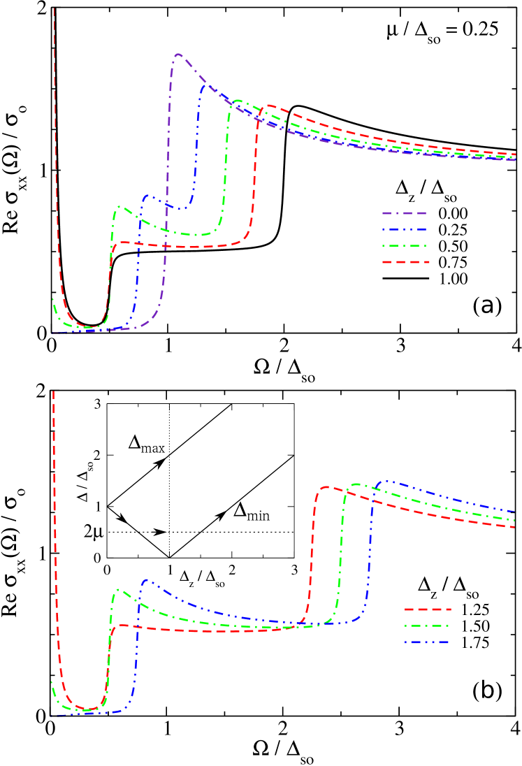
For the case of charge neutrality, where , we have results shown in Fig 4. The conductivity is entirely based on interband transitions. For , we have only spin orbit coupling, the bands are degenerate in spin with a single gap, and there is one absorption edge at which shows a peak before decaying to the universal background expected for a monolayer graphene-like system. With finite (the TI regime), two edges appear due to the spin-split bands giving rise to two gaps as discussed in Fig. 3. (Note that transitions can only occur between bands with the same spin index.) The absorption edges track the gaps shown in Fig. 3 bottom frame (and reproduced here in the inset for positive ) such that the edges move oppositely in frequency - a signature feature of the TI region. At the VSPM point (), the VSPM gives the famous Dirac massless fermion conductivity, which is flat, but the amplitude is only one half that of which is different from the case of graphene where it is . At the energy scale of there is now an absorption edge leading to a peak structure, as before, with the onset of the interband transitions between the gapped bands. This curve is a signature for the VSPM state. For the region for the BI (), two interband edges occur, the peaks of which both move outward according to the sum and difference of and , but with a constant separation in energy of . The behavior of the absorption edge peaks from the TI to BI regimes tracks the arrows of the inset, i.e., as increases from zero, the two peaks move oppositely in the TI region and then both move to higher frequency in the BI region. The plots shown here are for the total longitudinal conductivity. For the longitudinal conductivity about one point, the same frequency dependence remains and one merely has half the magnitude, although the lower frequency segment would represent the response of charges with one particular spin orientation and the larger energies are associated with the superposition of the response of both spin orientations. It is clear that from the frequency dependence, one could identify the spin orbit energy gap value by tracking the behavior with perpendicular electric field. The extrapolation of the minimum gap to zero as a function of identifies the critical electric field that produces the VSPM, and the identification of the two regimes, TI versus BI, is found by looking for co-moving or counter-moving peaks.
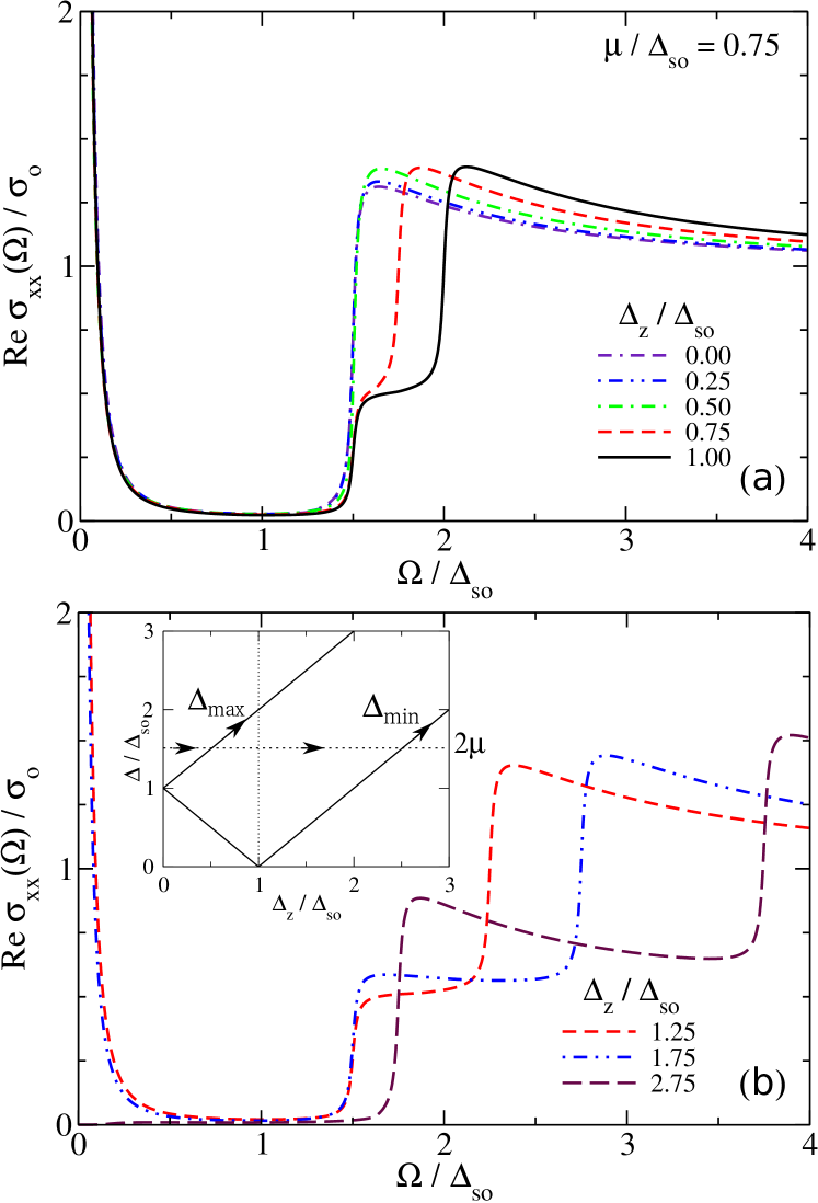
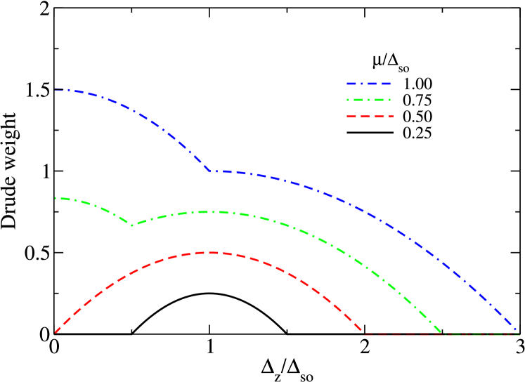
Of course, some things change in the doped case. Primarily, the lowest energy for absorption at a given electric field strength is set by or , whichever is greater. This is most easily illustrated with Figs. 5 and 6 where twice the chemical potential is taken to be finite but less than in the former case and greater than in the latter one. The Pauli-blocking cutoff is well-known in graphene where vertical transitions from an occupied state to an unoccupied state cannot occur in the band structure for photon absorption frequency . In Figs. 5 and 6, we see that the same pattern from the case is occurring with the exception that there is a lower energy cutoff based on the inset figures illustrating the progression of the energies of the absorption edges with varying (following the arrows in the inset). For , and the lower absorption edge decreases until where it remains stationary until it starts to increase in frequency at . Note that an intraband Drude conductivity also appears during the range of where the lowest absorption edge remains at , i.e. or . At this point the chemical potential is in the band and consequently intraband absorption processes can occur. This leads to an interesting observation that varying electric field at finite doping could provide a mechanism to switch on and off the Drude response at low frequency due to the Fermi level falling outside and inside the band gap as tuned by . This is illustrated in Fig. 7 where we plot the Drude weight (the amount of spectral weight under the delta function of for ). Examining the black curve with , is less than the minimum gap for at which point only interband transitions can occur. For increased , however, the minimum gap decreases and the Fermi level is in the band and an intraband Drude absorption occurs. The maximum occurs at the point at which the VSPM is reached and then the Drude weight decreases as the minimum gap once again increases with in the BI regime. When the electric field strength becomes strong enough to increase the minimum gap value further, the Fermi level will once again fall in the gap rather than in the spin split band and the Drude intraband absorption will disappear (as it does here at ). Thus, for , the Drude weight appears within the region where the minimum gap drops below (as shown in the inset of Fig. 5). For , the Drude weight is always present until the minimum gap overcomes (refer to the inset of Fig. 6). The kink in the curve occurs when is equal to the maximum gap. Moreover, if the Fermi level is between the spin split bands, the Drude weight will show an increase in the TI region as is increased and then decrease again as the system is tuned into the BI region.
IV Circular polarization
Circularly polarized light has been suggested as a mechanism for seeing the valley-spin coupling in siliceneEzawa (2012b) and in group VI-dichalcogenidesXiao et al. (2012); Cao et al. (2012). In light of this suggestion, we discuss the full frequency dependence of the optical response of silicene to circularly polarized light. Our discussion is somewhat different from that of other referencesXiao et al. (2012); Cao et al. (2012); Ezawa (2012b) where the focus has been on the matrix elements evaluated in momentum space for specific frequencies. Here we look at the broadband response. For finite frequency optical response in the circular polarization basis, the conductivity is given as for righthanded () and lefthanded () circular polarization.Pound et al. (2012) The real part of this function provides the absorptive part of the optical response:
| (17) |
which can be obtained from our previous formulas. This form refers to the total absorptive response to circularly polarized light which is written in terms of the absorptive parts of the longitudinal and transverse conductivities which have been summed over valley and spin indices. It will facilitate our discussion to show the components which are summed over spin but plotted separately for each valley index, ie.,
| (18) |
and we decompose further to show the individual components based on valley and spin (the quantity in the square brackets of Eq. (18)).
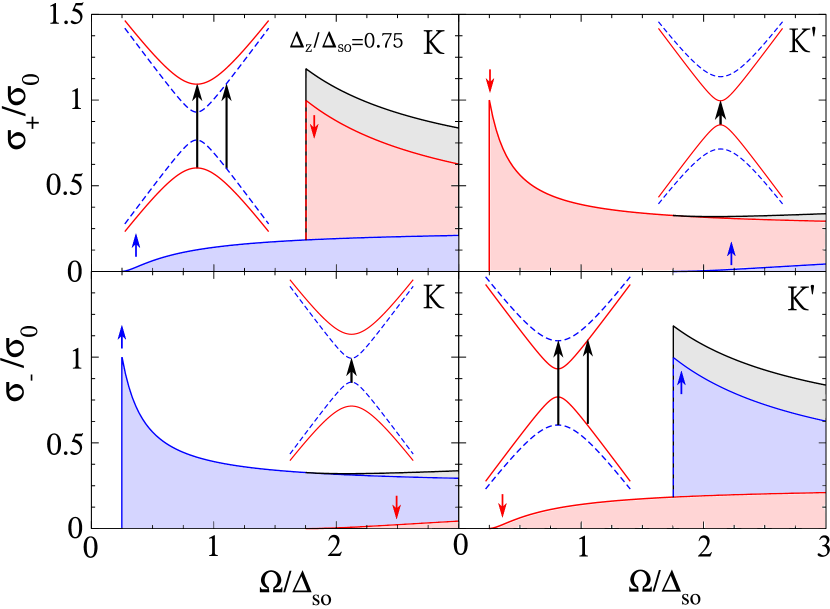
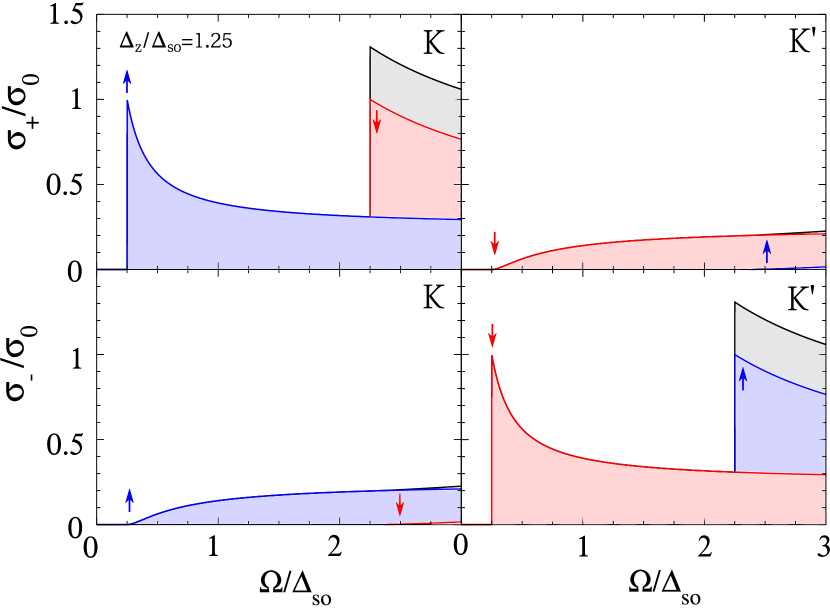
To begin with, we show in Figs. 8 and 9 plots to illustrate the essence of our results. We have chosen for these plots to use the analytical formulas in order to simplify and sharpen the structure and to allow us to make comparison with other figures later on for a discussion about the effect of broadening which we have not had up till now. In Fig. 8, we show the case of which is the TI regime and in Fig. 9 we take which is in the BI regime. In the four frames, we plot the response to circularly polarized light for each combination of and point and polarization. The blue area indicates the spin up component and the red region, the spin down (as indicated by the arrows).
Considering first Fig. 8, it is quite apparent that with positive polarization and a frequency associated with the minimum gap , the optical response is dominated by charge carriers with down spins residing in the valley, whereas, for negative polarization, at the same energy, the response is due to charge carriers with up spins in the valley. Hence, circularly polarized light provides a means to populate valley-specific carriers with a particular spin orientation. The frequency required is that corresponding to the minimum gap in the band structure and indicated by an arrow on the band structure insets of the upper right frame and lower left frame of Fig. 8. Such an idea has been discussed previously for silicene by EzawaEzawa (2012b) and by others for the dichalcogenides.Xiao et al. (2012); Cao et al. (2012) It was also argued in those works that using a photon energy associated with the maximum gap would connect the two outer bands, thus allowing for absorption at that frequency which would be associated with the other spin orientation for each valley. That is, for shown here, the dominate response is to see the down spin charge carriers in the valley and the up spin ones for the point. However, as is clear from these four frames, the circularly polarized response at will not be purely of one spin orientation, nor when the response of the two valleys are added for a particular polarization, will it be the response of just one valley at that frequency. As shown in the inset band structure pictures for the upper left and lower right plots, even though will connect the two outer bands at to give a peak in the absorption, it will also connect states from the inner two bands at finite , and the total absorption is the sum of the two (the black curve). Thus, the lowest frequency is robust for producing valley-spin polarized charge carriers but the upper frequencies will be contaminated and not result in a pure spin-valley polarized response. So we conclude that using photons with energy will produce (,) and (,) in this case, given negative and positive circular polarization, respectively. The question might then be asked as to whether one could produce the other combinations in an uncontaminated way. If one returns to the bottom frame of Fig. 3, it can be noted that if changes sign, this reverses the spin labels on the bands at the valley (indicated by the dashed and solid lines) and likewise at the valley and so, at least from a theoretical point of view, (,) and (,) could also be excited at with oppositely polarized light if one could reverse the electric field without changing anything else.
In the BI regime, shown in Fig. 9, the essential difference is that the lower band spin response is switched between the two polarizations for a fixed point and so a double peak structure appears in the positive polarization response of the valley and very little occurs in the negative polarization at the same point (with the results reversed at the valley). Such behavior was also noted by Ezawa and is due to band inversion in the BI relative to the TI.Ezawa (2012b) Thus, one finds that once again, the lowest energy defined as as before, will reflect a single spin state, but now associated with the opposite polarization from the case of the TI. For the total response to polarized light as a function of frequency, in the case of a BI, probes mainly the point and , the one, and the two peaks in the frequency dependence are associated with different spin orientation. Whereas for the TI, excites primarily down spins and , up spins, and it is two peaks in the frequency dependence that resolve the valley-dependence.
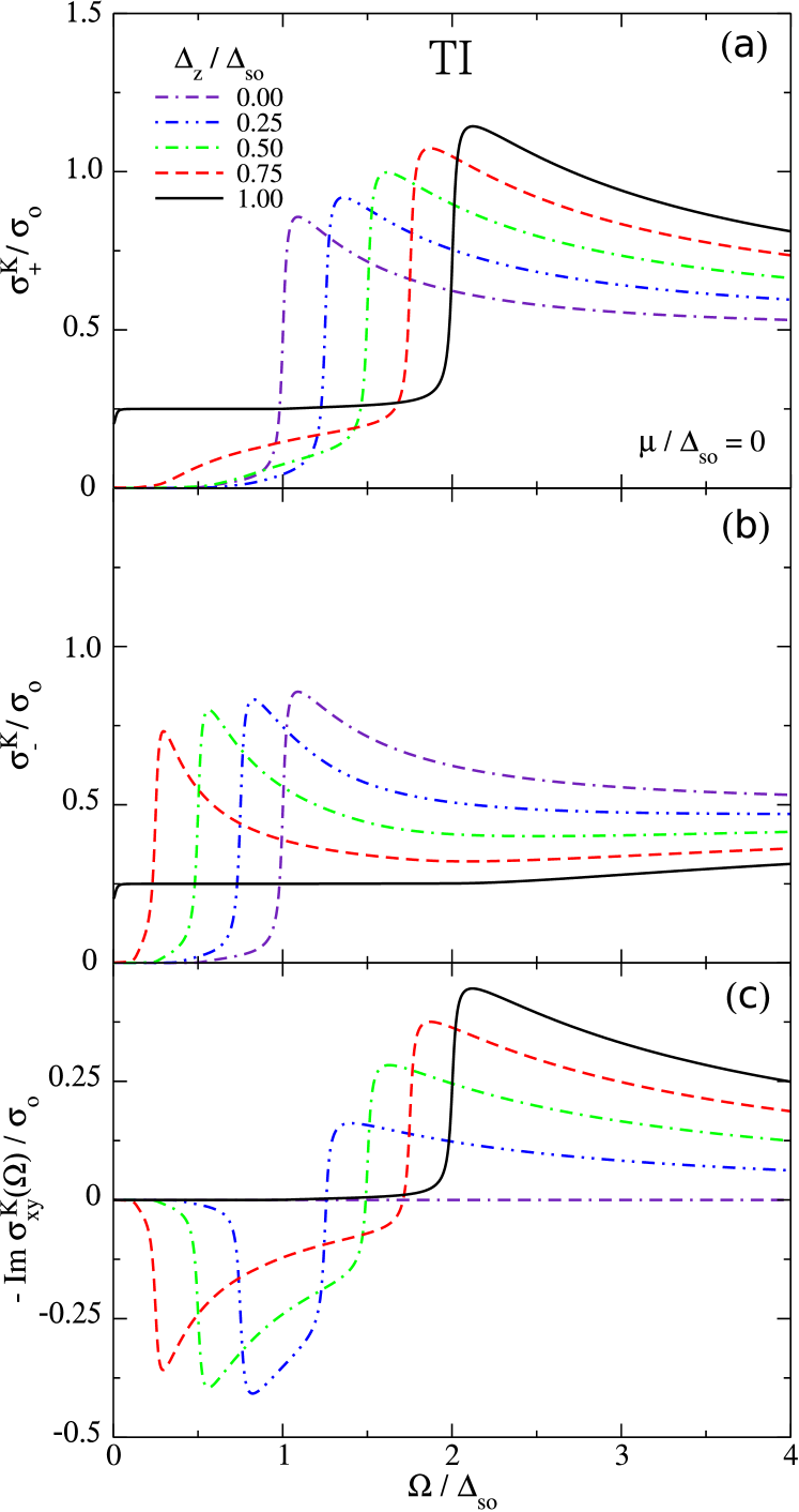
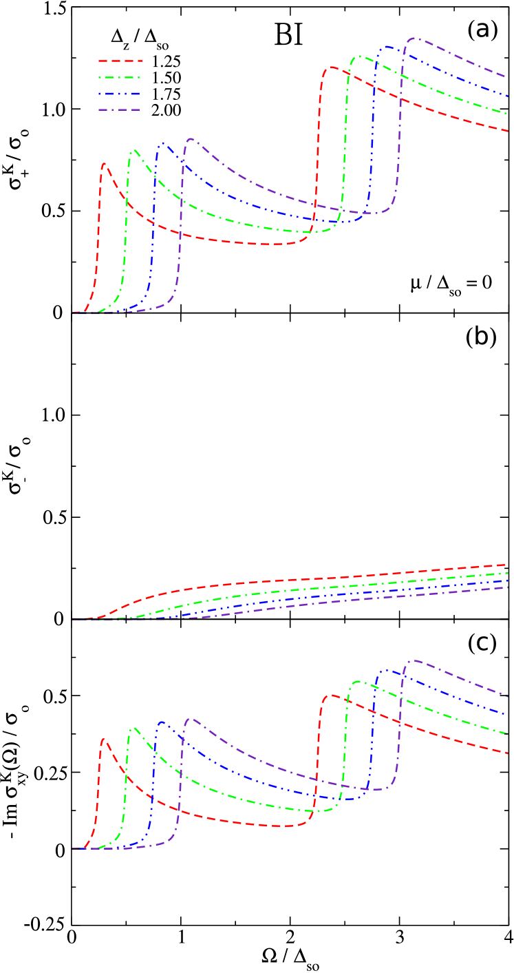
Now we comment on the variation of these curves with . Given that the valley is always the same but reversed with respect to the valley, as we have discussed, we will only show the valley results in the following. In Figs. 10 and 11, we show the response for for circularly polarized light , , and the imaginary part of the Hall conductivity as we vary . Note that and is therefore a measure of circular dichroism. These figures are only for the one point. For the point, the curves are the same except reversed in polarization label and spin orientation information (see Figs. 8 and 9) and reversed in sign in the case of . The cases for the TI and VSPM are shown in Fig. 10 and the BI, in Fig. 11. The first thing to note is that compared to Figs. 8 and 9, the peaks are suppressed and broadened due the impurity scattering included in these curves, Note, for instance, that the lowest peaks in Fig. 10(b) are not at a value of 1 as seen in Fig. 8, but are reduced by a significant amount. This is due to the broadening and the reduction is stronger when the energy scale of the peak edge is smaller and therefore closer to the energy scale of the broadening parameter. As a result, these curves present a more realistic sequence in behavior with variation with . While we do not identify the separate spin components as in Figs. 8 and 9, one can see that the overall envelope of the curves in Figs. 8 and 9 (i.e., the sum of blue and red to give the black curve) is the same here and so one may use Figs. 8 and 9 as a guide to identify the spin orientations associated with the peak structures in Figs. 10 and 11. Once again for the TI case, the pattern remains that the peak seen in the lefthanded polarization is primarily due to up spins and that seen in the righthanded polarization is due to down spins superimposed on a background of absorption due to transitions between the up-spin bands. In the BI case, there is only a response in one of the polarizations (righthanded in this case), however the lower peak is spin-selected for up spins while the upper absorption edge is again an admixture of the response of two spin species, dominated by down spins. The lefthanded polarization shows virtually no response by comparison. The interesting feature of these curves is that the absorption edges move with electric field tuning as seen before in the case of the longitudinal conductivity. As a result, the frequency at which the light can excite carriers with a certain spin orientation in a particular valley can be tuned (i.e., the discussed before depends on ). Following the discussion in our previous section for the longitudinal conductivity, there will be movement of these peaks in frequency according to the minimum and maximum gap and they will be suppressed by a cutoff when is greater than the gap energy. Such behavior will allow for additional flexibility in tuning the frequency at which valley-spin polarized carriers are excited, and the curves shown here illustrate that the response may not always be 100%.
If one takes the difference between these two polarizations, i.e., to obtain , a change in sign is seen for the TI case at the energy of but not for the case of the BI, where it is merely additive. As we have seen, is the point where the dominant response transitions from one spin species to the other. Of course, due to the sign change from one valley to another in , the total response for is identically zero. We note at this point that the total , summed over valleys and spins, will be the same function as , but that the character of the absorptive response for circular polarization of light will be associated uniquely with a particular spin and valley index, particularly at the lowest absorption edge. Consequently, keeping this in mind, we do not show results for finite doping but use the longitudinal case for reference. The primary effect of finite doping where is to eliminate absorption at lower frequencies and induce a Drude response. However, the Drude response will not show spin-valley polarization under circularly polarized light.
Finally we discuss the VSPM. This is shown as the solid black curve in Fig. 10 for . The low frequency response of the Dirac-type dispersion is the flat background seen in (a) and (b) associated with up spins of the valley. The magnitude is in both cases. The result at is reversed such the flat background is due to down spins. As the two points must be added for the total , there is an equal admixture of spin up and spin down, regardless of the sign of circular polarization and so one would need a mechanismXiao et al. (2007); Yao et al. (2008) that would allow for sampling one valley only in order to see a single spin state associated with the linear bands. The only variation in response occurs at when the upper band due to the opposite spin species enters and then a peak appears in for down spins, superimposed on the flat background due to up spins. In at the one valley, there is only one peak as opposed to two for the BI or two with opposite sign for the TI with finite . As a final comment, we wish to note that for , the bands are not spin-split and as a result, there is no circular dichroism or valley-spin polarization.
It is important to reiterate that while we show valley-separated curves here, the total response of a particular polarization is the sum over the two valleys and hence, the result will simply look like the curves for seen in previous figures. The point here is that the lowest peak in those curves is actually associated with a particular spin and valley when looked at with circular polarization. With other mechanismsXiao et al. (2007); Yao et al. (2008) for separating out the valleys, the extra information shown here may be accessible.
V Summary
We have calculated the optical response of silicene and related materials, such as germanene, which are predicted to exhibit a tunable band gap due to an applied perpendicular electric field. Due to the interplay of spin orbit coupling and the electric field strength, the bands display spin-valley coupling. Tuning of , allows for rich behavior varying from a topological insulator to a band insulator with a valley spin-polarized metal at a critical value in between. We find that in the longitudinal dynamic conductivity, two peaks marking interband absorption edges will shift oppositely in frequency with increasing in the TI phase and in the BI phase, will move in tandem to higher frequency, separated by . The VSPM exhibits a flat graphene-like conductivity at lower frequencies changing to a single peak at due to a second spin-split band with a band gap of . We suggest that seeing some of these features or tracking the variation of the peaks with should allow for the identification of these phases and the determination of parameters such as and the critical electric field that produces the VSPM. We have also noted the tunable band gap of this system could allow for a switching on and off of the Drude or DC response which may be of interest for technological applications. With predicted to be about 1.5meV in silicene and 25meV in germanene, this spectroscopy should fall in the realm of the THz to far-infrared. These spectroscopic ranges have successfully probed the dynamic conductivity of a variety of materials, for example, the first observation of the far-infrared conductivity of graphene,Li et al. (2008) and the 1.4 meV energy gap in superconducting Pb measured most recently in the THz range.Mori et al. (2008) Consequently, this should be quite feasible once appropriate samples are developed.
Another interesting aspect of this study is the consequences for circularly polarized light. We have shown that using circularly polarized light will resolve the spin and valley degrees of freedom. For instance in the TI with a perpendicular electric field yielding spin-split bands, the spin up charge carriers at the valley can be resolved by lefthanded circularly polarized light and the spin down ones at with righthanded polarization. Moreover, righthanded/lefthanded polarization probes primarily spin up/down carriers as a function of frequency. Tuning the electric field into the BI phase causes a band inversion such that the -valley spin-up carriers are now resolved with righthanded polarization and spin-down ones at with the lefthanded case, and circularly polarized light resolves primarily one valley as a function of frequency. A reversal of the perpendicular field direction could also reverse the spin-valley polarization for these two cases. The range of frequency for obtaining a single spin orientation in the response is largely restricted to the region about lowest frequency peak in the interband absorption. Doping above the minimum gap edge will simply shift the spectral weight to an intraband or Drude component which will not be spin-valley resolved. At present, no experiments of this type exist on silicene, but a demonstration of tuning the band gap from TI to BI in such systems would be of great interest. Other materials, namely the group VI dichalcogenides, are in the BI limit and predictions for the dynamic conductivity are being examined for MoS2 by others.Li and Carbotte (2012) Given the potential for further developments with 2D crystals, we anticipate that the optical properties and band gap tuning will play an important role in the investigation of new materials and the development of new technologies.
Acknowledgements.
We thank Jules Carbotte for discussions. This research was supported by the Natural Sciences and Engineering Research Council of Canada.References
- Novoselov et al. (2004) K. S. Novoselov, A. K. Geim, S. V. Morozov, D. Jiang, Y. Zhang, S. V. Dubonos, I. V. Grigorieva, and A. A. Firsov, Science 306, 666 (2004).
- Novoselov et al. (2005) K. S. Novoselov, D. Jiang, F. Schedin, T. J. Booth, V. V. Khotkevich, S. V. Morozov, and A. K. Geim, Proc. Natl Acad. Sci. USA. 102, 10451 (2005).
- Neto et al. (2009) A. H. C. Neto, F. Guinea, N. M. R. Peres, K. S. Novoselov, and A. K. Geim, Rev. Mod. Phys. 81, 109 (2009).
- Abergel et al. (2010) D. S. L. Abergel, V. Apalkov, J. Berashevich, K. Ziegler, and T. Chakraborty, Adv. in Phys. 59, 261 (2010).
- Das Sarma et al. (2011) S. Das Sarma, S. Adam, E. H. Hwang, and E. Rossi, Rev. Mod. Phys. 83, 407 (2011).
- Kotov et al. (2012) V. N. Kotov, B. Uchoa, V. M. Pereira, F. Guinea, and A. H. Castro Neto, Rev. Mod. Phys. 84, 1067 (2012).
- Wallace (1947) P. R. Wallace, Phys. Rev. 71, 622 (1947).
- Semenoff (1984) G. W. Semenoff, Phys. Rev. Lett. 53, 2449 (1984).
- Konschuh et al. (2010) S. Konschuh, M. Gmitra, and J. Fabian, Phys. Rev. B 82, 245412 (2010).
- Aufray et al. (2010) B. Aufray, A. Kara, H. Oughaddou, C. Léandri, B. Ealet, and G. Lay, Appl. Phys. Lett. 96, 183102 (2010).
- Padova et al. (2010) P. Padova, C. Quaresima, C. Ottaviani, P. Sheverdyaeva, P. Moras, C. Carbone, D. Topwal, B. Olivieri, A. Kara, H. Oughaddou, B. Aufray, and G. Lay, Appl. Phys. Lett. 96, 261905 (2010).
- Lalmi et al. (2010) B. Lalmi, H. Oughaddou, H. Enriquez, A. Kara, S. Vizzini, B. Ealet, and B. Aufray, Appl. Phys. Lett. 97, 223109 (2010).
- Cahangirov et al. (2009) S. Cahangirov, M. Topsakal, E. Aktürk, H. Şahin, and S. Ciraci, Phys. Rev. Lett. 102, 236804 (2009).
- Drummond et al. (2012) N. D. Drummond, V. Zólyomi, and V. I. Fal’ko, Phys. Rev. B 85, 075423 (2012).
- Ezawa (2012a) M. Ezawa, New J. Phys. 14, 033003 (2012a).
- Ezawa (2012b) M. Ezawa, (2012b), arXiv:1206.5378v1 .
- Xiao et al. (2012) D. Xiao, G.-B. Liu, W. Feng, X. Xu, and W. Yao, Phys. Rev. Lett. 108, 196802 (2012).
- Cao et al. (2012) T. Cao, G. Wang, W. Han, H. Ye, C. Zhu, J. Shi, Q. Niu, P. Tan, E. Wang, B. Liu, and J. Feng, Nature Commun. 3, 887 (2012).
- Liu et al. (2011) C.-C. Liu, W. Feng, and Y. Yao, Phys. Rev. Lett. 107, 076802 (2011).
- Mak et al. (2010) K. F. Mak, C. Lee, J. Hone, J. Shan, and T. F. Heinz, Phys. Rev. Lett. 105, 136805 (2010).
- Mak et al. (2012) K. Mak, K. He, J. Shan, and T. Heinz, Nature Nano. 7, 494 (2012).
- Zeng et al. (2012) H. Zeng, J. Dai, W. Yao, D. Xiao, and X. Cui, Nature Nano. 7, 490 (2012).
- Sallen et al. (2012) G. Sallen, L. Bouet, X. Marie, G. Wang, C. R. Zhu, W. P. Han, Y. Lu, P. H. Tan, T. Amand, B. L. Liu, and B. Urbaszek, Phys. Rev. B 86, 081301 (2012).
- Momma and Izumi (2011) K. Momma and F. Izumi, J. Appl. Crystallogr. 44, 1272 (2011).
- Ezawa (2012c) M. Ezawa, Phys. Rev. Lett. 109, 055502 (2012c).
- Nicol and Carbotte (2008) E. J. Nicol and J. P. Carbotte, Phys. Rev. B 77, 155409 (2008).
- Carbotte et al. (2010) J. P. Carbotte, E. J. Nicol, and S. G. Sharapov, Phys. Rev. B 81, 045419 (2010).
- Tabert and Nicol (2012) C. J. Tabert and E. J. Nicol, Phys. Rev. B 86, 075439 (2012).
- Gusynin et al. (2006) V. P. Gusynin, S. G. Sharapov, and J. P. Carbotte, Phys. Rev. Lett. 96, 256802 (2006).
- Tse and MacDonald (2010) W.-K. Tse and A. H. MacDonald, Phys. Rev. Lett. 105, 057401 (2010).
- Pound et al. (2012) A. Pound, J. P. Carbotte, and E. J. Nicol, Phys. Rev. B 85, 125422 (2012).
- Xiao et al. (2007) D. Xiao, W. Yao, and Q. Niu, Phys. Rev. Lett. 99, 236809 (2007).
- Yao et al. (2008) W. Yao, D. Xiao, and Q. Niu, Phys. Rev. B 77, 235406 (2008).
- Li et al. (2008) Z. Q. Li, E. A. Henriksen, Z. Jiang, Z. Hao, M. C. Martin, P. Kim, H. L. Stormer, and D. N. Basov, Nature Phys. 4, 532 (2008).
- Mori et al. (2008) T. Mori, E. J. Nicol, S. Shiizuka, K. Kuniyasu, T. Nojima, N. Toyota, and J. P. Carbotte, Phys. Rev. B 77, 174515 (2008).
- Li and Carbotte (2012) Z. Li and J. Carbotte, (2012), submitted to PRB .